Article

Development and Characterization of a Novel Porous-Media Borosilicate Glass Ion Sources for Electrospray Thruster

1
College of Aerospace Science and Engineering, National University of Defense Technology, Changsha 410073, China
2
Wuhan National Laboratory for Optoelectronics, Huazhong University of Science and Technology, Wuhan 430074, China
*
Author to whom correspondence should be addressed.
Current address: National University of Defense Technology, 109 Deya Road, Changsha 410000, China.
Aerospace 2021, 8(10), 297; https://doi.org/10.3390/aerospace8100297
Submission received: 27 August 2021 / Revised: 1 October 2021 / Accepted: 12 October 2021 / Published: 14 October 2021
(This article belongs to the Section Astronautics & Space Science)

Abstract

:
The porous-media-based electrospray thruster is a cutting-edge micropropulsion technology that can revolutionize the capabilities of microsatellites. This paper reports the design, fabrication, and characterization of a novel porous-media borosilicate glass electrospray thruster. The porous glass used here is integrally formed by the phase separation method, which make it display outstanding pore uniformity and processability. The picosecond ultraviolet laser processing technique is applied to machine 361 emitters out of glass. Performance characteristic experiments are conducted with the thruster passively fed with ionic EMI-BF4 liquid. The results reveal that the per-emitter can emit up to 200.46 nA of ion current at 2 kV. The novel porous glass and the corresponding machine method present an opportunity to attain more-controllable emitter shapes, which has a positive impact on thruster lifetime and performance improvement.

1. Introduction

The ionic liquid electrospray thruster (ILET) is a new type of electrostatic thruster, which produces thrust by using a strong electrostatic field extracting polar ions or molecular ions from an ionic liquid [1]. This thruster has the advantages of a high specific impulse, low power thrust ratio, beam self-neutralization, and low working voltage (~1 kV) [2]. Moreover, ILET is easy to be miniaturized and modularized, which make it a promising propulsion schema in micro-nano satellite missions, such as orbit maintenance or maneuvering and formation flight.
The emitter is the core component of the ILET. Its function is to provide a transportation channel for the propellant to the emitter tip and enhance the tip electric field. According to the propellant transportation method, the emitter can be divided into a capillary type, an externally wetted type, and a porous type. The porous type emitter has more capillary channels, which can, not only avoid the blockage of channels in the capillary type emitter, but also provide a larger flow rate to obtain larger emission currents compared with externally wetted type emitter. As a result, the development of ILETs based on the porous type emitter are more commonly developed than those based on the other two types of emitters [2,3,4,5,6,7].
As the thrust produced by a single porous type emitter is 10–100 nN [8], an emitter array is usually applied in ILETs to meet the thrust requirements of a micro-nano satellite mission. ILET performances are mainly determined by the porous substrate material and the emitter array manufacturing accuracy. The pore diameter and uniformity of the substrate, together with emitter geometries, determine the propellant hydraulic impedance, which has a decisive influence on the emission mode [9]. Emitter shape and localization tolerance depend on emitter array manufacturing. The inconsistencies among emitters caused by manufacturing will lead to different emission threshold voltages, which adversely affect the performance and lifetime of a thruster [10].
It has been shown in previous study that using dielectric porous material as an emitter substrate can significantly reduce or eliminate electrochemical degradation of the emitter tips [11]. Presently, commercial off-the-shelf powder sintered porous borosilicate glass is convenient to obtain, so it is often used to manufacture emitter arrays. However, due to the differences in the powder particle dimensions, the pore size uniformity of the sintered porous substrate is poor, which leads to a difference in the hydraulic impedance of each emitter [9]. In addition, due to the internal stress generated by the machining process, the sintered particles on the surface of the emitter will flake off due to stress release during the machining process and after the completion of machining, resulting in a great difference among the emitters, especially at the tip [2,12]. Therefore, it is difficult to machine an ideal emitter array with good consistency based on current sintered borosilicate glass.
In this paper, we introduce a novel porous borosilicate produced using a phase separation method as an ILET emitter substrate, as well as a novel porous-media borosilicate glass emitter array machined using a picosecond laser processing technology. A novel ILET prototype based on the novel emitter is developed, and an ion emission experiment is conducted to evaluate the emission characteristics and the particle components of the beam. The purpose of this research is to validate the novel porous substrate and the corresponding machining method in an emitter array design. It is hoped that the research of this paper can prove a useful reference for ILET performance improvement.

2. Thruster Design and Component Fabrication

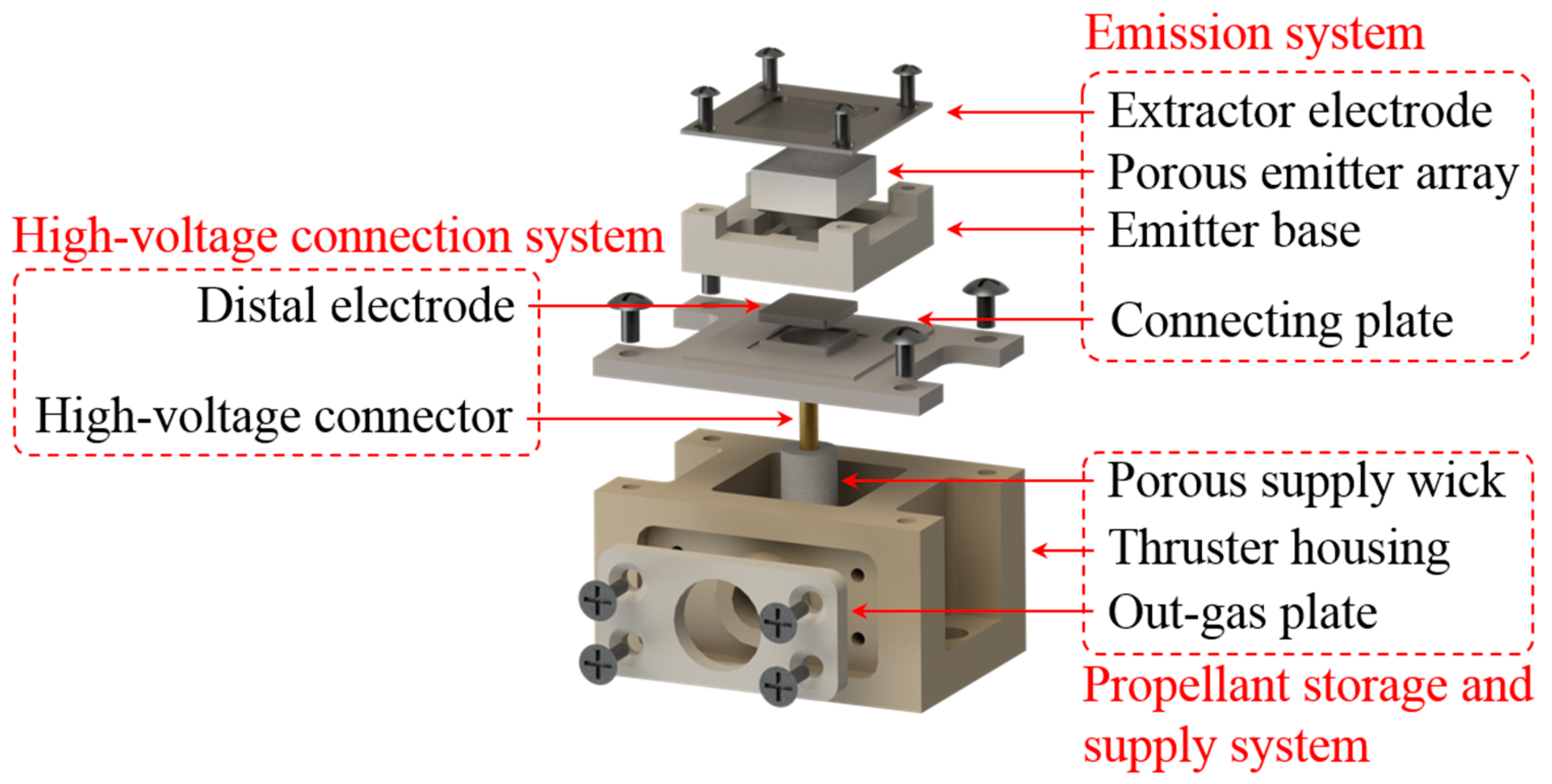
2.1. Thruster Design

An exploded view showing all of the components of the ILET is shown in Figure 1. The thruster design adopts modular thinking; it has three main sub-systems: an emission system, high-voltage (HV) connection system, and propellant storage and supply system. The thruster can be mounted on a PCB circuit board through the hole at its rear. Electric power is applied through the HV connector. As the ILET lifetime is mainly determined by the emission system [13], this thruster can expand its thrust range and total impulse by increasing the thruster modular number and the thruster housing volume to meet different thrust requirements. The failures of the ILET are mainly concentrated on the emission system, and the lifetime of the propellant storage and supply system can be increased by replacing the emission system.
The emission system is composed of an emitter, extractor, emitter frame, and connecting plate. The emitter array contains 361 (19 × 19) discrete emitters, which are approximately 200 μm tall with a radius of 15 μm and a flat tip; they are separated by a pitch of 450 μm. Each emitter has an associated aperture within the extractor. The extractor is a “basin” design made from stainless steel. The thickness of the middle region and the peripheral frame of the basin are 0.1 and 0.5 mm, respectively. The diameter of the grid aperture is 0.3 mm, and the pitch is same as the emitter array.
The HV connection system consists of a porous nickel distal electrode and an HV connector. Because the emitter is dielectric, voltage is applied to the propellant by contacting it through the distal electrode. This voltage application method transfers the area where the electrochemical reaction occurs from the emitter tip to the distal electrode [11], and the contact area between the electrode and the propellant can increase. Therefore, the contact area can eliminate the serious impacts of electrochemical corrosion on the lifetime of the thruster through low-frequency voltage polarity switching [14].
In order to simplify the ILET system, a passive supply propellant tank was used in the prototype [1]. Exhaust holes were arranged on the side of the storage, and hydrophobic PTFE film was used to prevent propellant from leaking during the exhaust process in a vacuum. The polyester fiber wrapping the HV connector acted as a wick to transport propellant from storage to the emitter. The glass fiber filter paper was placed between the distal electrode and the emitter array to improve the stability and uniformity of the propellant supply.

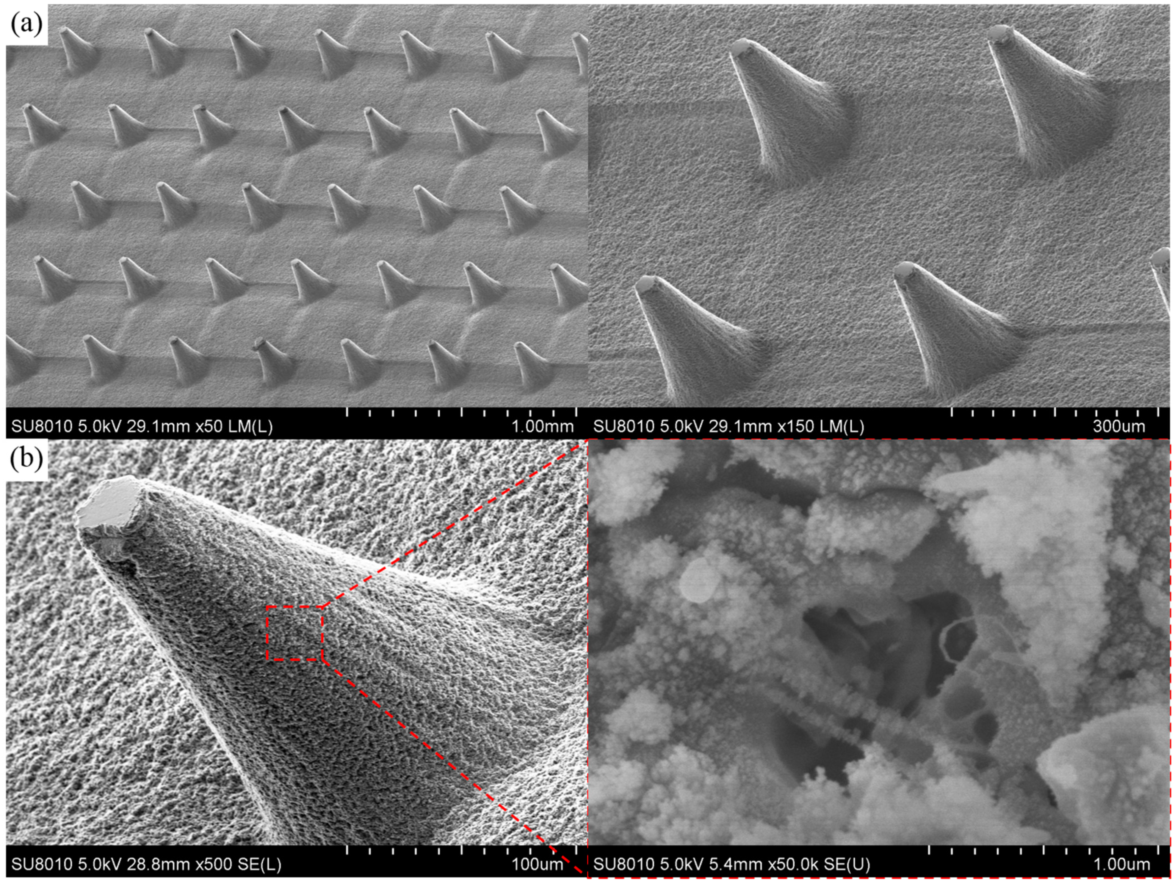
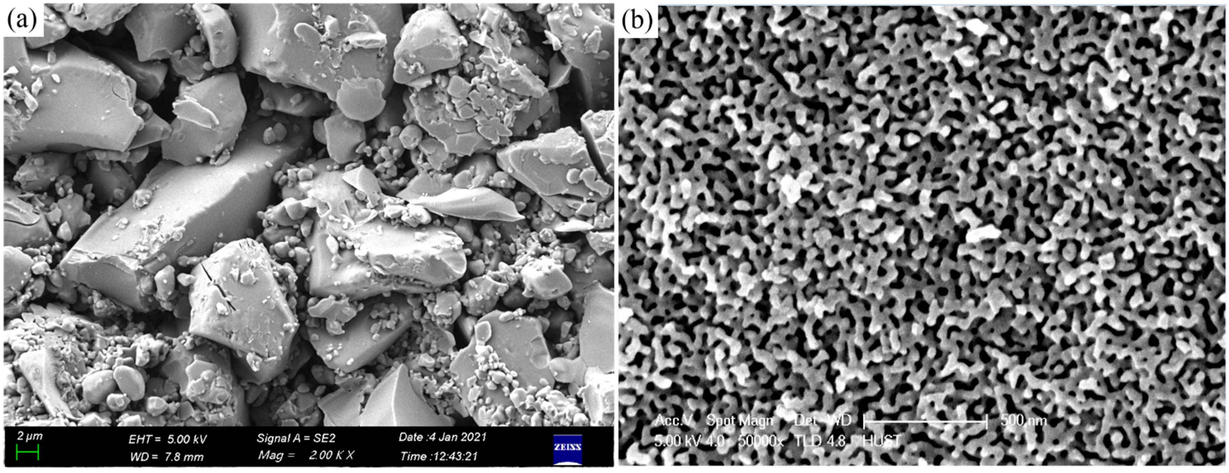
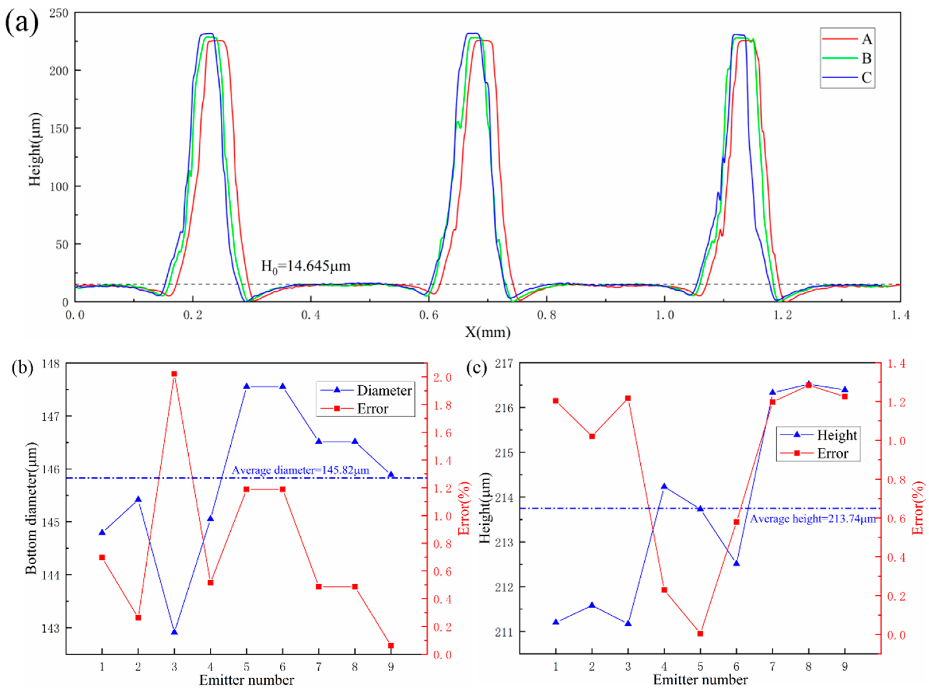
2.2. Emitter Substrate and Fabrication

The performance of an ILET is largely governed by the quality of its emitter features, which is ultimately tied to the manufacturing process. This encompasses both the selection of the substrate material and patterning strategies. Previous iterations of ILETs have focused on profuse sintered borosilicate glass. As shown in Table 1, the sintered borosilicate glass can be divided into seven grades, according to pore size. Because the pore size and uniformity of the emitter can have a direct impact on the performance of the thruster, a smaller pore size is beneficial to obtain a higher specific impulse. As a result, Por.5 grade sintered borosilicate is usually used to manufacture the emitter. An image of the sintered borosilicate glass is shown in Figure 2a; it can be seen that the size of the powder particles ranges from tens of nanometers to tens of microns. If a large-sized particle spall occurs at the emitter tip during processing, it will have a serious negative impact on the processing accuracy.
To address the natural problems of sintered borosilicate glass, this paper adopts a novel borosilicate glass produced using a phase separation method as the emitter substrate. The pore size and porosity were controlled by the composition ratio of the original material and the phase separation heat treatment conditions. An SEM image of the novel porous glass is shown in Figure 2b. Its pore size is about 25 nm, and its porosity is about 52%. The novel porous borosilicate glass was integrally formed instead of using powder particle sintering, which has a better processability and can effectively avoid the particle spalling problem during the processing of sintered borosilicate.
The characteristic size of the emitter tip is usually on the order of microns; as the traditional machining method has cutting stress and vibration, it is difficult to ensure emitter tip machining accuracy. Because of material compatibility and mask accuracy problems, an emitter array with ideal processing accuracy cannot be obtained using wet processing technology.
The nature of the atomic structure of borosilicate glass makes it suitable for laser processing [2]. In terms of processing principles, laser processing can be divided into two categories: photothermal and photochemical processing. From the processing point of view, photochemical processing is very attractive because it can produce an ultra-fine feature resolution on any material, simply by exercising appropriate laser parameters. When the laser processing work is done in the photochemical regime, the high-energy photons directly destroy the material’s chemical bonds, and the resulting molecular fragments diffuse and form plasma that take away excess energy in the material and has almost no effect on the material near the processing area. However, for some materials, extremely high radiation intensities are often required to achieve this state. In general, photochemical processes are induced when the time width of a laser pulse is much smaller than the characteristic thermalization time of the ablating medium. Ultrashort pulse lasers are therefore essential for the processing of new porous borosilicate glasses.
In this study, a picosecond laser processing platform, shown in Figure 3, was adopted. The diameter of the Gaussian beam emitted by the picosecond laser (Edgewave) was about 3 mm, which was expanded to 12 mm through an expander (4×), and then entered a laser scanning galvanometer (Scanlab Excelliscan, Puigheim, Germany) and F-theta scanning lens (Linos, Feldkirchen, Germany) through several reflectors to focus on the sample surface for etching.
The picosecond laser had three wavelengths of 1064, 532, and 355 nm, which can be switched, the pulse width was 10 ps, and the repetition frequency was 1–50 MHz. The 355-nm ultraviolet laser was applied to ensure laser processing work in the photochemical regime. The F-theta scanning lens used in this system had an effective focal length of 70 mm and the final focused laser spot diameter was about 5 μm.
The emitter array was processed using the layer-by-layer etching method shown in Figure 4. The cylinder array was etched on each processing layer using the laser scanning path, as shown in Figure 4, and the cylinder’s diameter in each layer increased layer by layer. The required emitter configuration could be fabricated by adjusting the parameters, such as the cylinder diameter, etching depth, and processing layers of each etching layer. In this paper, the emitter was divided into ten layers for processing, the single layer etching depth was 20 μm, the repetition rate of the laser was 2 MHz, and the single pulse energy was 2.5–10 μJ. The laser scanning speed was 3 m/s and the two adjacent spot rates were 80%.
A second low-power scan was used to polish the sharp edges produced by layered etching to prevent the sharpness from the production of the local strong electric field and the non-ideal charged particle emission points from affecting the performance and lifetime of the thruster. The scanning path was consistent with the first layering process during the processing of sharp edges, but the laser power was reduced.
After the emitter was manufactured, the surface morphology of the emitter array was measured by a confocal microscope (NanoFocus MarSurf CM mobile). In order to test the consistency of the emitters, nine emitters (3 × 3) located in the central area of the emitter array were selected as test samples. Three sections, A, B, and C, were set at the position shown in Figure 5 to extract the geometric contours of these emitters.
Figure 6a shows the profile curves of the cross sections of A, B, and C, in Figure 5, where the black dashed line is the average height of the emitter base with a value of H0 = 14.645 µm. The height and bottom diameter of the test samples were used to check the consistency of the emitter array. As shown in Figure 6b,c, the results showed that the deviations in the emitter height and base diameter were below 2%.
Figure 7a shows a SEM image of the emitter array, which shows that there is no obvious melting phenomenon on the surface, and that there is a good consistency between the emitters. Figure 7b shows an SEM image of the surface of a single emitter, and it is found that there is a floc substance on the surface of the emitter, which is mainly produced by plasma deposition, stimulated by the processing. However, the experimental results showed that the emitter can work correctly and the performance was not significantly affected. In addition, laser processing of the surface of the emitter pore characteristics still had a slight impact. The interaction between the material and the laser, as well as the interaction with the plasma expansion, can damage the structure of the material, so that the surface pore of the emitter is slightly larger than the original pore of the material, but this has little effect on the pore characteristics inside the material.

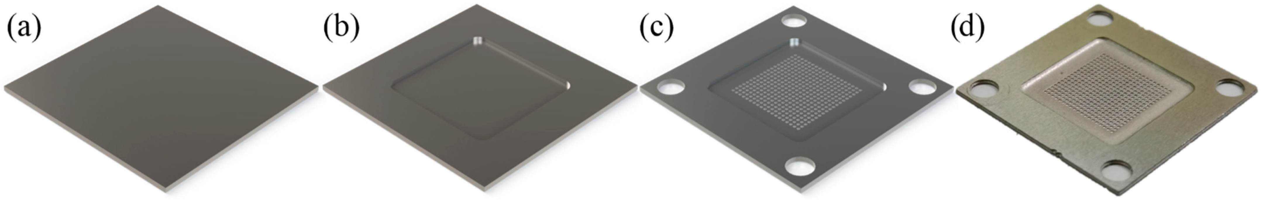
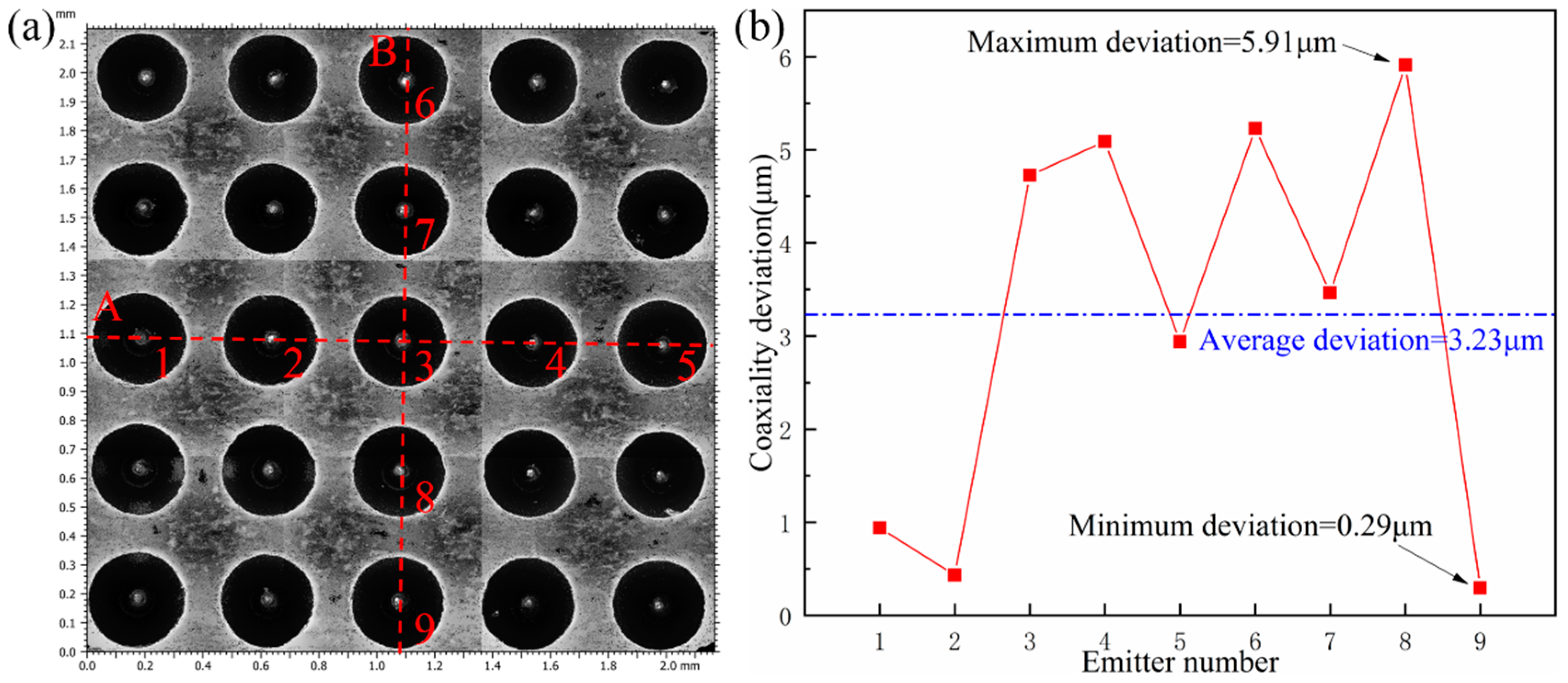
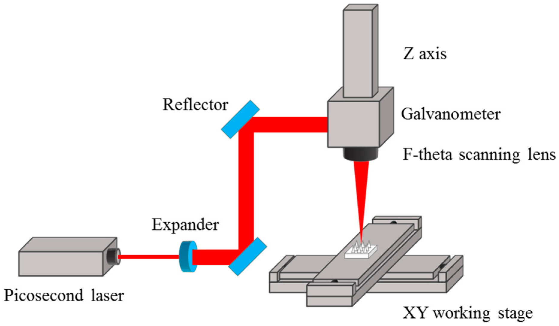
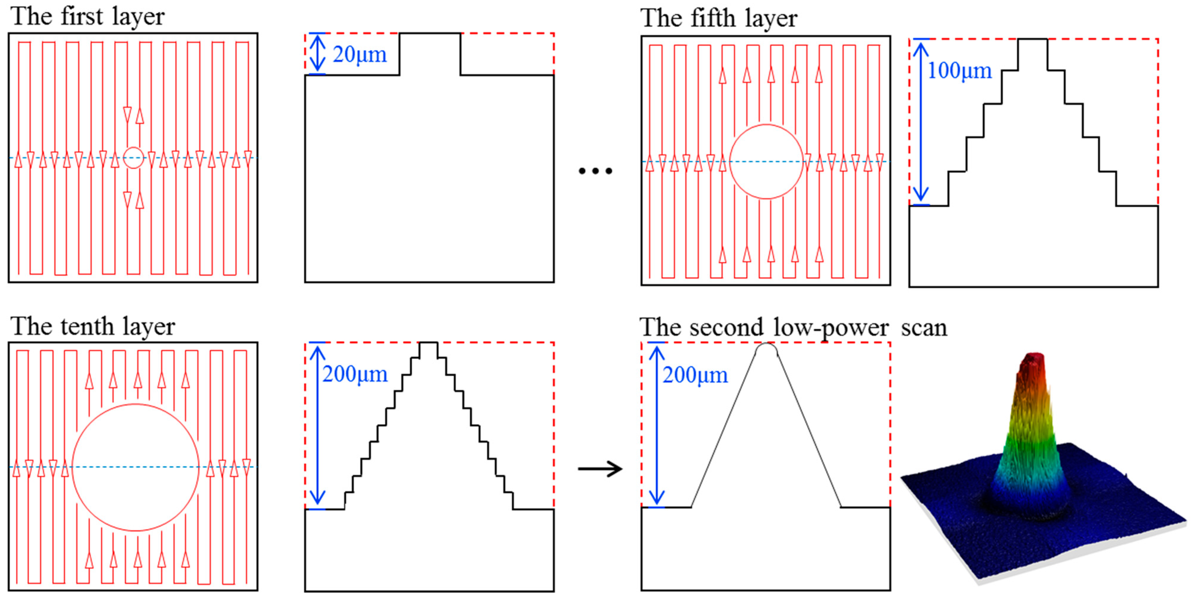
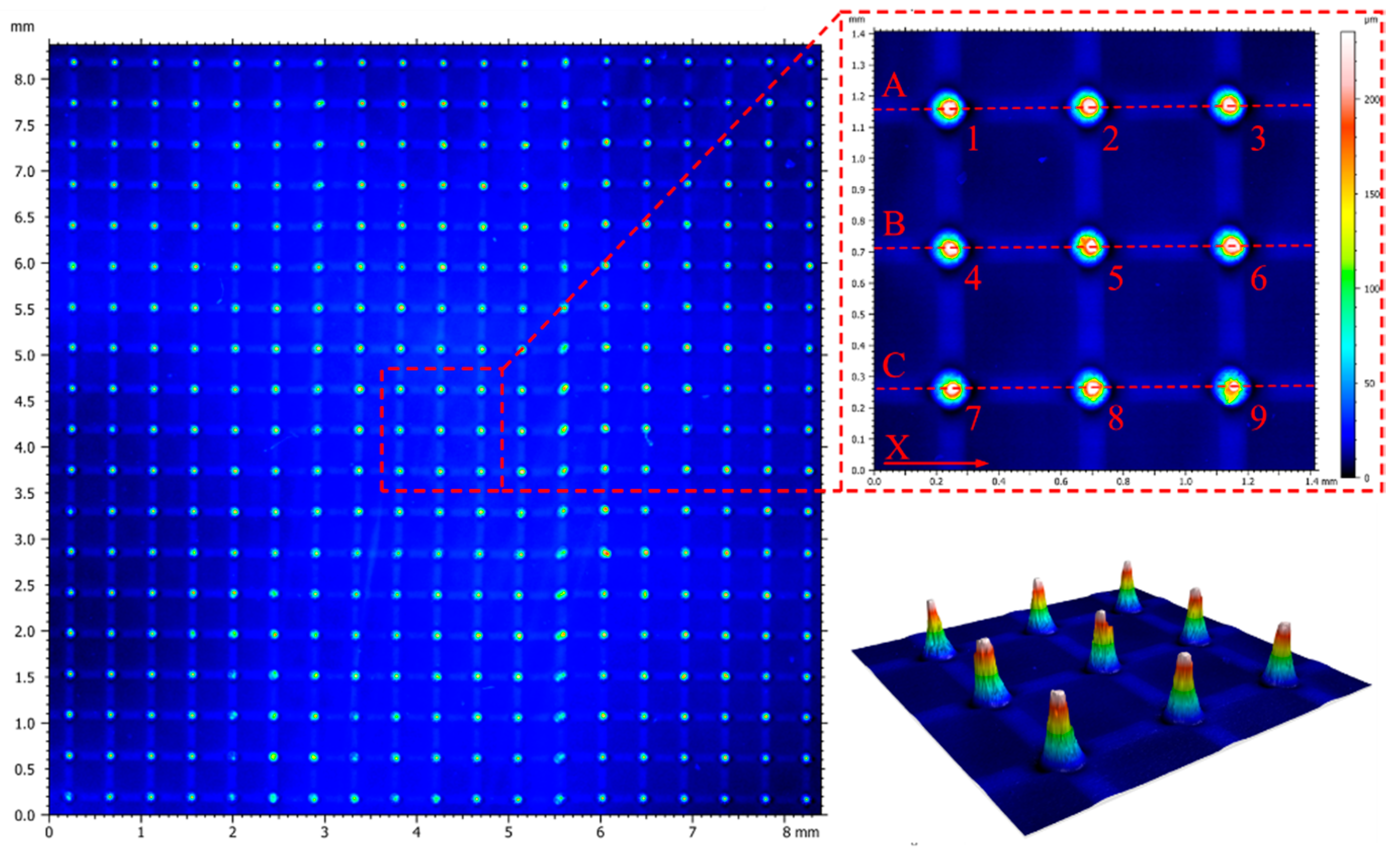
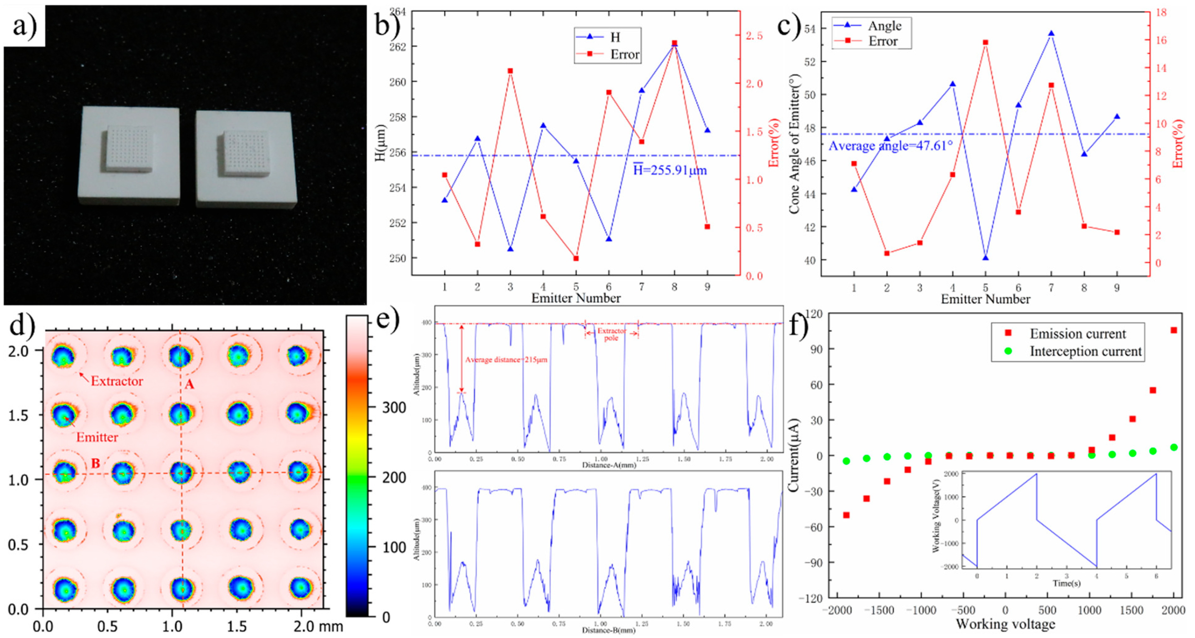
2.3. Unibody Extractor Grid Fabrication

A thin conductive sheet (100 μm) is often used for extractors to reduce the intercepting of accelerating particles. However, due to lack of being sufficient rigid, it is difficult to ensure the tolerances of flatness and aperture localization with traditional processing technology. Consequently, extractor grids are typically manufactured using plasma etching. This technique is not readily available in average machinery plants and is relatively expensive. For this reason, a unibody extractor and the corresponding machining approach was developed.
The unibody extractor used here was designed as a “basin” and manufactured by chemical etching. The manufacturing process is shown schematically in Figure 8. In Figure 8a, a thick stainless-steel sheet (0.5 mm) is used as the substrate. In order to prevent the deflection caused by internal stress, the steel sheet is tempered before processing. During the first process, only the middle area is etched to form a basin, as shown in Figure 8b. The etching depth was about 0.4 mm and was achieved by controlling the etching time according to the steel etching rate. The micro-aperture array was etched on the basin bottom, as shown in Figure 8c. For the design in this paper, an aperture diameter of 300 µm and a pitch of 450 µm was used. The complete unibody extractor is shown in Figure 8d.

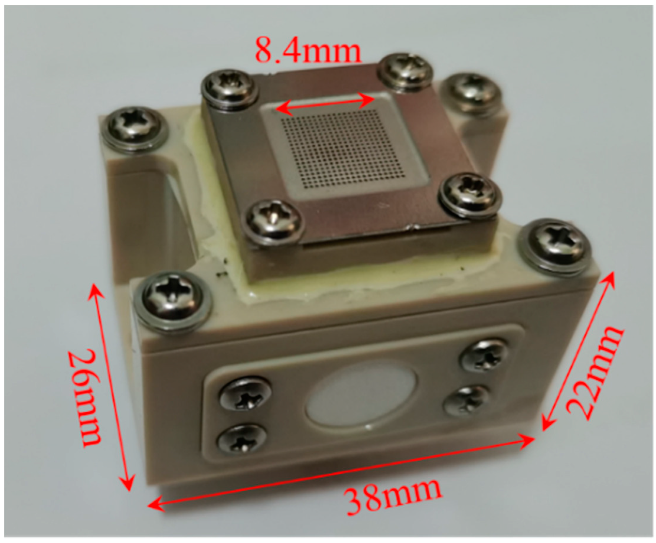
2.4. Thruster Assembly

The emission system is the key module of the thruster, the alignment of the emitters to the extractor apertures is critical for thruster performance. Therefore, the extractor was assembled with the aid of a confocal microscope; the extractor position relative to the emitter is carefully adjusted using a micrometer head. The assembled ILET is shown in Figure 9. The coaxiality deviation between the emitter tip and the extractor pore aperture is an important attribute parameter to measure and evaluate the thruster alignment assembly effect. A 5 × 5 aperture-array located in the middle of the extractor was selected as the measurement zone, and nine extractor apertures, shown in Figure 10a, were set as the measured samples. The measurement result in Figure 10b shows that the average coaxiality deviation was 3.23 μm, the maximum deviation was 5.91 μm, and the minimum deviation was 0.29 μm.

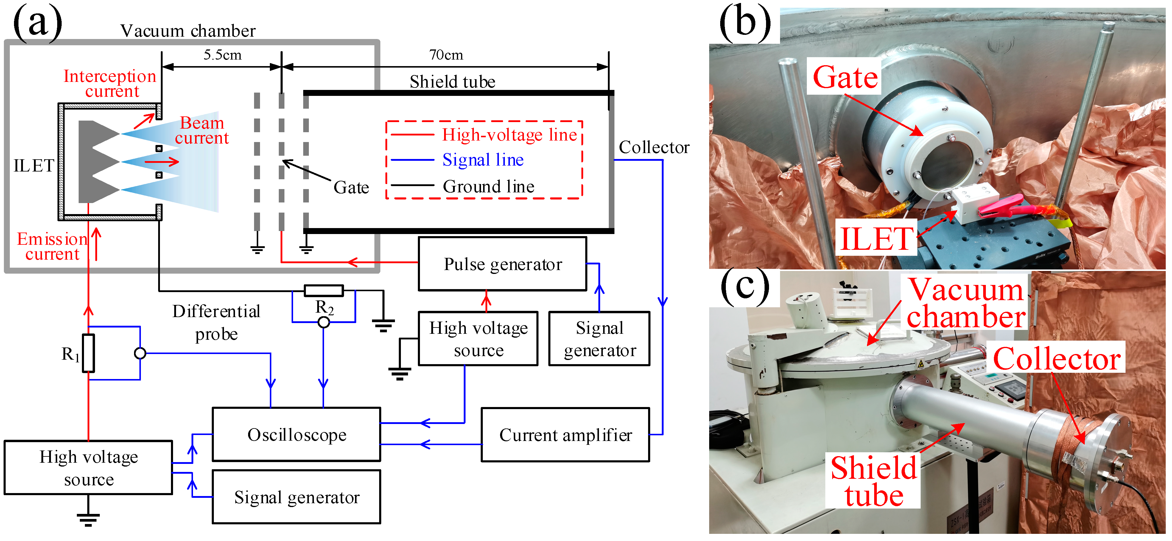
3. Experimental Apparatus and Methods

All experiments presented in this part are performed within a 1 m diameter, 75 cm long vacuum chamber, which includes a cylindrical extender flange and is pumped by a turbopump. All tests are done at pressure lower than 1 × 10⁻² Pa. The experimental setup is outlined schematically in Figure 10. The thruster emitter voltage was controlled using the signal generator (SIGLENT SDG1032X), which was then multiplied by a factor of 1000 using a high voltage amplifier (Matsusada AMT-10B10, ±10 kV). The applied voltage Vem is monitored by recording the amplifier monitor outputs with the Oscilloscope (Tektronix MSO44). The thruster emission current (Iem) and extractor intercepted current (Iem) are measured by monitoring the voltage drop across the two sampling resistors, R1 and R2, using a differential voltage probe. The emission current is generally in the order of 10 μA, and the voltage drop across R1 is 1 V. As a result, the variation on the applied voltage caused by R1 can be ignored.
The time of flight (TOF) spectrometer is developed in house to characterize ion beam compositions. The TOF spectrometer is composed of an electrostatic gate, an ion collector, and a cylindrical shield tube. The electrostatic gate and the collector are respectively mounted on the two ends of the shield tube, which is installed on the extender flange of the vacuum chamber. The electrostatic gate consists of three same circular grids spaced 5 mm apart. The square aperture with side length of 0.3 mm and pitch of 0.35 mm is used in this design. The total transparency of the electrostatic gate is considered to be greater than 51%. The middle grid is pulsed at ±3000 V, which is larger than the ILET working voltage using a pulse generator (DEI PVX-4130) to block the flow of the ions to the collector. When the electrostatic gate is opened, ions will travel to the collector through the field-free region (70 cm in length) defined by the grounded shield tube. The ions traverse the region in an amount of time that decided by their charge-to-mass ration and applied potential. The time dependent current collected by the collector is inputted to a trans-impedance amplifier (FEMTO DHPCA-100) and amplified by a gain of 107 V·A−1, and the amplifier output voltage is recorded by the oscilloscope.

4. Experimental Results and Discussion

All data present in this part are obtained with the thruster operated with ionic liquid propellant 1-ethyl-3-methylimidazolium tetrafluoroborate (EMI-BF4). In order to avoid the trapping gas in the propellant and emitter, the test thruster is degassed in high vacuum for at least 24 h before testing.

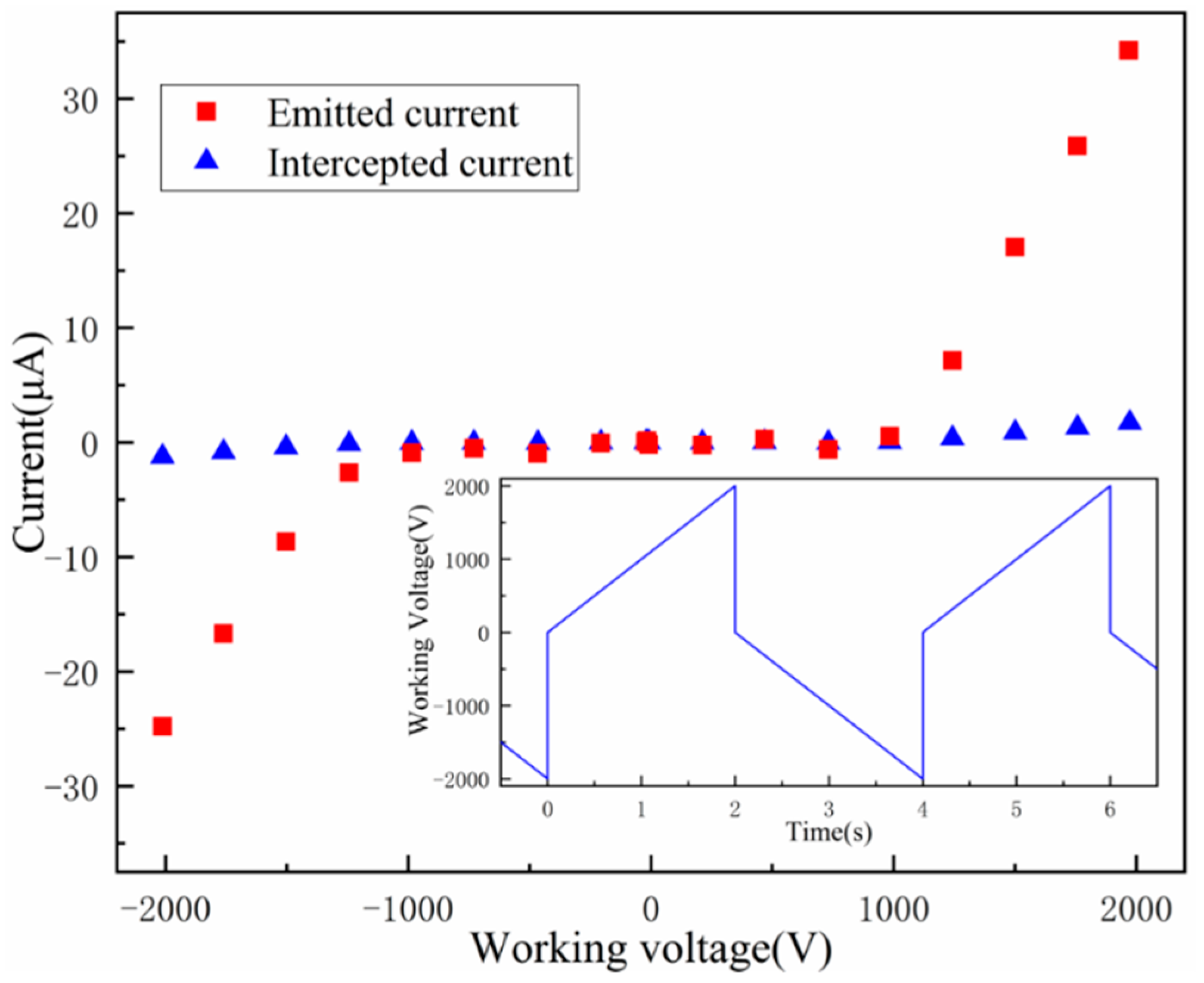
4.1. I–V Characteristics

The measured emission current and the current intercepted by the extractor as a function of operating voltage are shown in Figure 11. The data is the average of three measurements. In order to avoid propellant blood from the emitter tip causing short-circuiting problems, the operating a “slope” like control signal is applied to control the voltage amplifier. This make the thruster fire with the operating voltage peak value at 2 kV and the polar alternating at 0.25 Hz.
As seen in Figure 12, the startup voltage is about ±1000 V for both polarities, which is a little higher than ±800 V, as in a previous study [10]. This is mainly because the separation between extractor and emitter tip is too big, the average distance is about 94 µm in the present ILET, while the emitter tip and the extractor are approximately at the same level in [10]. The data also shows that the emission currents are +34.68 and −25.49 μA at operating voltage of 2 kV for positive and negative emission mode, respectively. It can also be inferred from the Figure that the current intercepted by the extractor is less than 3.5% at operation currents.
Such a small emission current is probably because the pore size of the novel borosilicate is much smaller than that of the sintered borosilicate, resulting in an increased hydraulic impedance and reducing the propellant supply to the emitter tip [9]. After completing the tests described here, the extractor was disassembled from the thruster and examined, the conditions are shown in Figure 13. A few black marks can be found on the emitter array surface (region A and B) and extractor bottom surface (region C and D), which show the evidence of decomposed propellant from firing or intermittent arcing events. Meanwhile, it can be inferred from the extractor residue that there are only about 173 emitters that actually work. This means that the average emission current of per emitter can reach 200.46 nA at the maximum operating voltage.

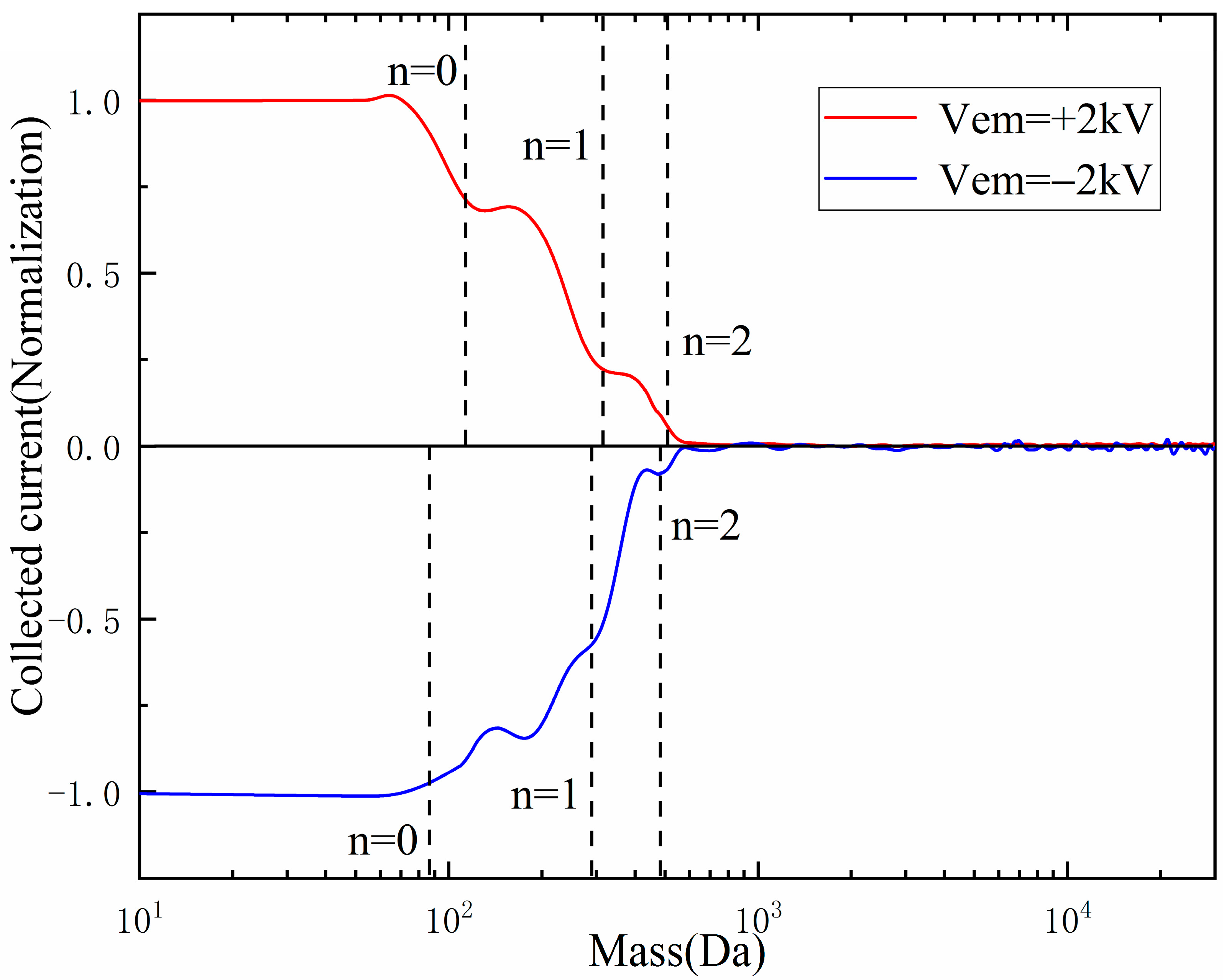
4.2. Mass Spectra of Beam
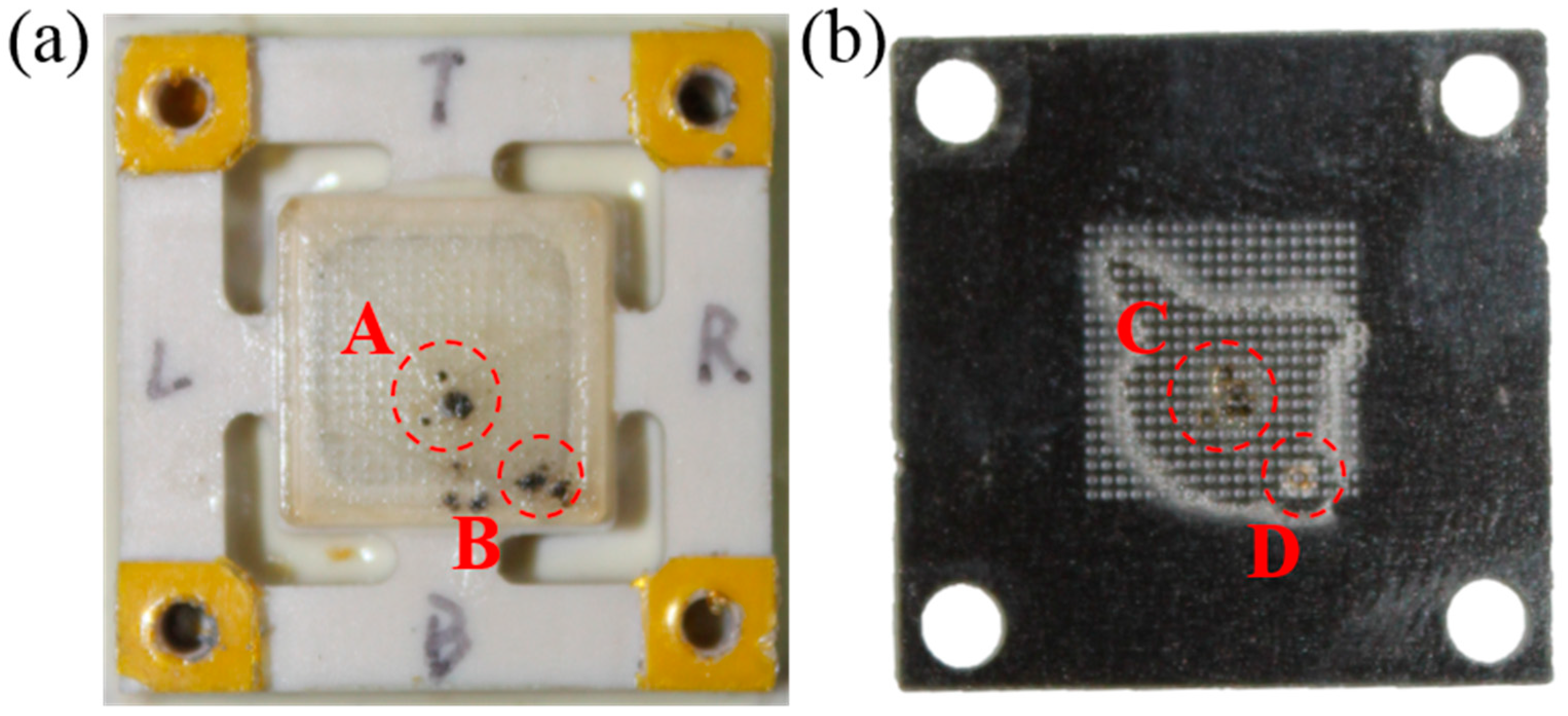
In these experiments, the thruster is positioned on the electrostatic gate central axis at a distance of 5.5 cm. The beam component is obtained in several steps: firstly, the electrostatic gate is triggered by a square pulse several times with the thruster inactive, the signal at the collector is recorded, and the background noise signal fb(t) of the TOF spectrometer is obtained after averaging the measurements data. Secondly, with the thruster operating, the electrostatic gate is triggered by the same pulse and the signal at the collector is recorded to obtain the original signal f0(t) of the TOF spectrometer. Finally, the f0(t) is processed and analyzed to obtain the thruster beam composition.
There are several analysis steps required to extract useful data from the original signal f0(t). Firstly, the background noise signal fb(t) is subtracted from the original signal f0(t) to get the signal f1(t). This removes some of the ringing signal caused by the gate as well as any non-zero offset from the amplifier [15]. At this point, the steps corresponding to unfragmented ions and ion clusters can be identified based on their flight times. Using the relative current fractions, the beam component can be determined. Based on the masses (m) of the ion and ion cluster, the flight time (t) for the charged particles is computed with Equation (1):
m ( t ) = 2 q V e m ( t L ) 2
where q is assumed to be a single elementary charge. The TOF spectrometry results with the thruster operating voltage at ±2 kV are shown in Figure 14.
For EMI-BF4, the emission ions in pure-ion mode take the form of [EMI-BF4]n[EMI+] for positive emission and [EMI-BF4]n[BF4] for negative emission, where n indicates the number of neutrals present. The masses of the ion species operated with EMI-BF4 are labeled by the vertical dotted lines shown in Figure 14. It can be observed that the steps in the measured data locate primarily near the mass values expected for monomers (n = 0), dimers (n = 1), and trimers (n = 2), with a small fraction of the current contributed by the larger ion such as tetramers (n = 3) and charged droplets. The beam fractions of ion species can be inferred from the steps amplitude. The experimental data indicates that the beam in the positive mode is composed of approximately 33% monomers, 47% dimers, and up to 20% trimers. In negative mode, the data indicates approximately 17% monomers, 16% dimers, and up to 57% trimers and tetramers. The thrust and specific impulse of the thruster can be estimated by Equations (2) and (3):
T = 2 V e m I B L 0 t | d I ¯ d t | d t
I s p = L 0 t | d I ¯ d t | d t g 0 t 2 | d I ¯ d t | d t
where IB is the beam current, g is the gravitational acceleration, Ī is the normalized signal of the collector. The thrust is about 3.66 (Vem = 2 kV) and 2.77 μN (Vem = −2 kV), and the specific impulse is 3742 (Vem = 2 kV) and 3173 s (Vem = −2 kV).

4.3. Discussion

Experimentally pure-ion emission has not been achieved in steady state with an approximated impedance value lower than 1.5 × 10¹⁷ kg/(m−4·s−1) per emitter tip [16]. The permeability (κ) of the novel material is 0.02056 μm2, and the emitter is the flat top configuration (top diameter is 20 μm), assuming the tip curvature radius of 10 μm. The flow impedance Ztotal of a single emitter can be calculated by Equations (4)–(7):
Z s u b = μ L κ D 2
Z i n t = μ 2 π κ 1 1 cos ( α ) ( tan ( α ) R c cos ( α ) h )
Z e x t = 32 γ l n ( 1 + tan ( α ) h / R c ) π 2 r s u r 3 tan ( α )
Z t o t a l = ( 1 Z i n t + 1 Z e x t ) 1 + Z s u b
μ is the EMI-BF4 viscosity, L is the thickness of the substrate, D is the distance between the emitters, α is the half angle of the cone, Rc is the radius of curvature of the apex of the tip, h is the height of the emitter tip, γ is the EMI-BF4 surface tension, rsur is the surface feature size of the emitter.
The theoretical flow impedance of a single novel material emitter is calculated to be about 3.73 × 10¹⁷ kg/(m−4·s−1), and from the flow impedance analysis it can be concluded that the emitter is operating in pure-ion mode.
Ref. [17] studies have confirmed that the single emitter’s emission current is related to the average of charge to mass ratio, the viscosity and density of EMI-BF4, and the radius of curvature of the apex of the tip and flow impedance of the emitter.
I t i p ~ 2 ( q / m ) μ ρ R c Z t o t a l
The emission current ratio between different emitters using the same ionic liquid can be expressed as:
I t i p , 1 I t i p , 2 ~ ( q / m ) 1 R c , 2 Z t o t a l , 2 ( q / m ) 2 R c , 1 Z t o t a l , 1
By comparing the measurement results of [17] and this paper, it is found that the average of charge to mass ratio of the two is less different, and the effect on the emission current ratio is much smaller than that of the flow impedance. The Equation (9) can be simplified to:
I t i p , 1 I t i p , 2 ~ R c , 2 Z t o t a l , 2 R c , 1 Z t o t a l , 1
As shown in Figure 15, this paper previously processed the emitter (9 × 9) of sintered borosilicate (Por.5), the emitter’s half cone angle is 24° and a height of 250 μm, and the distance between emitter tip and extractor bottom is about 100 μm. The results of the confocal microscope are shown below.
The flow impedance of the Por.5 emitter is calculated to be about 2.33 × 10¹⁶ kg/(m−4·s−1), and the average emission current of the single emitter is measured at 1270 nA (2 kV). The emission current of the single novel material emitter can be estimated to be about 100 nA according to Equation (10). In addition, assuming that the 173 emitters are always in operation, the average emission current of the emitter is the minimum, and if the emitter ceases to operate during this period, the average emission current is greater than 200.46 nA. The emission current decreases with the increase of flow impedance, the average emission current of the novel material emitter measured in this paper is less than the Por.5 emitter, and the calculation value of the empirical equation is at the same magnitude, so the measurement result can be considered reliable.
The differences in emission current in different polar voltage operating modes in Figure 12 can be explained by Equation (11):
I = n q s v = Q i f i 2 V e m ( q m ) i
fi is the proportion of each component in the beam. Because the electric field strength of the emitter tip is basically the same in different polar voltage operating modes, assuming that the total charged Q generated by a single emitter per unit of time remains the same, the emission current depends only on the charge to mass ratio and operating voltage.
From [9,15,17] and experimental data, it is found that the ratio of monomers in negative voltage mode is significantly lower than that in positive voltage mode under the same operating voltage with EMI-BF4 as propellant. Therefore, the average charge to mass ratio of the beam in negative voltage mode is relatively low, which directly leads to a lower emission current in negative voltage mode.
According to the measurement results of Figure 12, the ratio of emission current in positive and negative voltage mode is about 1.3605. According to Equation (11) and related assumptions, the emission current ratio is approximately 1.2467 under different polarity using the charge to mass ratio data measured in Figure 14. The above analysis can indirectly verify the validity of the TOF measurement result. However, compared with the results in the literature [9,15,17], the beam components in negative voltage mode still show abnormal proportions, but the components measured in positive voltage mode are similar to the results in the literature. It can be thought that the very small pore of the emitter affects the ion emission in negative voltage mode, resulting in an increase in the polymer ratio.

5. Conclusions

This study reports the fabrication methods and performance characterization of a novel porous-media borosilicate electrospray thruster. Outlines of the thruster components are presented and fabrication methods are described in detail for the key components, such as the emitter array and unibody extractor. The novel porous-media borosilicate glass used as the emitter substrate is integrally formed by a phase separation method. In contrast with the particle sintered glass, it displays outstanding pore structure uniformity and is easy to machine by subtractive processes. The fabrication techniques were developed based on picosecond ultraviolet laser processing, which allowed the emitter array to be fabricated on the substrate at densities comparable to those found throughout the literature. The picosecond ultraviolet laser can directly destroy the material chemical bonds and avoid particle spalling. It was shown that there is an opportunity to attain more controllable emitter shapes than previous materials such as sintered borosilicate glass or metals by using novel borosilicate glass and picosecond laser technology.
The ILET operating with EMI-BF4 is characterized for both polarities. I–V characteristics experimental data showed that the startup voltage for emission was approximately ±1 kV. The data also show that the emission currents are +34.68 and −25.49 μA at an operating voltage of 2 kV for positive and negative emission mode, respectively. Additionally, the current intercepted on the extractor grid was shown to be extremely low, averaging 2.58 and 2.14% across the performance range tested for positive and negative emission modes, respectively. TOF spectrometry’s measurements showed that the ILET operated in the pure-ion mode and the beam was primarily composed of monomers and dimers, and there are almost no large-mass ion and charged droplets in the beam. The performance inferred from the TOF data showed that the thrust was 3.66 μN in positive emission mode and 2.77 μN in negative at the maximum operating power of 70 mW, and the corresponding specific impulse was 3742 s and 3173 s, respectively.
Pore structure uniformity and processability make the novel borosilicate glass a promising candidate for electrospray applications. However, this novel borosilicate glass emitter has a relatively low emission current. There are two main reasons, one is that the small pore size increases the hydraulic impedance and reduces the flow rate. On the other hand, the uneven supply of ionic liquid cause only about 173 emitters (total 361) to actually work during thruster operation. Due to the interest in novel borosilicate glass in the field of propulsion, future work will focus on optimum design of emitter array to increase the emitter density and refine the supply system design.

Author Contributions

Writing—original draft, investigation, and Resources, Y.Y.; Methodology and validation, D.G.; Writing—review and editing, X.L.; Visualization, L.D.; Formal analysis and data curation, B.C.; Project administration, M.C. All authors have read and agreed to the published version of the manuscript.

Funding

This research received no external funding.

Institutional Review Board Statement

Not applicable.

Informed Consent Statement

Not applicable.

Data Availability Statement

The data presented in this study are available on request from the corresponding author. The data are not publicly available due to the relevant regulations of the author’s institution.

Acknowledgments

We sincerely thank the entirety of the Beamed Energy and Electromagnetical Propulsion Laboratory at the National University of Defense and Technology for their contribution to this manuscript. We additionally thank Hao Liu of Wuhan National Laboratory for Optoelectronics, Huazhong University of Science and Technology for his assistance in the manufacturing process of the emitter.

Conflicts of Interest

The authors declare no conflict of interest. The funders had no role in the design of the study; in the collection, analyses, or interpretation of data; in the writing of the manuscript, or in the decision to publish the results.

References

  1. Krejci, D.; Lozano, P.C. Micro-Machined Ionic Liquid Electrospray Thrusters for Cubesat Application. In Proceedings of the 35th International Electric Propulsion Conference, Atlanta, GA, USA, 8–12 October 2017. [Google Scholar]
  2. Coffman, C.S.; Lozano, P.C. On the Manufacturing and Emission Characteristics of Dielectric Electrospray Sources. In Proceedings of the 49th AIAA/ASME/SAE/ASEE Joint Propulsion Conference, San Jose, CA, USA, 14–17 July 2013. [Google Scholar]
  3. Lozano, P.C.; Glass, B.; Martinez-Sanchez, M. Performance Characteristics of a Linear Ionic Liquid Electrospray Thruster. In Proceedings of the 29th International Electric Propulsion Conference, Princeton, NJ, USA, 31 October–4 November 2005. [Google Scholar]
  4. Legge, R.S.; Lozano, P.C.; Martínez-Sánchez, M. Fabrication and Characterization of Porous Metal Emitters for Electrospray Thrusters. In Proceedings of the 30th International Electric Propulsion Conference, Florence, Italy, 17–20 September 2007. [Google Scholar]
  5. Courtney, D.G. Ionic Liquid Ion Source Emitter Arrays Fabricated on Bulk Porous Substrates for Spacecraft Propuslion. Ph.D. Thesis, Massachusetts Institute of Technology, Cambridge, MA, USA, 2011. [Google Scholar]
  6. Lenguito, G.; De La Mora, J.F.; Gómez, A. Scaling up the power of an electrospray microthruster. J. Micromech. Microeng. 2014, 24, 55003. [Google Scholar] [CrossRef]
  7. Máximo, D.V.M.; Velásquez-García, L.F. Additively manufactured electrohydrodynamic ionic liquid pure-ion sources for nanosatellite propulsion. Addit. Manuf. 2020, 36, 101719. [Google Scholar] [CrossRef]
  8. Courtney, D.G.; Dandavino, S.; Shea, H. Comparing Direct and Indirect Thrust Measurements from Passively Fed Ionic Electrospray Thrusters. J. Propuls. Power 2016, 32, 392–407. [Google Scholar] [CrossRef] [Green Version]
  9. Courtney, D.G.; Shea, H. Influences of porous reservoir Laplace pressure on emissions from passively fed ionic liquid electrospray sources. Appl. Phys. Lett. 2015, 107, 103504. [Google Scholar] [CrossRef] [Green Version]
  10. Guerra-Garcia, C.; Krejci, D.; Lozano, P. Spatial uniformity of the current emitted by an array of passively fed electrospray porous emitters. J. Phys. D Appl. Phys. 2016, 49, 115503. [Google Scholar] [CrossRef]
  11. Brikner, N.; Lozano, P.C. The role of upstream distal electrodes in mitigating electrochemical degradation of ionic liquid ion sources. Appl. Phys. Lett. 2012, 101, 193504. [Google Scholar] [CrossRef]
  12. Natisin, M.R.; Zamora, H.L.; A McGehee, W.; Arnold, N.I.; Holley, Z.A.; Holmes, M.R.; Eckhardt, D. Fabrication and characterization of a fully conventionally machined, high-performance porous-media electrospray thruster. J. Micromech. Microeng. 2020, 30, 115021. [Google Scholar] [CrossRef]
  13. Thuppul, A.; Wright, P.L.; Collins, A.L.; Ziemer, J.K.; Wirz, R.E. Lifetime Considerations for Electrospray Thrusters. Aerospace 2020, 7, 108. [Google Scholar] [CrossRef]
  14. Lozano, P.; Martínez-Sánchez, M. Ionic liquid ion sources: Suppression of electrochemical reactions using voltage alternation. J. Colloid Interface Sci. 2004, 280, 149–154. [Google Scholar] [CrossRef] [PubMed]
  15. Miller, C.E. Characterization of Ion Cluster Fragmentation in Ionic Liquid Ion Sources. Ph.D. Thesis, Massachusetts Institute of Technology, Cambridge, MA, USA, 2019. [Google Scholar]
  16. Perez-Martinez, C.S. Engineering Ionic Liquid Ion Sources for Ion Beam Applications. Ph.D. Thesis, Massachusetts Institute of Technology, Cambridge, MA, USA, 2016. [Google Scholar]
  17. Kristinsson, B.Ö. On the Design of Electrospray Emitters and Their Microfluidic Behavior. Master’s Thesis, Massachusetts Institute of Technology, Cambrige, MA, USA, 2017. [Google Scholar]
Figure 1. Exploded view of the ILET assembly.
Aerospace 08 00297 g001
Figure 2. (a) Powder-sintered borosilicate glass and (b) phase-separation porous borosilicate glass image.
Aerospace 08 00297 g002
Figure 3. Schematic overview of the picosecond laser processing platform.
Aerospace 08 00297 g003
Figure 4. Schematic outline of the steps performed to fabricate an emitter array.
Aerospace 08 00297 g004
Figure 5. Emitter array surface topography measurement results.
Aerospace 08 00297 g005
Figure 6. (a) Profile drawing, (b) bottom diameter, and (c) height of the test samples.
Aerospace 08 00297 g006
Figure 7. SEM image of (a) emitter array; (b) single emitter and surface feature.
Aerospace 08 00297 g007
Figure 8. Schematic outline of the steps performed to fabricate a unibody extractor, the (a) substrate are processed for (b) the first process, and (c) the schematic outline and the (d) image after the second processing.
Aerospace 08 00297 g008
Figure 9. Image of an ILET, showing the complete thruster.
Aerospace 08 00297 g009
Figure 10. (a) Image of the 5 × 5 aperture array and (b) the measurement results of the deviation between the emitter tip and extractor’s aperture.
Aerospace 08 00297 g010
Figure 11. (a) Schematic diagram of experimental device, and image of the (b) inside and (c) outside of the vacuum chamber.
Aerospace 08 00297 g011
Figure 12. I–V characteristics for single ILET.
Aerospace 08 00297 g012
Figure 13. Images of the ILET’s (a) emitter array and (b) extractor after testing.
Aerospace 08 00297 g013
Figure 14. Measured emitted ion mass distribution (Vem = ±2 kV).
Aerospace 08 00297 g014
Figure 15. (a) The emitter of sintered borosilicate glass (Por.5), the (b) height and (c) the cone angle of emitter for the test samples, (d) thruster assembly effect and (e) the distance between emitter and extractor, (f) the I–V characteristics for Por.5 emitter.
Aerospace 08 00297 g015
Table 1. Borosilicate classification (ISO 4793-80).
DesignationPore Size (μm)Porosity (%)
Por.00250–50030
Por.0160–25033
Por.1100–16034
Por.240–10036
Por.316–4041
Por.410–1642
Por.51–1.648
Publisher’s Note: MDPI stays neutral with regard to jurisdictional claims in published maps and institutional affiliations.

