Abstract
Gallium nitride high electron mobility transistors (GaN HEMTs), characterized by their extremely high switching speeds and superior high-frequency performance, have demonstrated significant advantages, and gained extensive applications in fields such as aerospace and high-power-density power supplies. However, their unique internal architecture renders these devices highly sensitive to circuit parasitic parameters. Conventional circuit design methodologies often induce severe issues such as overshoot and high-frequency oscillations, which significantly constrain the realization of their high-frequency performance. To solve this problem, this paper investigates the nonlinear dynamic behavior of GaN HEMTs during switching transients by establishing an equivalent impedance model. Based on this model, a detailed analysis is implemented to elucidate the mechanism by which RC Snubber circuits influence the system’s resonance frequency and the amplitude at the resonant frequency. Through this analysis, an optimal RC Snubber circuit parameter is derived, enabling effective suppression of high-frequency oscillations during the switching transient of GaN HEMT. Experimental results demonstrate that the proposed design achieves a maximum reduction of 40% in voltage overshoot, shortens the ringing time to one-twentieth of the original value, and suppresses noise by 20 dB in the high-frequency range of 20 MHz to 30 MHz, thereby significantly enhancing the stability and reliability of circuit operation. Additionally, considering the heat dissipation requirements in high power density scenarios, this work optimizes the layout of devices, and heat sinks to maintain operational temperatures within safe limits, further mitigating the impact of parasitic parameters on overall system performance.
1. Introduction
Gallium nitride (GaN), as a wide bandgap semiconductor (WBG) material, possesses outstanding properties such as high electron mobility, high temperature resistance, and high voltage tolerance. Gallium nitride high electron mobility transistor (GaN HEMT), serving as a typical representative of third-generation WBG semiconductor devices, exhibits unique advantages in high-frequency and high-power-density applications such as aerospace, electric vehicles, fast charging, renewable energy, and data centers [1]. Compared with traditional silicon metal-oxide-semiconductor field-effect transistors (Si MOSFETs) of the same voltage rating, GaN HEMTs feature faster switching speeds. However, due to the effect of circuit parasitic parameters, high-speed switching operations may trigger high-frequency oscillation and voltage overshoot, posing threats to device performance and long-term reliability [2,3].
High-frequency oscillations and voltage overshoot limit the performance of GaN HEMT. Parasitic inductance and capacitance in the package induce oscillations at high and , which will accelerate the aging of WBG devices. High voltage overshoot may cause mechanical failure and the dielectric breakdown in WBG devices. High-speed switching operations will generate high-frequency oscillations, which can lead to electromagnetic interference (EMI) issues that can disrupt control and communication systems. High-frequency oscillations may also cause ground potential fluctuations, consequently making it difficult to comply with electromagnetic compatibility (EMC) standards. Additionally, the high switching speed of WBG devices exacerbates the negative effects of parasitic parameters, thereby imposing more stringent requirements on circuit design. Directly applying circuit design methodologies originally developed for Si MOSFETs may induce switching oscillations and voltage overshoot in GaN HEMTs, consequently jeopardizing system stability [4]. GaN HEMTs encounter more challenges than Silicon Carbide Metal-Oxide-Semiconductor Field-Effect Transistors (SiC MOSFETs) [5]. The coupling effects between parasitic parameters and high-speed switching in GaN HEMTs are significantly more pronounced, resulting in failure risks that substantially exceed those observed in SiC MOSFETs. Due to their compact dimensions and high power density characteristics, GaN HEMTs experience exacerbated electromigration and solder joint fatigue issues. Under voltage oscillations and overshoot conditions, these devices undergo accelerated performance degradation and significant lifetime reduction. In high-frequency and high-power application scenarios, GaN HEMTs impose extremely stringent requirements on parasitic parameters. Once the printed circuit board (PCB) trace inductance exceeds 5 nH, it readily induces oscillations [6,7,8,9,10,11]. Unlike SiC MOSFETs, GaN HEMTs lack intrinsic avalanche capability and are susceptible to irreversible breakdown when subjected to voltage overshoot. This inherent characteristic necessitates the incorporation of additional protective circuits to mitigate voltage overshoot in high-frequency and high-power scenarios, resulting in increased system costs and heightened design complexity. In practical applications, fully leveraging the performance advantages of GaN HEMTs requires many targeted measures, including device design, circuit optimization, and system layout to effectively address the challenges posed by voltage oscillations and overshoot [12,13,14].
Several methods are employed to suppress high-frequency oscillations, including advanced packaging technologies, optimized gate drive, RC Snubber, parasitic parameters, and layout optimization techniques. The advantages and disadvantages of these methods are summarized in Table 1. Optimizing the packaging technologies can reduce parasitic inductance in devices, thereby mitigating switching oscillations. Device-level parasitic parameters in GaN HEMTs can be mitigated through near-field scanning, Kelvin connections, and surface-mount packaging [15]. At the module level, reducing bond wire length decreases inductance. Emerging packaging technologies minimize parasitic inductance through decoupling capacitors, dual-side cooling designs, hybrid packaging, and mutual inductance utilization [16,17,18]. In [19], copper pillars are optimized to reduce parasitic inductance, but it introduces the risks related to current imbalance. For application engineers, improving GaN HEMT performance through packaging enhancements poses universal challenges. WBG devices with fast switching speeds can cause severe oscillations, which increase the risk of gate breakdown [20,21,22,23]. For Si MOSFETs, increasing gate resistance is commonly employed to suppress switching oscillations. However, directly applying this approach to GaN HEMTs degrades their switching performance. Reference [24] proposes a driver-level converter design with the dual capabilities of high-speed response and noise immunity, enabling the effective suppression of high-frequency oscillations. In [25], it introduces Active Overdrive Voltage (AOV) control and Triple-Branch Level Shifter (TBLS) techniques to address the reliability issues caused by dv/dt-induced effects during the high-speed switching of GaN HEMTs. Current driver optimizations often require extra active devices, increasing complexity, cost, and losses, and its parameter constraints also hinder the global optimization of losses, cost, and electromagnetic compatibility (EMC). For the above studies, gate drive optimization techniques often require additional active components, which not only increase circuit design complexity and hardware costs, but also introduce additional system losses and EMC issues.

Table 1.
High-frequency oscillation suppression methods in power electronic systems.
Compared to driver optimization or packaging improvements, RC Snubbers require no complex control circuit, merely external resistors and capacitors, enabling easier integration into existing systems and making them suitable for cost-sensitive applications [26]. RC Snubbers with configurable parameters offer layout-specific adaptability, effectively suppressing oscillations, minimizing impact on switching speed, and reducing additional switching losses [27]. In [28], RC, RCD, and clamped RCD Snubbers are compared. The RC Snubber absorbs turn-off charge but increases turn-on current stress. The RCD Snubber enhances the absorption speed using a parallel diode, though it is affected by reverse recovery. The clamped RCD regulates capacitor voltage to the DC bus level, operating exclusively during oscillations without affecting switching characteristics. Its diode reverse recovery can be resolved using fast-recovery diodes. Reference [28] exhibits limited depth in parasitic parameter modeling, merely qualitatively attributing oscillations to parasitic inductance and capacitance based on experimental observations. Furthermore, it only briefly addresses Snubber resistor design in its theoretical section, without an experimental analysis of how resistor parameters affect switching performance. In [29], it establishes a third-order transfer function model incorporating PCB and power device parameters through Laplace transform and determines the optimal Snubber resistor value via phase margin optimization, achieving a significant reduction in voltage overshoot and circuit losses. Nevertheless, the study does not explicitly address how to balance voltage overshoot suppression with a dynamic response speed. Reference [30] developed a high-frequency equivalent model with parasitic parameters based on a double-pulse test circuit, deriving a seventh-order system expression for drain–source voltage. Through an analysis of this seventh-order system, it quantitatively identifies effective RC parameter regions, demonstrating that a damping ratio exceeding 0.4 achieves satisfactory suppression. However, the parameter optimization process for this 7th-order system remains computationally complex and heavily reliant on theoretical expertise. Furthermore, the generalizability of the proposed methodology to higher-order systems requires further validation, as its applicability beyond GaN half-bridge configurations, such as to other topological structures or device types, needs additional investigation.
PCB layout optimization is crucial for suppressing high-frequency oscillations and the voltage overshoot of GaN HEMTs. This method, when combined with an RC Snubber, achieves the enhanced suppression of oscillations and voltage overshoot. PCB parasitic parameters can significantly degrade RC Snubber effectiveness. Therefore, optimizing PCB layout to reduce parasitic inductance and shorten current paths is essential for enhancing Snubber performance. In high-frequency and high-power scenarios, PCB parasitic parameters become even more critical in RC Snubber design. In [2], the impacts of common-source inductance and power loop inductance are analyzed, with comparisons between horizontal and vertical layouts. Simultaneously, an optimized single-layer design is proposed to reduce parasitic inductance and voltage overshoot. Nevertheless, it neglects the nonlinear capacitances of GaN HEMT and the coupling interactions between LC and RC circuits. According to [31], the proposed novel layout achieves parasitic inductance in the power loop comparable to or lower than conventional designs, significantly reducing the peak temperature rise across operating modes. This approach optimizes both electrical and thermal performance by simultaneously minimizing power loop parasitic inductance and thermal impedance. Nevertheless, it does not quantify specific parasitic parameter values or their impact on switching losses through precise methods such as finite element analysis. Reference [32] analyzes three power loop structures and implements minimal current return paths through multilayer PCB design, thereby reducing parasitic inductance. Meanwhile, the study derives magnetic field and flux distributions based on the Biot–Savart law to propose an analytical method for calculating stray inductance. These methods have limited practical applicability and may suffer from potential errors due to packaging the data provided by manufacturers. Previous studies have not adequately considered the mutual effects between RC Snubber design and PCB layout optimization.
To solve the above problems, this paper investigates the coupling effects between RC Snubber design and PCB layout optimization to address the practical challenges in GaN-based half-bridge circuits. Experimental results demonstrate that the designed circuit effectively suppresses high-frequency oscillations, significantly reduces overshoot voltage, shortens the ringing time, and attenuates noise at high frequencies during the switching transients of GaN HEMTs. Compared to existing studies, the main contributions of this paper are summarized as follows:
- An equivalent impedance model is constructed for GaN HEMT-based half-bridge circuits during switching oscillations, incorporating parasitic parameters from packaging, PCB, and switching devices. The switching oscillations are decoupled into current and voltage oscillation subsystems, with transfer functions and key parameters derived to characterize oscillatory behavior. Based on this model, the mechanism of RC Snubbers is elucidated, and the influence of RC parameters on the circuit are quantified through simulation and experiments. A multi-level optimization strategy is proposed: calculating initial capacitance values based on target frequency bands, employing algorithms to balance losses and suppression effectiveness, dynamically adjusting parameters with experimental measurements, and incorporating robustness design. Post-optimization results demonstrate a maximum reduction of 40% in voltage overshoot, an oscillation duration shortened to 1/20 of the original value, and high-frequency noise (above 20 MHz) attenuated by 20 dB, significantly enhancing circuit stability.
- A co-optimization methodology for device and heatsink layout is proposed. Q3D simulations are employed to compute electromagnetic field distributions generated by device arrangements, where parasitic inductance and capacitance coupling paths are disrupted through optimized component sequencing and routing strategies. By holistically addressing thermal management and EMI suppression requirements, this approach ensures thermal stability under high-power-density conditions while effectively reducing the negative impacts of parasitic inductance and capacitance on system performance.
The subsequent sections are structured as follows: Section 2 constructs the equivalent impedance model through theoretical derivation and characteristic analysis; Section 3 deeply analyzes the mechanism of RC Snubber and parameter optimization design; Section 4 focuses on the influence of loop inductance on switching ringing through Q3D simulation; Section 5 systematically evaluates the effects of RC Snubber and loop inductance on circuit performance through experimental verification; Section 6 summarizes the research achievements and outlines prospects.
2. Analysis of Switching Process and Oscillation Mechanism
This section elaborates on the switching process of GaN HEMTs, focusing on analyzing the circuit states during turn-on and turn-off oscillations. The GaN HEMT-based half-bridge circuit, as shown in Figure 1, incorporates parasitic parameters from both the devices and the power loop [33]. The power loop comprises the AC and DC loops. Parasitic parameters consist of drain parasitic inductances (, ), source parasitic inductances (, ), gate–drain capacitances (, ), gate–source capacitances (, ), drain–source capacitances (, ), loop inductance (), and loop resistance (). This circuit configuration is more aligned with the operating conditions found in practical applications.
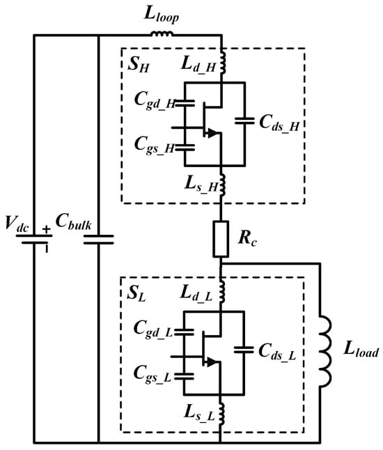
Figure 1.
Schematic of GaN HEMT-based half-bridge circuit.
2.1. Turn-On Process
The turn-on process can be divided into five phases: the turn-on delay phase (), the current rising phase (), the first voltage falling phase (), the second voltage falling phase (), and the turn-on oscillation phase (). The variations in key voltages and currents during each phase are shown in Figure 2. During the turn-on oscillation phase, various parasitic parameters have a significant impact on the circuit, causing intense fluctuations in voltage and current across GaN HEMTs.
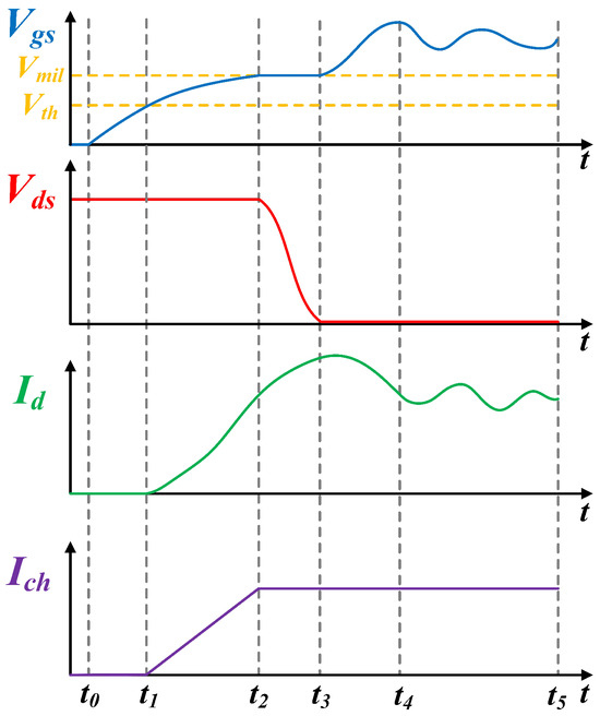
Figure 2.
The switching waveforms of the GaN HEMT during the turn-on process.
During the turn-on oscillation phase, the circuit can be represented by the model shown in Figure 3. The upper switch, acting as the active device, is fully turned on and can be approximated as the resistance (). The oscillation frequency during the turn-on oscillation phase exceeds 10 MHz, at which point the skin effect becomes significant. As a result, the impedance of conductors within the power loop increases at high frequencies, which is the primary cause of the rapid attenuation of oscillation energy during this phase. Then, an equivalent AC resistance () can be introduced into the AC loop, as shown in Figure 3. The lower switch, acting as the passive device, remains off when the upper switch is operating. At this moment, it can be replaced by an LC network, which includes the output capacitance (), , and . During the turn-on oscillation phase, the voltage oscillation on of the GaN HEMT is given by (1).
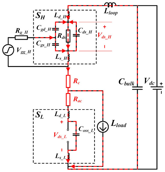
Figure 3.
Equivalent circuit for turn-on oscillation phase.
2.2. Turn-Off Process
The turn-off process is also divided into five phases: the turn-off delay phase (), voltage rising phase (), voltage rising phase (), current falling phase (), and turn-off oscillation phase (). Similarly, the variations in key voltages and currents during each phase are illustrated in Figure 4. During the turn-off oscillation phase, the mutual coupling effects among parasitic parameters (including parasitic capacitance, junction capacitance, and stray inductance) become more pronounced. The dynamic nonlinear characteristics of these parasitic parameters cause a strong frequency modulation effect on the circuit, leading to irregular oscillations in both voltage and current waveforms. Meanwhile, sharp high-frequency spikes are superimposed on the voltage waveform, which oscillates rapidly with high-frequency noise. Both instantaneous voltage and current values experience multiple significant jumps within a very short time, resulting in severe waveform distortion and energy oscillation.
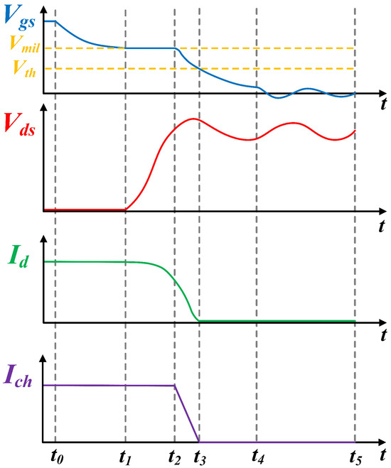
Figure 4.
The switching waveforms of the GaN HEMT during the turn-off process.
For the turn-off oscillation phase, the equivalent circuit is shown in Figure 5. The upper switch, acting as the main control device, is fully turned off. In this case, the upper switch can be replaced by an LC network consisting of the output capacitance , and . Due to the resonant interaction between parasitic inductance and input–output capacitance of GaN HEMTs, distinct oscillation waveforms emerge during the turn-off phase. Similarly to the turn-on oscillation phase, the turn-off oscillation frequency exceeds 10 MHz, requiring to account for the damping effect as well. However, the AC loop during the turn-off oscillation phase exhibits distinct characteristics compared to the turn-on oscillation phase. The position of also differs, as shown in Figure 5. During the turn-off oscillation phase, in addition to the parasitic capacitance and inductance, the reverse conduction path inherent to the lower switch also participates in the power loop. At this stage, the voltage oscillation on is given by (2).
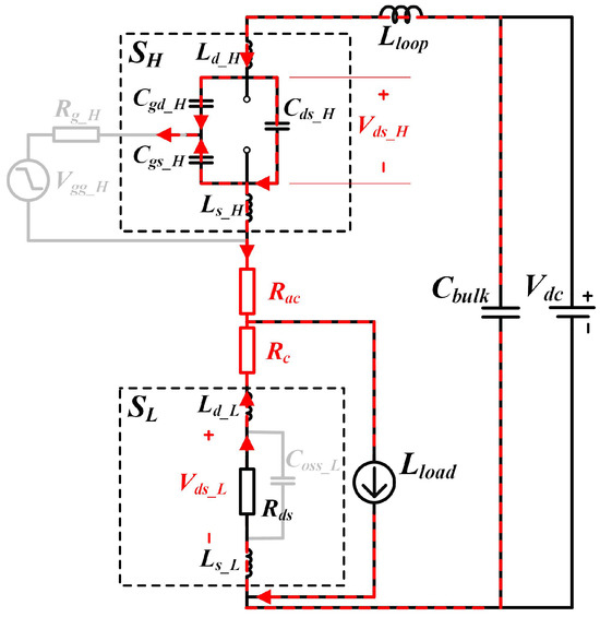
Figure 5.
Equivalent circuit for turn-off oscillation phase.
3. RC Snubber Design
3.1. Analysis of the RC Snubber
The design objective of the Snubber circuit is to mitigate the adverse effects of the switching ringing on various circuit components by reducing the voltage and current rise/fall times during switching operations. The Snubber circuit, consisting of a resistor and a capacitor, strikes an optimal balance between cost and efficiency while aiming for a superior switching ringing suppression performance. The selection of the Snubber capacitor () and Snubber resistor () directly determines the effectiveness of the Snubber in optimizing circuit performance. is selected based on the required amplitude of the voltage spikes to be suppressed and the allowable charging time. A larger results in a more significant suppression effect on voltage spikes. However, it prolongs the charging time, which may degrade the circuit’s response speed. should be chosen by considering both the capacitor charging time and the allowable power loss. A smaller shortens the charging time of but increases the power loss. The RC Snubber in this study is connected in parallel with the drain–source terminals of the power device, as shown in Figure 6. The operating cycle of the Snubber circuit, which directly corresponds to that of the half-bridge circuit, is divided into two phases: the turn-on and turn-off stages.
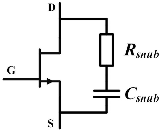
Figure 6.
Schematic of the Snubber circuit.
The working principle during the turn-on stage is illustrated in Figure 7a. When the switching device is turned on, the current begins to flow through it. At this point, the capacitor is discharged through the resistor and the discharging current gradually increases. This capacitor limits the rise rate of the current during the turn-on of the switching device, thereby reducing turn-on losses and EMI. Due to the presence of the capacitor, the voltage rise rate across the switching device is slowed down, effectively mitigating the voltage spike. During the discharging process, the resistor limits the discharging current to prevent excessive current from damaging the switching device or other components.
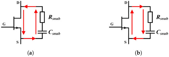
Figure 7.
Schematic of the Snubber working principle. (a) Turn-on; (b) Turn-off.
The working principle of the turn-off stage is illustrated in Figure 7b. When the switching device is turned off, the current flowing to this device rapidly drops to zero. The load inductor () provides freewheeling energy to the half-bridge, generating a reverse voltage spike across the switching device. At this point, begins to charge, absorbing the energy of the circuit to suppress the voltage spike. During the charging process, the resistor dissipates part of the energy, further reducing the voltage spike. It also controls the charging speed of the capacitor to prevent excessive charging current from damaging the circuit components.
3.2. Acquisition of RC Snubber Parameters
The appropriate values of the key parameters and of the Snubber circuit need to be determined from actual circuit experiments. As shown in Figure 8, in the actual circuit, the RC Snubbers are connected in parallel across both the active and passive switches to reduce interference.
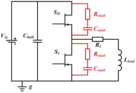
Figure 8.
MPT circuit with RC Snubbers.
This paper establishes an impedance analysis model to determine accurate values for and . Based on the circuit structure shown in Figure 8, this model incorporates various parasitic parameters in the power loop, ultimately producing the equivalent circuit model for the turn-on oscillation stage (Figure 9a) and the turn-off oscillation stage (Figure 10a). During the switching oscillation stage, the upper switching device can be modeled as a series combination of the parasitic inductor ( + ) and the device’s on-resistance (), while the lower switching device can be modeled as and . Since the upper and lower switching devices in the circuit structure of this paper are identical, parameters with the same values are not differentiated. Additionally, the effects of the parameters , , , and must be considered. During the turn-on oscillation stage, high-frequency oscillation occurs in the loop of the lower switching device. In this case, is in series with the lower switching device, and the RC Snubber for the upper switch is shorted and can be neglected. The equivalent circuit at this point is shown in Figure 9b. Since the value of is significantly larger than that of the parasitic capacitance, its influence can be neglected. The final equivalent impedance circuit for the switching device during the turn-on oscillation stage is presented in Figure 9c, where and . During the turn-off oscillation stage, the upper switching device can be modeled as a series combination of and , while the lower switching device can be modeled as a series combination of and . The parameter also needs to be considered. During the turn-off oscillation period, high-frequency oscillation occurs in the loop of the upper switching device. In this case, is in series with the upper switching device, and the RC Snubber for the lower switch is shorted and can be neglected. The equivalent circuit at this point is shown in Figure 10b. The final equivalent impedance circuit for the switching device during the turn-off oscillation stage is presented in Figure 10c, where the values of and are the same as those in the final turn-on model. By combining Figure 9 and Figure 10, it can be observed that both turn-on and turn-off oscillations share the same equivalent impedance model, with their impedance expressions obtained by (3).
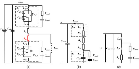
Figure 9.
Equivalent circuits during the turn-on stages of the GaN HEMT: (a) Circuit of Half-bridge with Snubbers; (b) Equivalent circuit of the turn-on stage; (c) Final equivalent circuit of turn-on.
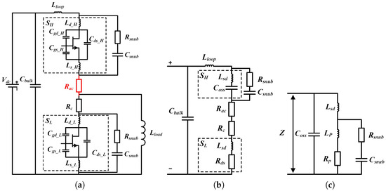
Figure 10.
Equivalent circuits during turn-off stages of the GaN HEMT: (a) Circuit of half-bridge with Snubbers; (b) Equivalent circuit of turn-off stage; (c) Final equivalent circuit of turn-off.
After adding the RC Snubber, the impedance equation corresponding to the switching device is shown in (3). The oscillation behavior of the switching device is directly related to the impedance. The smaller the impedance peak, the more stable the oscillation performance. Based on this characteristic, when selecting the RC parameters, it is necessary to minimize the impedance as much as possible to effectively suppress oscillations.
significantly impacts the resonant characteristics and impedance frequency response of the circuit, as shown in Figure 11. The simulation results indicate that, when is small, the Snubber exhibits weak resonance suppression, resulting in sharp resonance peaks. The system operates close to its natural resonant state with minimal distortion in frequency characteristics. When is larger, the Snubber’s suppression capability is enhanced, leading to flattened peak shapes and improved stability. Significant changes in frequency characteristics occur, affecting the high-frequency response speed of the circuit. As the capacitance increases from 1 nF to 25 nF, the resonant frequency shifts toward lower frequencies and the low-frequency impedance peak decreases continuously. This demonstrates that plays a significant role in suppressing resonance and adjusting frequency. However, the high-frequency impedance peak remains relatively unchanged, which is around 10 . When nF, the low-frequency impedance peak is already lower than the high-frequency impedance peak. Further increasing not only fails to reduce the highest overall impedance peak but also increases additional losses in the RC Snubber. Therefore, selecting nF is sufficient to meet the design requirements for this circuit.
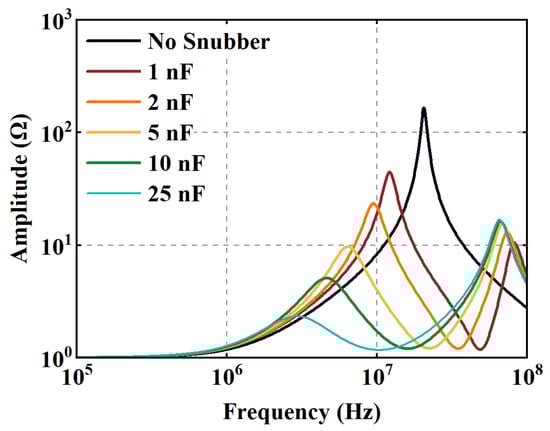
Figure 11.
Frequency-domain response when = 1 , and changes from 1 to 25 nF.
also significantly impacts the circuit impedance. The variation of the resonance characteristic curve is shown in Figure 12. When < 5 , the system is in an underdamped state. As the Snubber resistor value increases, both the high-frequency and low-frequency resonance peaks gradually attenuate. Essentially, the damping resistor suppresses the resonance intensity by dissipating energy as Joule heat, reducing the system’s overstress. As the Snubber resistor value increases, the bandwidth of the resonance peak widens significantly, and its frequency response range expands accordingly. When is around 5 , the system reaches a critically damped state. Meanwhile, the resonance peak becomes flatter, and the frequency coverage range widens further. When > 5 , the system enters an overdamped state, and no low-frequency or high-frequency impedance spikes appear. As increases, the resonant frequency remains the same as without the Snubber, and the impedance peak value rises accordingly.
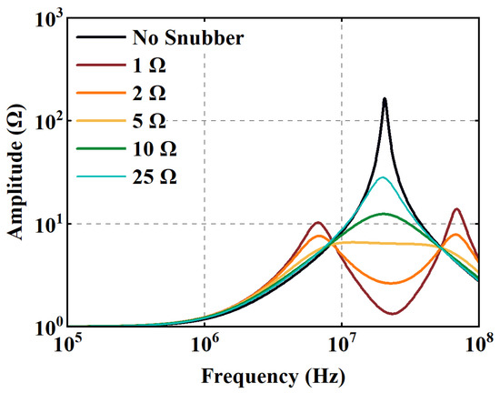
Figure 12.
Frequency-domain response when = 1 nF, and changes from 1 to 25 .
The selection of parameters for and should follow the principle of minimizing the impedance amplitude in order to effectively suppress switching oscillations. Under this premise, efforts should be made to minimize the values of and to reduce losses. The novel RC Snubber design proposed in this paper can significantly reduce the impedance amplitude, which exceeds 100 without the RC Snubber. As shown in Figure 13, when is set to 5 , the high-frequency impedance amplitude is suppressed to below 10 . It can be observed that, as gradually increases, when reaches 5 nF, the low-frequency impedance amplitude is reduced to less than 10 , thus satisfying the principle of minimizing impedance amplitude. Further increasing results in only a limited reduction in low-frequency impedance amplitude, and the overall impedance amplitude does not decrease further. At this moment, the high-frequency impedance amplitude remains unchanged. To avoid an additional losses, the optimal RC parameter combination in this paper is = 5 and = 5 nF, which ensures that the impedance across the entire frequency range remains below 10 .
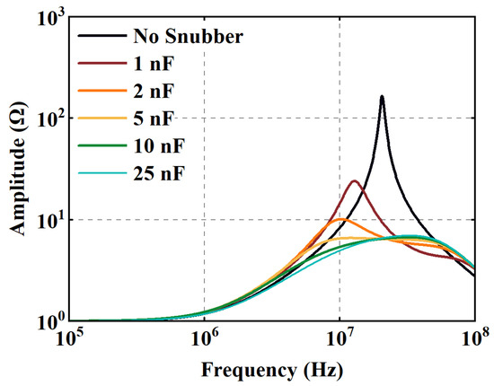
Figure 13.
Frequency-domain response when = 5 , and changes from 1 to 25 nF.
4. Power Loop Inductance Optimization
4.1. Critical Influence Mechanisms of Loop Inductance
In the GaN HEMT-based half-bridge circuit, loop inductance, as a key parasitic parameter, has a decisive impact on the overall system performance. Optimizing loop inductance can enhance the switching performance, reduce electromagnetic interference (EMI), improve system stability, decrease energy loss, and improve load response.
Loop inductance and parasitic capacitance form a resonant circuit during switching transients. Because of a high and , sustained high-frequency oscillations are easily induced in the resonant circuit. These oscillations exhibit a strong correlation with loop inductance. Larger inductance values result in lower resonant frequencies and longer oscillation decay times. Additionally, an increase in parasitic inductance leads to a high voltage overshoot of the switching device.
The high-frequency oscillations can interfere with gate drive signals through coupling paths, causing abnormal fluctuations in the drive voltage. When the fluctuation amplitude approaches the turn-on threshold voltage of the device, the risk of false triggering increases significantly, potentially leading to faults such as bridge arm shoot-through. Moreover, EMI from high-frequency oscillations disrupts surrounding devices, deteriorating the system’s EMC performance. The presence of loop inductance also prolongs the switching times, directly increasing the switching losses. Under high-frequency operating conditions, frequent energy exchange between inductance and capacitance introduces additional reactive power losses, resulting in a significant reduction in system efficiency. Importantly, excessive loop inductance amplifies overshoot, subjecting devices to excessive current stress, accelerating device aging, and shortening their lifetime.
Without loop inductance optimization, the RC Snubber has limitations in improving the switching performance. When loop inductance exceeds a critical value, it not only diminishes the effectiveness of the RC Snubber in suppressing oscillations and mitigating overshoot, but also causes a surge in energy losses within the Snubber circuit, thereby negatively impacting the overall efficiency of the system.
4.2. Layout Optimization Design for Loop Inductance
To mitigate the issues caused by loop inductance, scientific layout design and structural optimization methods are employed to minimize parasitic inductance [2]. During the PCB layout phase, parasitic inductance is reduced by shortening the connection paths between different devices, minimizing the number of pathways, and avoiding narrow traces.
Experimental comparisons show that the layout in Figure 14a exists a high loop inductance due to excessively long grounding paths, large power loop areas and an asymmetric arrangement of the busbar. In contrast, the layout in Figure 14b significantly reduces loop inductance by optimizing the length of grounding wires, reducing the loop area, and achieving a symmetric configuration of the busbar, thus verifying the effectiveness of this layout strategy.
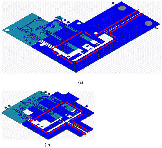
Figure 14.
Power loop with GaN HEMTs. (a) = 57.6 nH; (b) = 45.3 nH.
The calculation equation for is expressed in (4) [7]. The resonant frequency before optimization is = 18.54 MHz. After optimization, it is = 20.84 MHz. It can be derived that reaches 57.6 nH before optimization and is reduced to 45.3 nH after optimization. All the values of parasitic inductances () used in this paper were obtained through Q3D simulation.
A symmetric power loop configuration enables the uniform distribution of current paths, effectively suppressing loop inductance. Furthermore, adopting a multi-layer board vertical layout architecture reduces loop parasitic inductance through the magnetic field cancellation effect. This approach has been validated in relevant literature [2]. GaN power devices exhibit significant heat generation during long-term operation. To mitigate the risk of thermal failure, heat dissipation structures must be integrated on the backside of the devices. Such bottom-side cooling schemes limit the applicability of the vertical architecture design. Therefore, to ensure efficient heat dissipation, a symmetric design of the power loop should be employed to minimize the adverse impact of loop inductance on system performance. Reasonable layout optimization can reduce loop inductance, bringing the RC Snubber closer to its ideal operating state and fully maximizing its damping suppression effect.
5. Experimental Verification
5.1. Test Setup
Among the various experimental methods for parameter acquisition, the Double-Pulse Test (DPT) is commonly used. This method is convenient and reliable, enabling the accurate capture of the circuit’s response during a single transient moment. However, due to its structural limitations, DPT cannot withstand the energy generated by continuous operation, making it incapable of capturing operational parameters during prolonged circuit operation. In practical applications, circuits often need to undergo long-term operation, requiring a shift to alternative testing methods. The Multi-Pulse Test (MPT) simulates the long-term operating state of devices through continuous pulses, allowing the acquisition of operational parameters such as overshoot and oscillation decay under sustained circuit operation. According to [34], MPT can obtain circuit operating parameters that approximate real working conditions, thus meeting the experimental requirements.
The MPT is applied for the analysis of the dynamic characteristics of switching devices, as shown in Figure 15. In this circuit, the upper switch () functions as the active switching device. The lower switch () acts as the passive switching device. , as an inductive load, maintains current continuity during the turn-off phase of switching devices, serving as a freewheeling current source to provide an energy freewheeling path. The load resistor () directly affects the current amplitude and di/dt during switching transients. The value of must be selected within a reasonable range to ensure stable circuit operation.
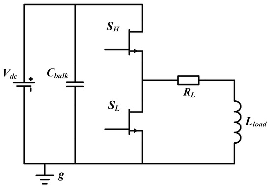
Figure 15.
Schematic of MPT circuit.
Similarly to the DPT circuit, the current path exhibits variations across distinct operating phases. During the turn-on phase, the upper switch () is enabled, while the lower switch () remains off. The current path is depicted in Figure 16a. In this case, the power supply provides energy, and stores energy. During the freewheeling phase, is turned off, and is turned on. Since acts as an inductive load, it maintains current continuity. As shown in Figure 16b, provides the energy to form a freewheeling path. In this phase, releases the stored energy to sustain the load current, preventing abrupt voltage changes, and ensuring the stable operation of the circuit.
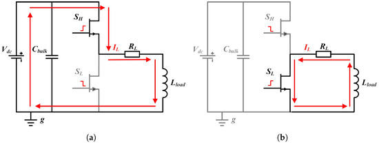
Figure 16.
Schematic of MPT working principles. (a) Turn-on; and (b) Turn-off.
This paper employs the GaN chip from Innoscience (INNO040FQ015A, 40 V/50 A) as the power device in the half-bridge circuit. The driver uses the LM5113 half-bridge driver chip developed by Texas Instruments (TI), which provides two channels of control voltage signals. This chip can respond promptly to high-frequency signals, and its output driving voltage range meets the requirements for turning on and off the GaN HEMT. The control signals are provided by a control module with the TMS320F28335 (150 MHz) from the TI DSP chip as the main controller.
The experimental setup is shown in Figure 17. The PWM signal is generated by a signal generator and used to control the switches. The DC power supply provides energy for the power loop, while the auxiliary power supply is applied for driving GaN HEMTs. Waveforms of , , , and are displayed in real-time via an oscilloscope. Power resistors and air-core inductors form the load circuit simulate the load characteristics during operation. In the PCB design, RC Snubbers must be placed in close proximity to the switching devices to minimize any negative impact of the Snubber circuit on the half-bridge system. The circuit parasitic parameters involved are shown in Table 2.
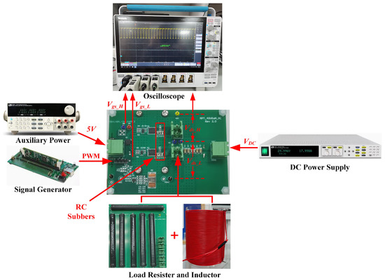
Figure 17.
MPT experimental setup.
Table 2.
Values of the critical parameters in the experimental setup.
5.2. Time-Domain Analysis of Experimental Results
In this paper, the Multi-Pulse Test (MPT) platform is used to conduct experimental analyses on the tested circuit board. The overall experimental diagram for the full cycle of the MPT experiment is shown in Figure 18 and the specific analytical waveforms for switching process analysis are presented in Figure 19, Figure 20, Figure 21, Figure 22, Figure 23, Figure 24 and Figure 25. When the current exceeds 15 A, switching oscillations become extremely severe, which can cause irreversible damage to the GaN HEMT. To ensure that the GaN HEMT operates under normal conditions, the half-bridge circuit must be equipped with the protection of RC Snubbers.
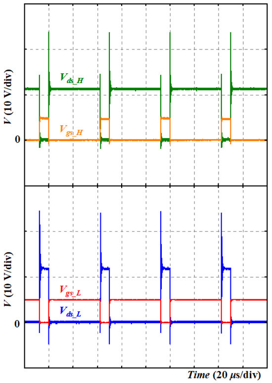
Figure 18.
Overall waveforms of the MPT experiment.
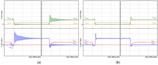
Figure 19.
Switching waveforms ( = 5 A, = 57.6 nH). (a) Without Snubber; (b) With Snubber.
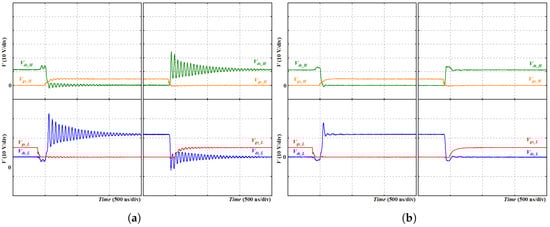
Figure 20.
Switching waveforms ( = 5 A, = 45.3 nH). (a) Without Snubber; (b) With Snubber.
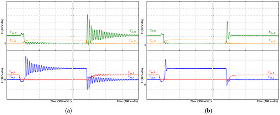
Figure 21.
Switching waveforms ( = 10 A, = 57.6 nH). (a) Without Snubber; (b) With Snubber.
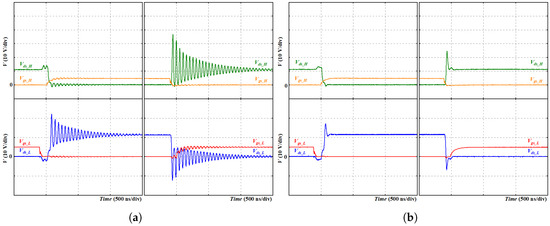
Figure 22.
Switching waveforms ( = 10 A, = 45.3 nH). (a) Without Snubber; (b) With Snubber.
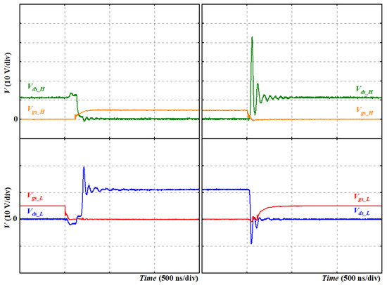
Figure 23.
Switching waveforms with Snubber ( = 15 A, = 57.6 nH).
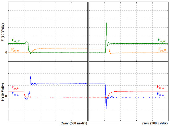
Figure 24.
Switching waveforms with Snubber ( = 15 A, = 45.3 nH).
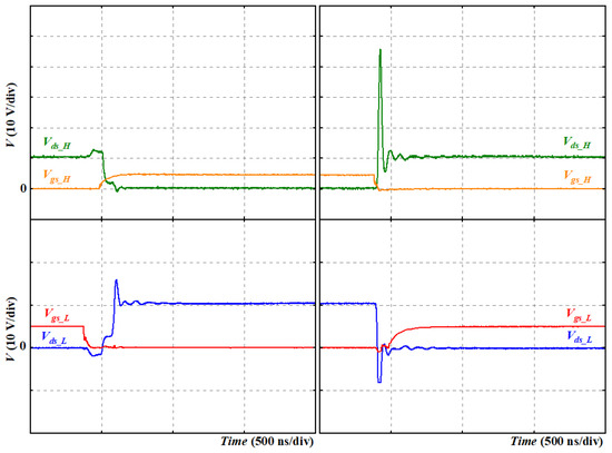
Figure 25.
Switching waveforms with Snubber ( = 20 A, = 45.3 nH).
When only the RC Snubber is incorporated, the maximum voltage of the upper switch () decreases from 25 V to 20 V at a load current () of 5 A, representing a 20% reduction. Under the conditions of = 10 A, drops from 42 V to 31 V, achieving a 26% decrease. Additionally, the RC Snubber shortens the ringing time () to approximately 10% of that in the original circuit. By damping resonance, the RC Snubber significantly suppressed both the voltage spikes and ringing time. However, even with the RC Snubber installed, circuits with a high still exhibited noticeable overshoot, which was more pronounced at = 10 A.
When only is reduced and = 5 A, decreased from 25 V to 24 V, a 4% reduction. When = 10 A, dropped from 42 V to 35 V, achieving a 16% decrease. In this scenario, is reduced from 1.53 to 1.39 , a 9% shortening, indicating that the effect is weaker than that of the RC Snubber. Although the layout optimization can reduce parasitic inductance, its standalone effect is limited, and it needs to be combined with the RC Snubber to achieve better performance.
When the RC Snubber and PCB layout optimization are simultaneously applied, under the conditions of = 5 A, is reduced from 25 V to 14 V, achieving a 44% reduction, while the ringing time of the upper switch () is shortened from 1.4 to 0.13 , a 91% decrease. When = 10 A, is reduced from 42 V to 25 V (40% reduction), and the maximum voltage of the lower switch () is reduced from 24 V to 17 V (29% reduction), both of which are below the maximum voltage of the device (40 V). Under these cases, is shortened from 1.53 to 0.09 , and the ringing time of the lower switch () is reduced from 1.26 to 0.07 , with both achieving a 94% reduction. When = 15 A, reducing from 57.6 nH to 45.3 nH results in the mean of decreasing from 35 V to 25 V, and dropping sharply from 0.12 to 0.08 . Similarly, decreases from 24 V to 21 V, and shortens from 0.11 to 0.07 . When increases to 20 A, with = 45.3 nH and the RC Snubber, rises to 46 V, approaching the tolerance limit of the switch. However, further decreases to 16 V, and the average values of and can be maintained at extremely low levels of 0.07 and 0.06 , respectively. The synergistic scheme of the layout optimization and RC Snubber ensures that the overshoot of the GaN HEMT remains below the voltage withstand threshold, providing a sufficient voltage safety margin. The reduction in parasitic inductance brings the RC Snubber closer to its ideal operating condition.
is significantly affected by the coupling of oscillations. Without any suppression measures, severe noise and fluctuations in lead to extended switching times and the impaired integrity of the drive signal. When = 5 A, obvious oscillations of are observed, posing a risk of false activation, which becomes more intense when = 10 A. When only the RC Snubber is activated are the noise and fluctuations in alleviated. The interference noise of caused by oscillations is reduced, and the risk of false triggering is mitigated. In contrast, PCB layout optimization alone yields limited improvement in disturbance. When employing the PCB layout optimization alone, the effectiveness of noise suppression remains limited. Although shortening parasitic coupling paths can marginally reduce the amplitude of fluctuations, improvements in disturbances are constrained, with oscillations persisting near the threshold level. When the RC Snubber and PCB layout optimization are simultaneously applied, the stability of is significantly enhanced. When = 10 A, fluctuations are within an acceptable range. When = 5 A, stabilizes near zero with notably reduced noise, completely eliminating the hidden danger of false triggering. Detailed experimental data are presented in Table 3.
Table 3.
Parameters of switching waveform in GaN HEMT half-bridge circuit.
5.3. Spectrum Analysis of Experimental Results
By utilizing frequency-domain analysis, the suppression effect of the RC Snubber and layout optimization on oscillations in GaN HEMT can be more intuitively quantified, as illustrated in Figure 26, Figure 27, Figure 28 and Figure 29. The spectrum analysis reveals that the RC Snubber exhibits a significant suppression effect on high-frequency noise, while PCB layout optimization further enhances this effect. Without the RC Snubber, the noise fluctuates drastically in specific frequency bands, with an spike of up to 30 , accompanied by voltage spikes exceeding the system tolerance threshold. After installing the RC Snubber, the amplitude of noise is suppressed by 30 dB. Therefore, the EMC performance of the circuit is substantially improved.
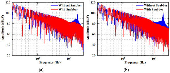
Figure 26.
Spectra of with and without Snubber when = 5 A. (a) = 57.6 nH; (b) = 45.3 nH.
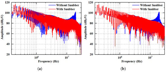
Figure 27.
Spectra of with and without Snubber when = 10 A. (a) = 57.6 nH; (b) = 45.3 nH.
Figure 28.
Spectra of with Snubber when = 15 A. (a) = 57.6 nH; (b) = 45.3 nH.
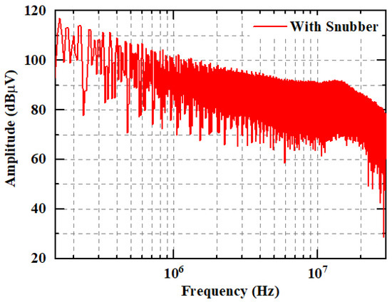
Figure 29.
Spectrum of with Snubber ( = 20 A, = 45.3 nH).
In the frequency band around 20 MHz, when = 5 A, the amplitude of noise is reduced from 99 to 75 , representing a 24.2% decrease, as shown in Figure 26. At a load current of 10 A, the amplitude of noise drops from 101 (without the Snubber) to 75 when the layout optimization and RC Snubber act synergistically, achieving a 25.7% reduction, as illustrated in Figure 27. The main difference between the two scenarios lies in a slight reduction in the noise floor under low load current conditions, while the effectiveness of layout optimization in suppressing high-frequency noise remains stable. This is consistent with the characteristic that high-frequency components are primarily dominated by parasitic parameters. Figure 28 demonstrates that when the load current is 15 A, reducing the loop inductance from 57.6 nH to 45.3 nH decreases the amplitude of noise from approximately 93 to below 90 . Figure 29 shows that, if the loop inductance is fixed at 45.3 nH, an increase in the load current to 20 A causes the overall harmonic amplitude to rise significantly, with the rise being particularly significant in the medium and high-frequency ranges. However, the amplitude of noise can still be controlled around 90 through the optimization of the RC Snubber and loop inductance.
From the perspective of spectral features, without the RC Snubber circuit, the amplitude of noise above 20 MHz reaches 101 , with sharp resonant spikes. These high-frequency components are prone to interfering with surrounding circuits through coupling paths, increasing the risk of circuit failure. In contrast, with the synergistic effect of layout optimization and the RC Snubber, the amplitude of noise at 20 MHz is reduced to 75 and the resonant spikes become flattened, achieving a noise reduction of 25.7%. The mechanism lies in the RC damping effect, which weakens the resonant intensity. Additionally, layout optimization shortens the current paths, mitigating the resonant effects induced by parasitic parameters. The relevant mechanisms can be validated by (3) and (4).
5.4. Influence of and
Figure 30 and Figure 31 illustrate the effects of different and parameter values on switching characteristics. The impedance characteristics revealed in Figure 11 and Figure 12 provide theoretical support for analyzing the experimental phenomena in Figure 30 and Figure 31, collectively establishing a correlation mechanism between RC Snubber parameters and switching characteristics.
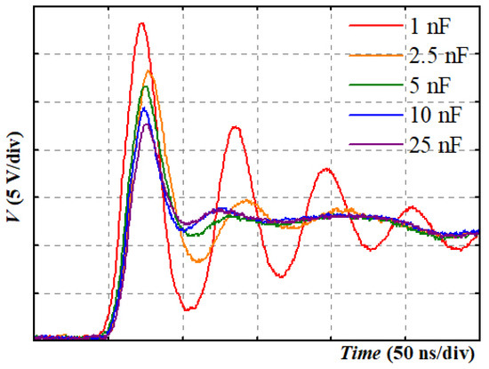
Figure 30.
Experiment waveform of when = 5 , and changes from 1 to 25 nF.
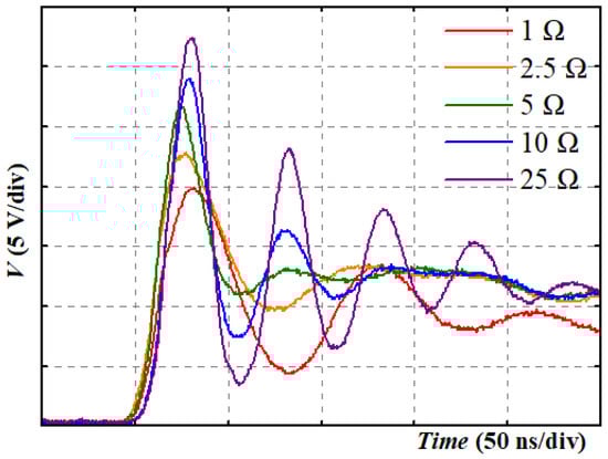
Figure 31.
Experiment waveform of when = 5 nF, and changes from 1 to 25 .
Figure 30 shows that varying values of significantly affect the waveform of . When = 1 nF, the voltage peak reaches the maximum with a large oscillation amplitude. This is due to the limited energy storage capacity of the capacitor with a small value, which results in weak buffering against switching transients. Consequently, it fails to suppress the intrinsic resonance of the LC loop, leading to intense oscillations with slow attenuation and an overshoot of 33.2 V. As increases, the oscillation amplitude of the drain–source voltage gradually decreases, and the convergence time is progressively shortened. When = 5 nF, the oscillation suppression effect meets engineering requirements, with the voltage overshoot reduced to 26.8 V. Meanwhile, the convergence speed significantly improved. This aligns with the optimized impedance characteristics in Figure 30, where the resonant frequency shifts to the low-frequency range and the impedance peak is notably reduced. When = 25 nF, the voltage peak is the lowest, with the smallest oscillation frequency and amplitude. Due to the increased energy storage in the capacitor of the RC Snubber, the mitigation effect on high-frequency oscillations in the drain–source voltage is enhanced, resulting in the effective suppression of the voltage peak. In Figure 11, as the capacitance value of the Snubber capacitor increases, high-frequency oscillations are effectively suppressed. It should be noted that an appropriate capacitance value must be selected to balance power losses and avoid introducing additional parasitic parameters. Additionally, an excessively large may increase the parasitic inductance of and power losses. Thus, a 5 nF capacitor for is determined as the optimal choice, with detailed data presented in Table 4.
Table 4.
Impacts of on voltage oscillation and overshoot.
Figure 31 demonstrates that has a critical influence on the damping characteristics and energy conversion process of the circuit, and its operational mechanism can be systematically explained by combining the impedance characteristic laws revealed in Figure 12. When < 5 , the circuit operates in an underdamped state. As the resistance increases, the oscillation amplitude gradually decreases. This aligns with the characteristic of sharp resonant peaks in Figure 31, where slow oscillation attenuation is attributed to insufficient energy dissipation. When = 5 , the circuit reaches a critically damped state, achieving the optimal oscillation convergence effect. The overshoot is reduced to 26.8 V. This corresponds to the optimal damping matching of impedance characteristics in Figure 31, fully complying with the critical damping design criteria. When > 5 , the circuit enters an overdamped state. As the resistance increases, the output overshoot continues to rise (reaching 32.6 V), with higher voltage spikes, more significant oscillations, and slow attenuation. This is directly associated with the characteristic in Figure 31, where the excessive broadening of the resonant peak leads to the failure of impedance regulation. Experimental results confirm that should not be excessively large. Otherwise, it will not only cause voltage spikes to damage the switching transistor due to excessive overshoot but also weaken the convergence effect of the Snubber circuit. This fully reflects the trade-off mechanism of resistance values between energy dissipation and resonance suppression, with detailed data presented in Table 5.
Table 5.
Impacts of on voltage oscillation and overshoot.
The impedance characteristics depicted in Figure 11 and Figure 12 provide a quantitative explanation for the experimental phenomena observed in Figure 30 and Figure 31. The Snubber capacitor mitigates the overshoot by regulating the resonant frequency and peak impedance, while the Snubber resistor controls the oscillation decay rate by adjusting the damping ratio. The optimal parameter combination derived from experimental optimization ( = 5 , = 5 nF) precisely corresponds to the optimal matching point of impedance characteristics in Figure 11 and Figure 12. At this point, the circuit not only suppresses resonance via the capacitor but also achieves damping balance through the resistor, ultimately resulting in a 40% reduction in voltage overshoot and reducing the number of ringings to 1.
6. Conclusions
This paper focuses on the suppression of switching oscillations in GaN HEMTs using RC Snubbers. Through the theoretical investigation of this paper, the following conclusions are derived:
Through multiple sets of comparative experiments, the synergistic oscillation suppression strategy combining RC Snubbers and loop inductance optimization has been quantitatively validated for its effectiveness in suppressing oscillations for GaN HEMTs. This strategy achieves a balance between high efficiency and reliability. Under = 10 A, the maximum overshoot reaches 42 V without any mitigation measures. Employing only the RC Snubber reduces the overshoot by 26%, while solely optimizing the layout results in a 16% reduction. In contrast, the combination of RC Snubber and layout optimization lowers the overshoot to below 25 V, achieving a 40% reduction, significantly outperforming either strategy individually.
With the synergistic strategy of RC Snubber and layout optimization, the gate drive voltage exhibits no oscillations, completely eliminating the risk of false triggering. The ringing time is reduced below 0.1 (a 95% reduction from the original). In the high-frequency band above 20 MHz, the noise is reduced from 101 to 75 (a 25.7% decrease), significantly improving the electromagnetic environment. Additionally, a high-frequency equivalent model reveals the coupling relationship between , , and , preventing the impedance mismatch between the Snubber circuit and parasitic parameters. The parameter combination of = 5 and = 5 nF achieves critical damping while maintaining lower power losses and a higher oscillation suppression performance.
In summary, the RC Snubber studied in this paper enhances the tolerance of GaN HEMTs under high load conditions, suppresses voltage oscillations and overshoot in the power loop, and prevents high-frequency oscillations from interfering with the drive loop. Meanwhile, loop inductance exacerbates high-frequency oscillations. Optimizing the layout to reduce loop inductance not only suppresses high-frequency oscillations and enhances device tolerance, but also improves the Snubber performance. By combining the RC Snubber and layout optimization, it can achieve the maximum suppression effectiveness of oscillations in GaN HEMTs. This collaborative strategy can significantly improve circuit stability and reliability, offering a quantifiable approach for designing high-power-density power systems.
Future work will focus on adopting novel top-side cooling packaging to investigate the impact of vertical layout on the performance of GaN HEMT-based circuits. By converting the current path from horizontal to vertical, the vertical layout can significantly shorten the physical length of the loop, which is a key principle for optimizing circuit performance. Additionally, combined with a magnetic field cancellation design, the layout can further reduce parasitic inductance. Then, a dual-improvement mechanism with path optimization and parasitic suppression should be established. Ultimately, the above design is expected to significantly reduce the switching oscillation and voltage overshoot, reaching a comprehensive enhancement in the performance of GaN HEMTs.
Author Contributions
Conceptualization, X.L., J.L., and H.L.; Methodology, X.L., H.Z. (Honglang Zhang), and H.L.; Software, C.S. and Y.X.; Validation, X.L. and H.Z. (Hengbin Zhang); Investigation, X.L.; Resources, H.L.; Writing—original draft, X.L.; Writing—review and editing, X.L. and H.L.; Funding acquisition, H.L. All authors have read and agreed to the published version of the manuscript.
Funding
This research was supported by the Major Science and Technology Special Projects in Sichuan Province under Grant No. 2021ZDZX0006.
Data Availability Statement
The original contributions presented in this study are included in the article material. Further inquiries can be directed to the corresponding author.
Acknowledgments
This work was supported by the Aircraft Swarm Intelligent Sensing and Cooperative Control Key Laboratory of Sichuan Province.
Conflicts of Interest
The remaining authors declare that the research was conducted in the absence of any commercial or financial relationships that could be construed as a potential conflict of interest.
References
- Morya, A.K.; Gardner, M.C.; Anvari, B.; Liu, L.; Yepes, A.G.; Doval-Gandoy, J.; Toliyat, H.A. Wide Bandgap Devices in AC Electric Drives: Opportunities and Challenges. IEEE Trans. Transp. Electrif. 2019, 5, 3–20. [Google Scholar] [CrossRef]
- Reusch, D.; Strydom, J. Understanding the effect of PCB layout on circuit performance in a high frequency gallium nitride based point of load converter. In Proceedings of the 2013 Twenty-Eighth Annual IEEE Applied Power Electronics Conference and Exposition (APEC), Long Beach, CA, USA, 17–21 March 2013; pp. 649–655. [Google Scholar]
- Chen, J.; Du, X.; Luo, Q.; Zhang, X.; Sun, P.; Zhou, L. A Review of Switching Oscillations of Wide Bandgap Semiconductor Devices. IEEE Trans. Power Electron. 2020, 35, 13182–13199. [Google Scholar] [CrossRef]
- Kozak, J.P.; Zhang, R.; Porter, M.; Song, Q.; Liu, J.; Wang, B.; Wang, R.; Saito, W.; Zhang, Y. Stability, Reliability, and Robustness of GaN Power Devices: A Review. IEEE Trans. Power Electron. 2023, 38, 8442–8471. [Google Scholar] [CrossRef]
- Buffolo, M.; Favero, D.; Marcuzzi, A.; De Santi, C.; Meneghesso, G.; Zanoni, E.; Meneghini, M. Review and Outlook on GaN and SiC Power Devices: Industrial State-of-the-Art, Applications, and Perspectives. IEEE Trans. Electron Devices 2024, 71, 1344–1355. [Google Scholar] [CrossRef]
- Wu, Y.; Yin, S.; Liu, Z.; Li, H.; See, K.Y. Experimental Investigation on Electromagnetic Interference (EMI) in Motor Drive Using Silicon Carbide (SiC) MOSFET. In Proceedings of the 2020 International Symposium on Electromagnetic Compatibility-EMC EUROPE, Rome, Italy, 23–25 September 2020; pp. 1–6. [Google Scholar]
- Liu, Z.; Li, H. Mitigation of Voltage Oscillation during Turn-off Period of the Silicon Carbide (SiC) MOSFET. In Proceedings of the 2020 IEEE International Conference on Mechatronics and Automation (ICMA), Beijing, China, 2–5 August 2020; pp. 1407–1412. [Google Scholar]
- Wu, Y.; Yin, S.; Li, H.; Ma, W. Impact of RC Snubber on Switching Oscillation Damping of SiC MOSFET With Analytical Model. IEEE J. Emerg. Sel. Top. Power Electron. 2020, 8, 163–178. [Google Scholar] [CrossRef]
- Wu, Y.; Zhang, H.; Yin, S.; Lin, S.; Jiang, T.; Bi, C.; Li, H.; Cheng, Y. Investigation of Conducted Electromagnetic Interference of Three-Level SiC Power Module. In Proceedings of the 2022 Asia-Pacific International Symposium on Electromagnetic Compatibility (APEMC), Beijing, China, 1–4 September 2022; pp. 698–701. [Google Scholar]
- Zaman, H.; Wu, X.; Zheng, X.; Khan, S.; Ali, H. Suppression of Switching Crosstalk and Voltage Oscillations in a SiC MOSFET Based Half-Bridge Converter. Energies 2018, 11, 3111. [Google Scholar] [CrossRef]
- Yang, C.; Pei, Y.; Wang, L.; Yu, L.; Zhang, F.; Ferreira, B. Overvoltage and Oscillation Suppression Circuit With Switching Losses Optimization and Clamping Energy Feedback for SiC MOSFET. IEEE Trans. Power Electron. 2021, 36, 14207–14219. [Google Scholar] [CrossRef]
- Mejia-Ruiz, G.E.; Paternina, M.R.A.; Zamora-Mendez, A.; Rosas-Caro, J.C.; Bolivar-Ortiz, G. A Novel GaN-Based Solid-State Circuit Breaker With Voltage Overshoot Suppression. IEEE Trans. Ind. Electron. 2022, 69, 8949–8960. [Google Scholar] [CrossRef]
- Peng, K.; Eskandari, S.; Santi, E. Characterization and Modeling of a Gallium Nitride Power HEMT. IEEE Trans. Ind. Appl. 2016, 52, 4965–4975. [Google Scholar] [CrossRef]
- Wu, Y.; Yin, S.; Li, H.; Dong, M.; Liu, X.; Cheng, Y. Evaluating Switching Performance of GaN HEMT Using Analytical Modeling. In Proceedings of the 2021 IEEE Workshop on Wide Bandgap Power Devices and Applications in Asia (WiPDA Asia), Wuhan, China, 25–27 August 2021; pp. 434–439. [Google Scholar]
- Ren, Y.; Yang, X.; Zhang, F.; Wang, L.; Wang, K.; Chen, W.; Zeng, X.; Pei, Y. Voltage Suppression in Wire-Bond-Based Multichip Phase-Leg SiC MOSFET Module Using Adjacent Decoupling Concept. IEEE Trans. Ind. Electron. 2017, 64, 8235–8246. [Google Scholar] [CrossRef]
- Zhang, B.; Wang, S. Parasitic Inductance Modeling and Reduction for Wire-Bonded Half-Bridge SiC Multichip Power Modules. IEEE Trans. Power Electron. 2021, 36, 5892–5903. [Google Scholar] [CrossRef]
- Zhang, H.; Wu, Y.; Li, H.; Yin, S.; Jin, S.; Lin, S.; Jiang, T.; Cheng, Y. Design and Evaluation of a 1200-V/200-A SiC Three-Level NPC Power Module. IEEE Trans. Ind. Appl. 2023, 59, 6412–6426. [Google Scholar] [CrossRef]
- Zhang, B.; Wang, S. An Overview of Wide Bandgap Power Semiconductor Device Packaging Techniques for EMI Reduction. In Proceedings of the 2018 IEEE Symposium on Electromagnetic Compatibility, Signal Integrity and Power Integrity (EMC, SI & PI), Long Beach, CA, USA, 30 July–3 August 2018; pp. 297–301. [Google Scholar]
- Song, R.; Zhuo, F.; Wang, F.; Yu, K. Research on Parasitic Inductance Optimization of GaN Paralleled Cascode Power Module. In Proceedings of the 2022 IEEE 13th International Symposium on Power Electronics for Distributed Generation Systems (PEDG), Kiel, Germany, 26–29 June 2022; pp. 1–4. [Google Scholar]
- Sugihara, Y.; Nanamori, K.; Yamamoto, M.; Kanazawa, Y. Parasitic Inductance Design Considerations to Suppress Gate Voltage Oscillation of Fast Switching Power Semiconductor Devices. In Proceedings of the 2018 International Power Electronics Conference (IPEC-Niigata 2018-ECCE Asia), Niigata, Japan, 20–24 May 2018; pp. 2789–2795. [Google Scholar]
- Zhu, J.; Yan, D.; Yu, S.; Sun, W.; Shi, G.; Liu, S.; Zhang, S. 33.2 A 600V GaN Active Gate Driver with Dynamic Feedback Delay Compensation Technique Achieving 22.5% Turn-On Energy Saving. In Proceedings of the 2021 IEEE International Solid-State Circuits Conference (ISSCC), San Francisco, CA, USA, 13–22 February 2021; Volume 64, pp. 462–464. [Google Scholar]
- Li, Q.; Yang, Y.; Wen, Y.; Zhang, G.; Xing, W. Active Gate Driver With the Independent Suppression of Overshoot and Oscillation for SiC MOSFET Modules. IEEE Trans. Ind. Electron. 2025, 72, 2325–2335. [Google Scholar] [CrossRef]
- Lin, X.; Ravi, L.; Mocevic, S.; Dong, D.; Burgos, R. Active Voltage Balancing Embedded Digital Gate Driver for Series-Connected 10 kV SiC MOSFETs. In Proceedings of the 2020 IEEE Applied Power Electronics Conference and Exposition (APEC), New Orleans, LA, USA, 15–19 March 2020; pp. 1611–1616. [Google Scholar]
- Zheng, Y.; Yuan, Q.; Song, D.; Ying, Y.; Zhu, J.; Sun, W.; Zhang, L.; Li, S.; Wang, D.; Zhou, J.; et al. A High-Speed Level Shifter with dVs/dt Noise Immunity Enhancement Structure for 200V Monolithic GaN Power IC. In Proceedings of the 2023 35th International Symposium on Power Semiconductor Devices and ICs (ISPSD), Hong Kong, China, 28 May–1 June 2023; pp. 203–206. [Google Scholar]
- Yu, S.; Zhou, Q.; Shi, G.; Wu, T.; Zhu, J.; Zhang, L.; Sun, W.; Zhang, S.; He, N.; Li, Y. A 400-V Half Bridge Gate Driver for Normally-Off GaN HEMTs With Effective Dv/Dt Control and High Dv/Dt Immunity. IEEE Trans. Ind. Electron. 2023, 70, 741–751. [Google Scholar] [CrossRef]
- Hampe, M.; Stieler, A.; Tieste, K.D. Damping of High-Frequency Oscillations in Power Devices Using Optimized Snubber Circuits. In Proceedings of the 2018 International Symposium on Electromagnetic Compatibility (EMC EUROPE), Amsterdam, The Netherlands, 27–30 August 2018; pp. 1–6. [Google Scholar]
- McMurray, W. Optimum Snubbers for Power Semiconductors. IEEE Trans. Ind. Appl. 1972, IA-8, 593–600. [Google Scholar] [CrossRef]
- Liu, S.; Lin, H.; Wang, T. Comparative Study of Three Different Passive Snubber Circuits for SiC Power MOSFETs. In Proceedings of the 2019 IEEE Applied Power Electronics Conference and Exposition (APEC), Anaheim, CA, USA, 17–21 March 2019; pp. 354–358. [Google Scholar]
- Letellier, A.; Dubois, M.R.; Trovao, J.P.; Maher, H. Overvoltage Reduction with Enhanced Snubber Design for GaN-Based Electric Vehicle Drive. In Proceedings of the 2017 IEEE Vehicle Power and Propulsion Conference (VPPC), Belfort, France, 11–14 December 2017; pp. 1–6. [Google Scholar]
- Chen, J.; Luo, Q.; Wei, Y.; Zhang, X.; Du, X. The Sustained Oscillation Modeling and Its Quantitative Suppression Methodology for GaN Devices. IEEE Trans. Power Electron. 2021, 36, 7927–7941. [Google Scholar] [CrossRef]
- Glaser, J.S.; Helou, A. PCB Layout for Chip-Scale Package GaN Fets Optimizes Both Electrical and Thermal Performance. In Proceedings of the 2022 IEEE Applied Power Electronics Conference and Exposition (APEC), Houston, TX, USA, 20–24 March 2022; pp. 991–998. [Google Scholar]
- Letellier, A.; Dubois, M.R.; Trovão, J.P.F.; Maher, H. Calculation of Printed Circuit Board Power-Loop Stray Inductance in GaN or High di/dt Applications. IEEE Trans. Power Electron. 2019, 34, 612–623. [Google Scholar] [CrossRef]
- Wu, Y.; Yin, S.; Dong, M.; Jin, S.; Li, H.; Cheng, Y.; See, K. Prediction of overshoot and crosstalk of low-voltage GaN HEMT using analytical model. IET Power Electron. 2022, 12, 1295–1321. [Google Scholar] [CrossRef]
- Liu, X.; Li, H.; Wu, Y.; Wang, L.; Yin, S. Dynamic Dead-Time Compensation Method Based on Switching Characteristics of the MOSFET for PMSM Drive System. Electronics 2023, 12, 4855. [Google Scholar] [CrossRef]
Disclaimer/Publisher’s Note: The statements, opinions and data contained in all publications are solely those of the individual author(s) and contributor(s) and not of MDPI and/or the editor(s). MDPI and/or the editor(s) disclaim responsibility for any injury to people or property resulting from any ideas, methods, instructions or products referred to in the content. |
© 2025 by the authors. Licensee MDPI, Basel, Switzerland. This article is an open access article distributed under the terms and conditions of the Creative Commons Attribution (CC BY) license (https://creativecommons.org/licenses/by/4.0/).