
Design and Validation of a Photoelectric Current Measuring Unit for Lunar Daytime Simulation Chamber


Abstract
1. Introduction
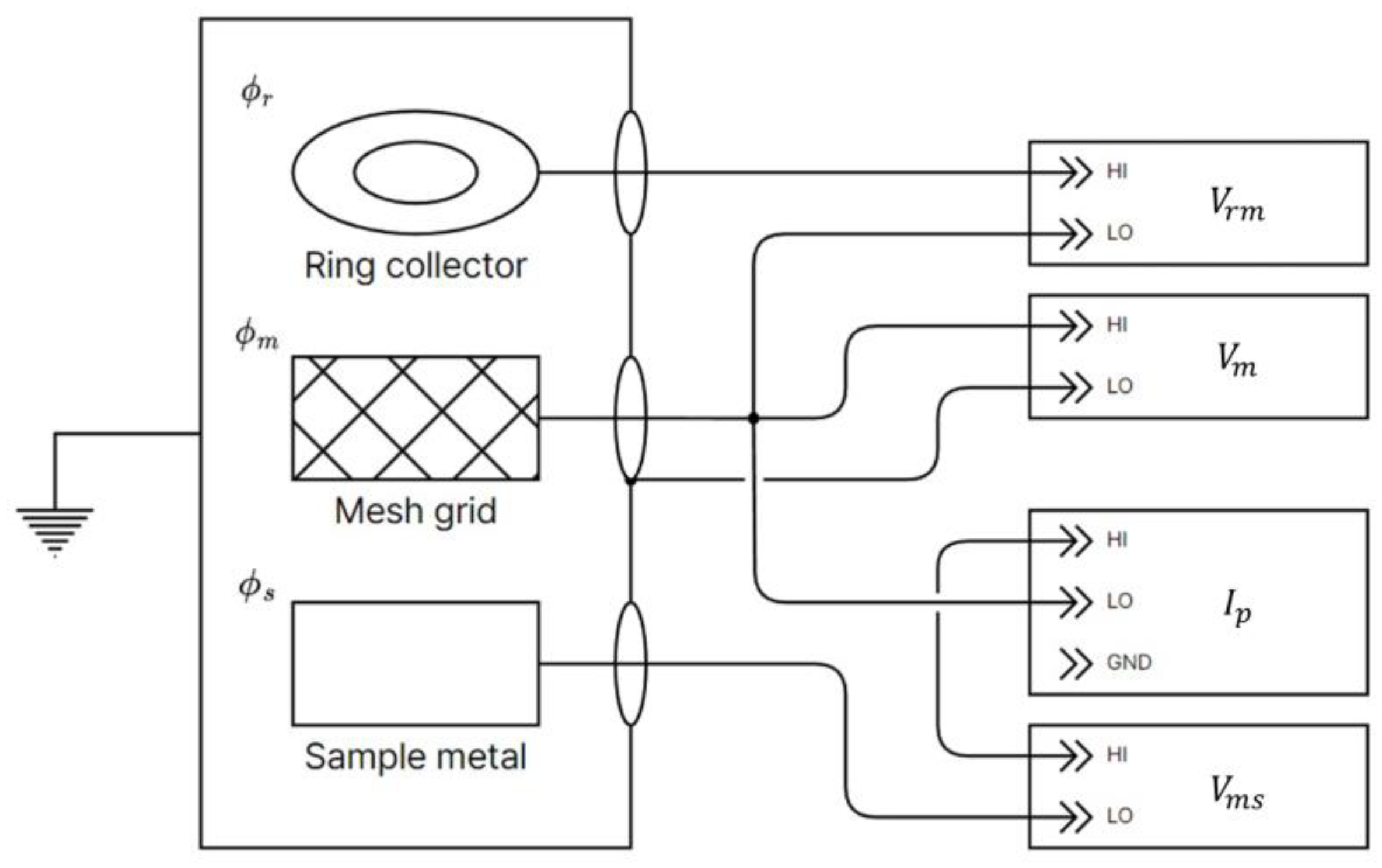
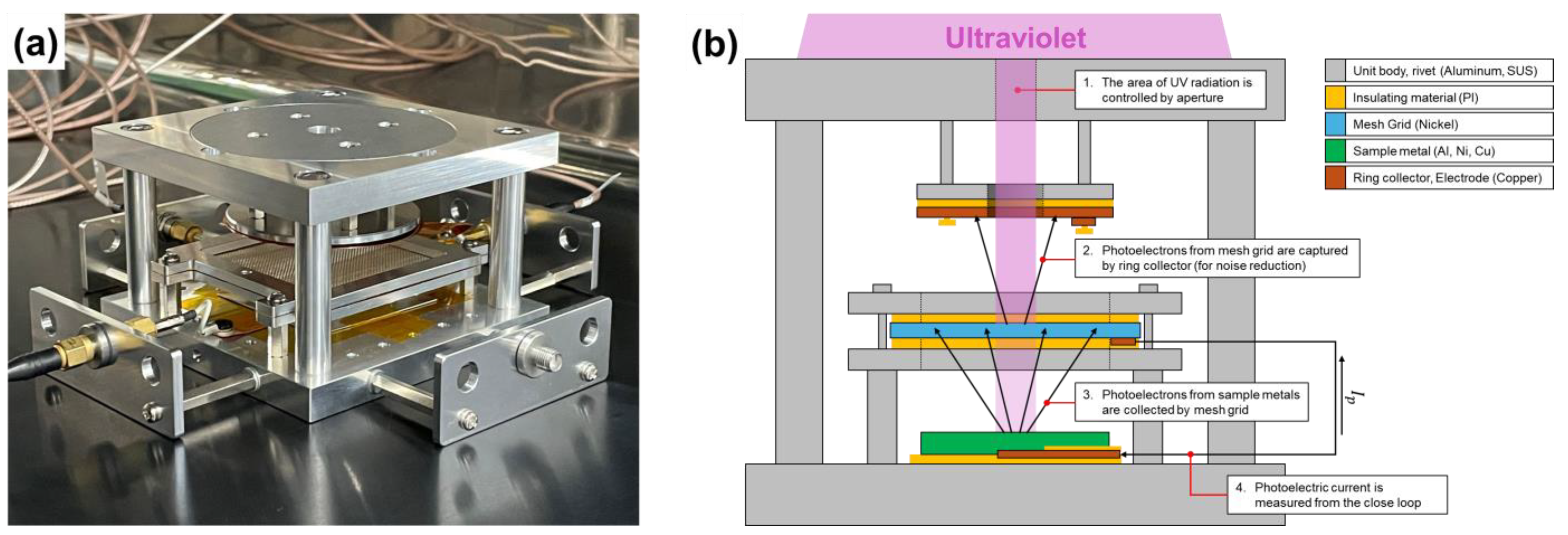
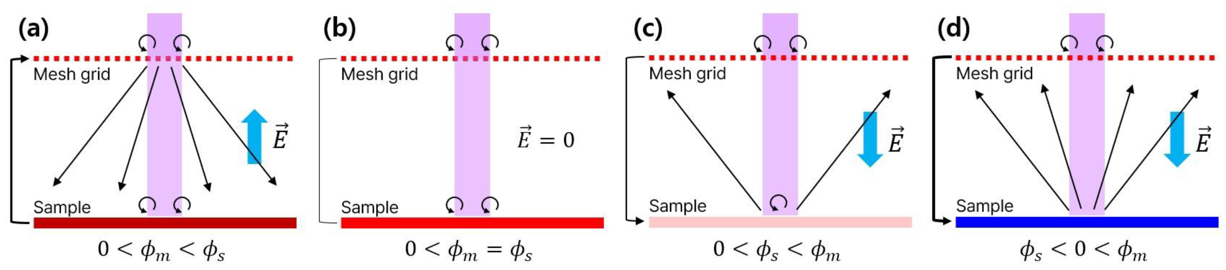
2. The Photoelectric Current Measurement Unit (PCMU)
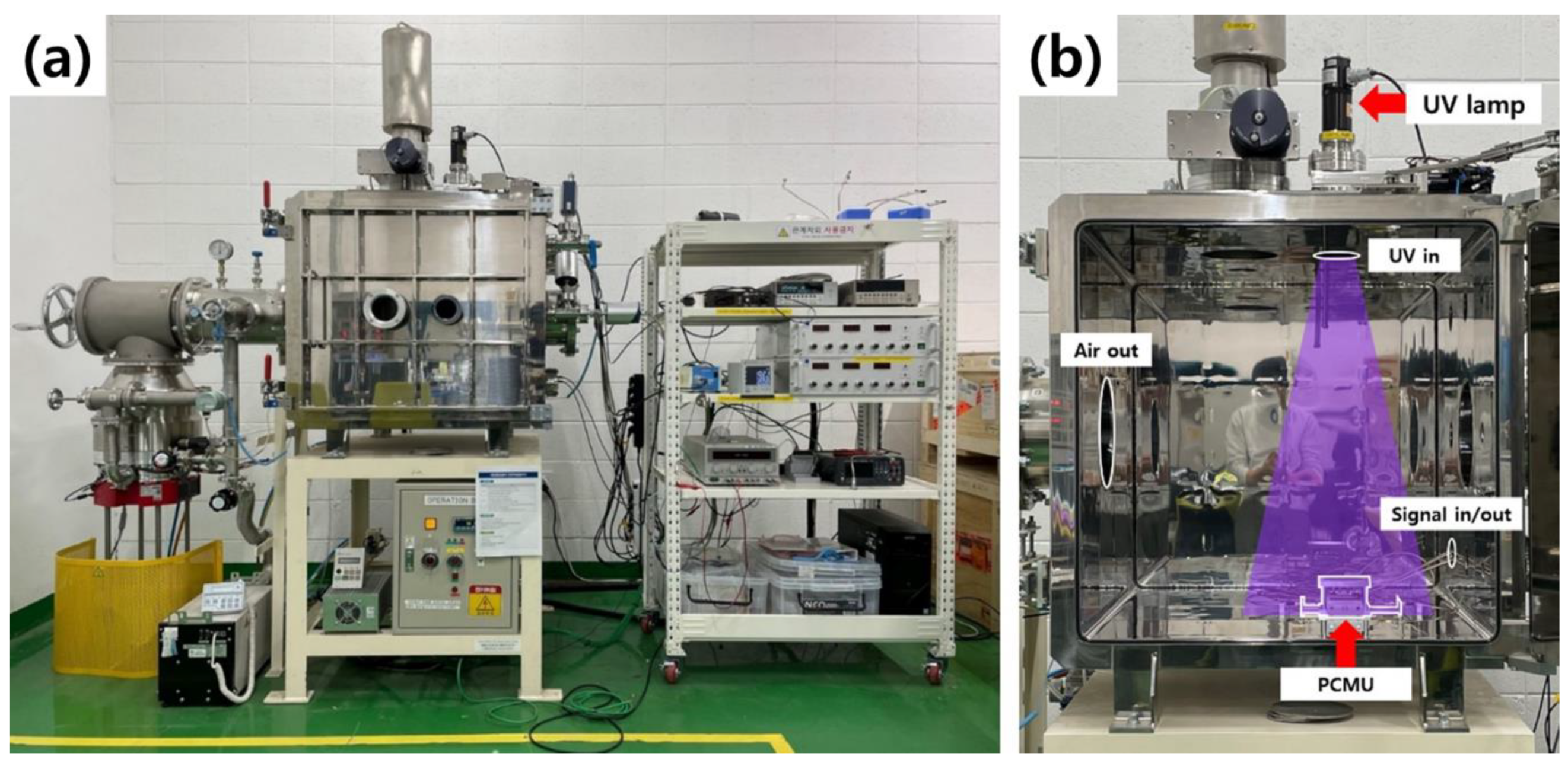
3. Experimental Setup
4. Measurement
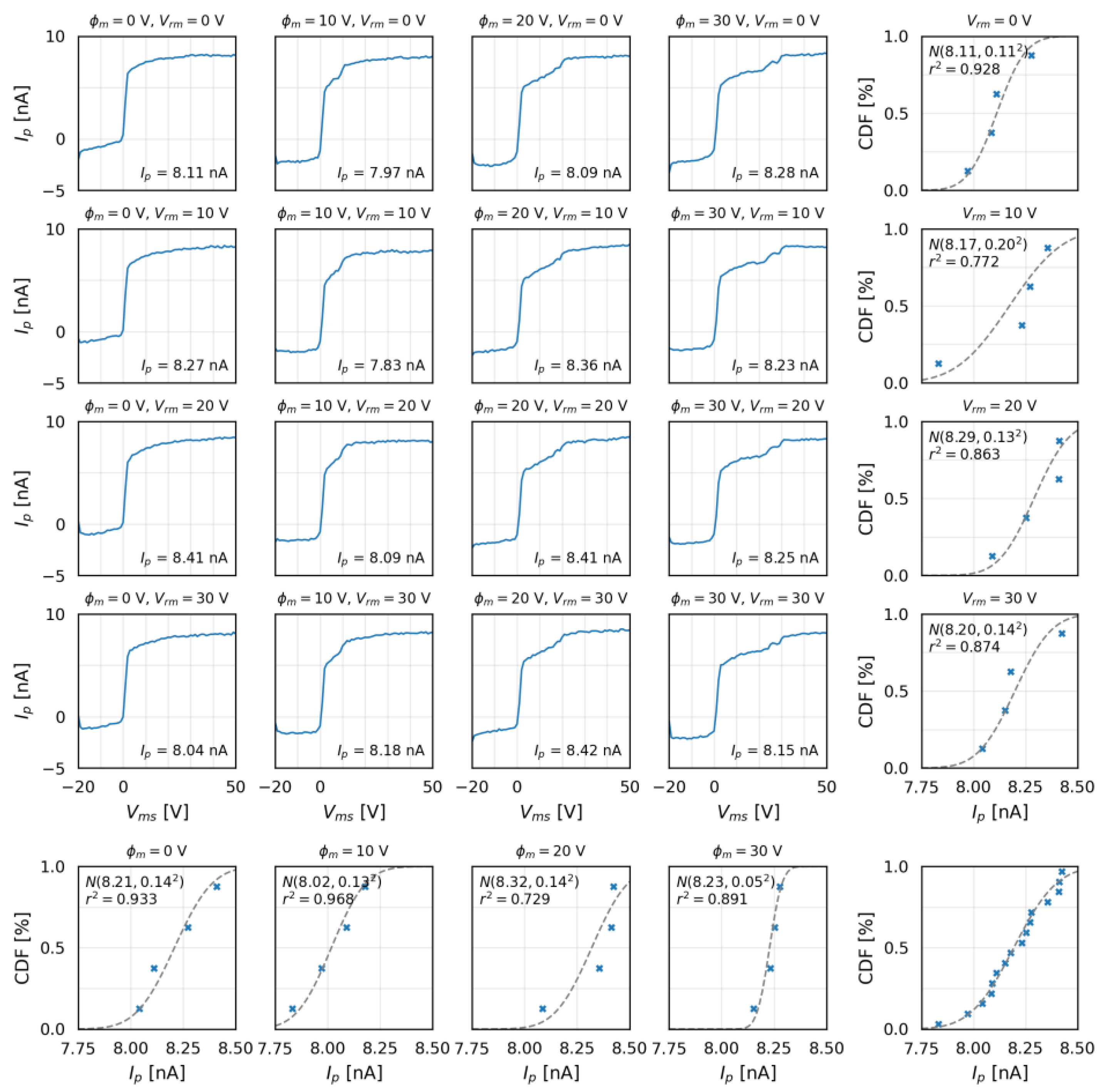
- In the I–V curve, as changed from negative to positive, the current followed the same polarity transition.
- As crossed 0 V, the magnitude of the current rapidly increased.
- As reached the value of , the current slightly increased.
- After exceeded ~40 V, the tended to converge to a certain value.
4.1. Consistency of Measured Values
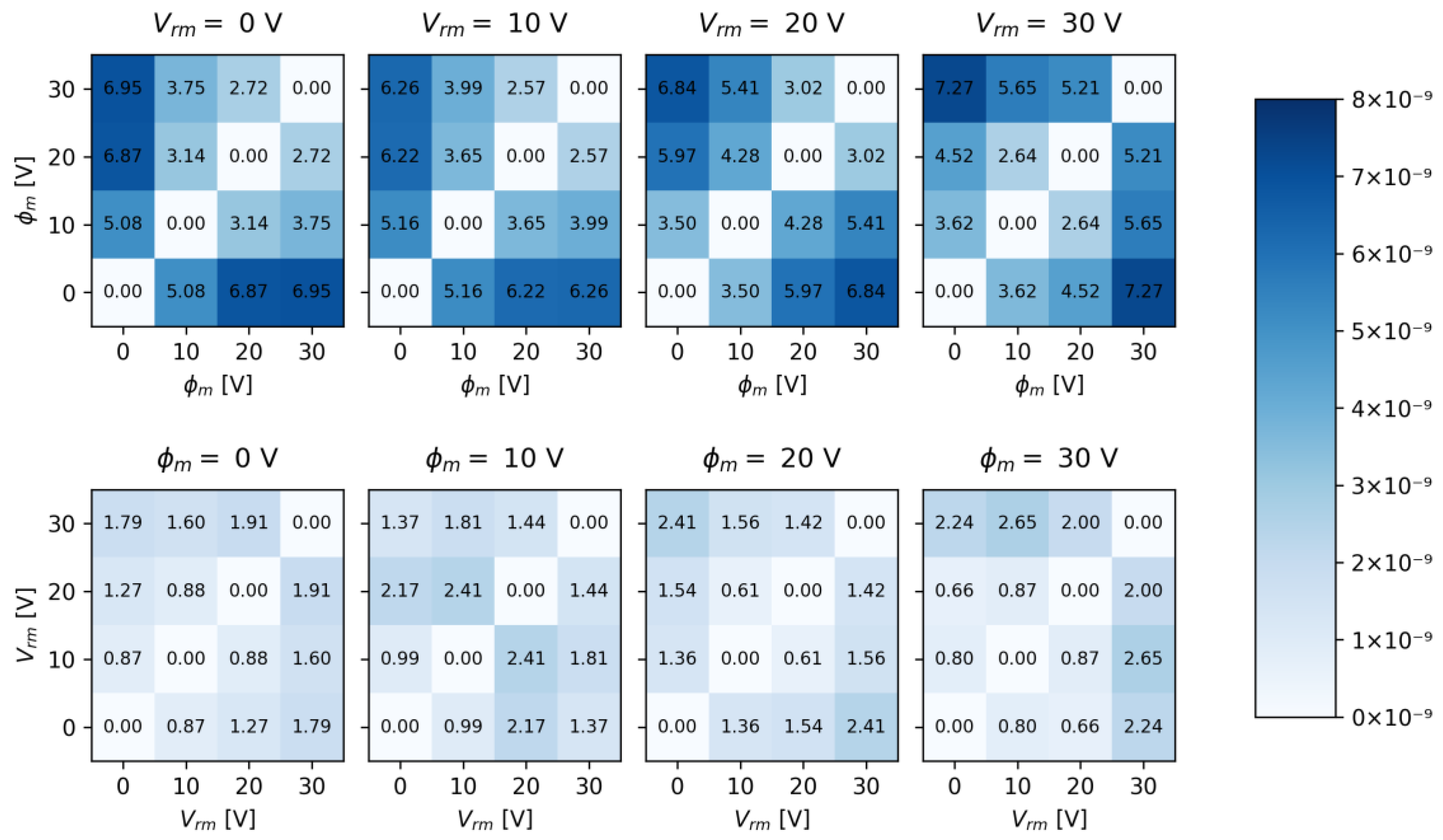
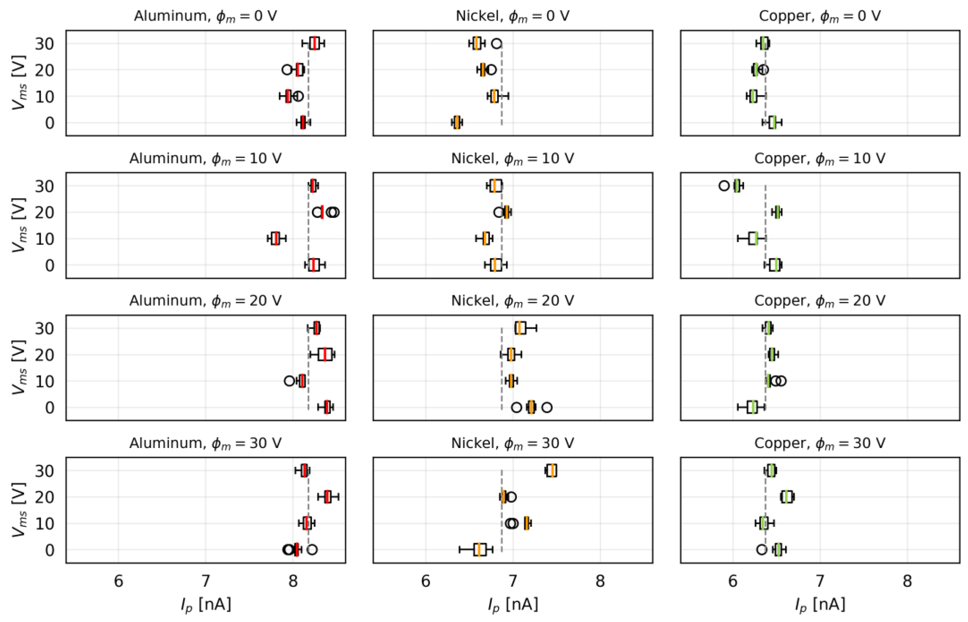
4.2. Effects of and on
4.3. Variation of with Changing
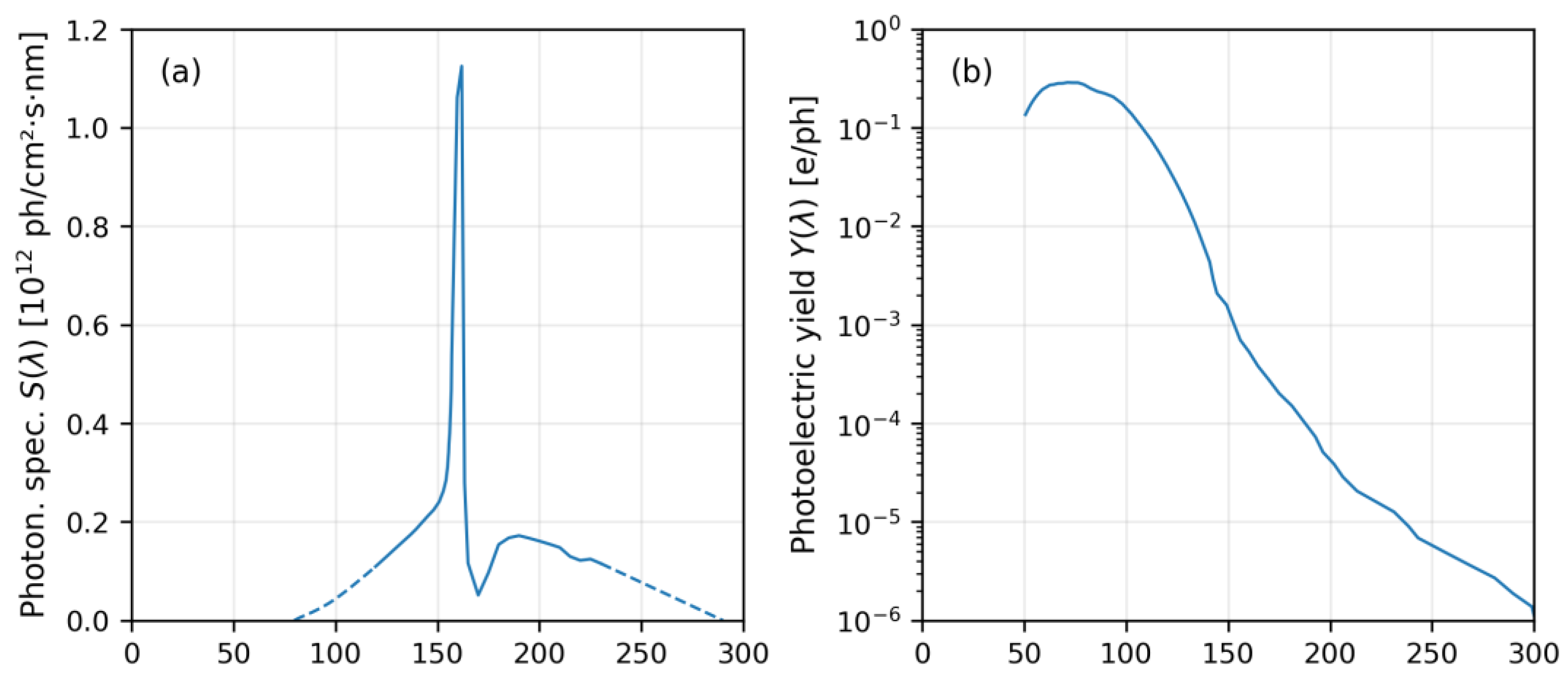
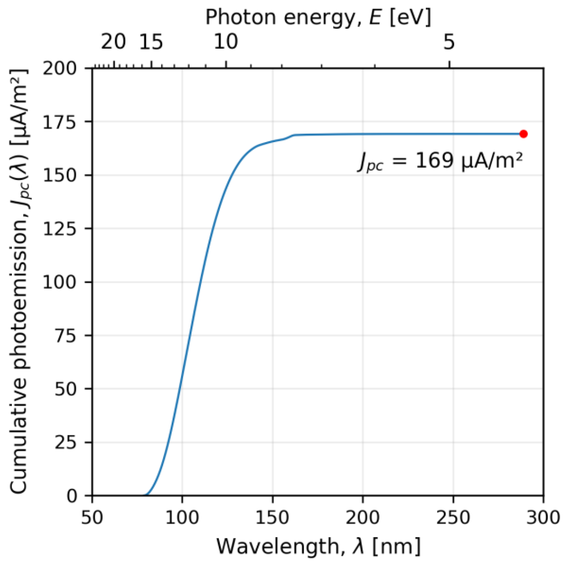
4.4. Photoelectric Current Density Calculation and Method Validation
4.5. Comparison of Measurements for Different Metals
5. Conclusions and Future Work
Author Contributions
Funding
Data Availability Statement
Conflicts of Interest
Abbreviation
| Symbol | Definition |
| The speed of light (299,792,458 m/s) | |
| Elementary charge (2.9 × 10⁻¹⁹ C) | |
| Energy equivalent to a photon with wavelength , | |
| Irradiance spectrum of light source | |
| Differential photoelectron flux, | |
| Planck’s constant (6.626 × 10⁻³⁴ J∙s) | |
| Photoelectron current | |
| Generic current density | |
| Photoelectron current density | |
| Photoelectron current density calculated from experimental setup | |
| Photoelectron current density calculated from measured using PCMU | |
| Normal distribution with mean and standard deviation | |
| Standard deviation of the samples | |
| Photon emission spectrum of light source | |
| Electric potential difference | |
| Electric potential difference between mesh grid and ground, | |
| Electric potential difference between mesh grid and sample metal, | |
| Electric potential difference between ring collector and mesh grid, | |
| Mean of the samples | |
| Photoelectric yield of material | |
| Wavelength | |
| Lower limit of the wavelength range of light source | |
| Upper limit of the wavelength range of light source | |
| Electric potential with respect to electric ground | |
| Electric potential of lunar surface with respect to electric ground | |
| Electric potential of mesh grid with respect to electric ground | |
| Electric potential of sample metal with respect to electric ground | |
| Electric potential of lunar surface electrostatically steady-state condition | |
| Electric potential of ring collector with respect to electric ground | |
| Acronym | Definition |
| CDF | Cumulative distribution function |
| CV | Coefficient of variation, CV = |
| ED | Euclidean distance |
| DTVC | Dirty thermal vacuum chamber |
| KICT | Korea Institute of Civil Engineering and Building Technology |
| PCMU | Photoelectric current measuring unit |
| SED | The sum of Euclidean distances |
| UV | Ultraviolet (10–400 nm) |
| VUV | Vacuum ultraviolet (10–200 nm) |
| WF | Work function |
References
- Ganushkina, N.Y.; Swiger, B.; Dubyagin, S.; Matéo-Vélez, J.-C.; Liemohn, M.W.; Sicard, A.; Payan, D. Worst-Case Severe Environments for Surface Charging Observed at LANL Satellites as Dependent on Solar Wind and Geomagnetic Conditions. Space Weather 2021, 19, e2021SW002732. [Google Scholar] [CrossRef]
- Paul, S.N.; Frueh, C. Space Debris Charging and Its Effect on Orbit Evolution. In Proceedings of the AIAA/AAS Astrodynamics Specialist Conference, Long Beach, CA, USA, 13–16 September 2016; pp. 1–31. [Google Scholar]
- Wang, H.; Phillips, J.R.; Dove, A.R.; Elgohary, T.A. Investigating Particle-Particle Electrostatic Effects on Charged Lunar Dust Transport via Discrete Element Modeling. Adv. Space Res. 2022, 70, 3231–3248. [Google Scholar] [CrossRef]
- Yang, K.; Feng, W.; Xu, L.; Liu, X. Review of Research on Lunar Dust Dynamics. Astrophys. Space Sci. 2022, 367, 67. [Google Scholar] [CrossRef]
- Barker, D.C.; Olivas, A.; Farr, B.; Wang, X.; Buhler, C.R.; Wilson, J.; Mai, J. Adhesion of Lunar Simulant Dust to Materials under Simulated Lunar Environment Conditions. Acta Astronaut. 2022, 199, 25–36. [Google Scholar] [CrossRef]
- Mishra, S.K.; Misra, S. Charging and Dynamics of Dust Particles in Lunar Photoelectron Sheath. Phys. Plasmas 2019, 26, 053703. [Google Scholar] [CrossRef]
- Mishra, S.K.; Bhardwaj, A. Photoelectron Sheath on Lunar Sunlit Regolith and Dust Levitation. Astrophys. J. 2019, 884, 5. [Google Scholar] [CrossRef]
- Wang, X.; Schwan, J.; Hsu, H.-W.; Grün, E.; Horányi, M. Dust Charging and Transport on Airless Planetary Bodies. Geophys. Res. Lett. 2016, 43, 6103–6110. [Google Scholar] [CrossRef]
- Ding, N.; Wang, J. Polansky Measurement of Dust Charging on a Lunar Regolith Simulant Surface. IEEE Trans. Plasma Sci. 2013, 41, 3498–3504. [Google Scholar] [CrossRef]
- Tankosic, D.; Abbas, M.M. Laboratory Studies of Charging Properties of Dust Grains in Astrophysical/Planetary Environments. J. Phys. Conf. Ser. 2012, 399, 012024. [Google Scholar] [CrossRef]
- Wells, I.; Bussey, J.; Swets, N.; Leachman, J. Lunar Dust Removal and Material Degradation from Liquid Nitrogen Sprays. Acta Astronaut. 2023, 206, 30–42. [Google Scholar] [CrossRef]
- Bitetti, G.; Marchetti, M.; Mileti, S.; Valente, F.; Scaglione, S. Degradation of the Surfaces Exposed to the Space Environment. Acta Astronaut. 2007, 60, 166–174. [Google Scholar] [CrossRef]
- Dever, J.; Banks, B.; de Groh, K.; Miller, S. Degradation of Spacecraft Materials. In Handbook of Environmental Degradation of Materials; Kutz, M., Ed.; William Andrew Publishing: Norwich, NY, USA, 2005; pp. 465–501. ISBN 978-0-8155-1500-5. [Google Scholar]
- Payan, D. Payan Electrostatic Behaviour of Materials in a Charging Space Environment. In Proceedings of the 2004 IEEE International Conference on Solid Dielectrics, 2004. ICSD 2004, Toulouse, France, 5–9 July 2004; Volume 2, pp. 917–927. [Google Scholar]
- McCollum, M.; Kim, L.; Lowe, C. Electromagnetic Compatibility Considerations for International Space Station Payload Developers. In Proceedings of the 2020 IEEE Aerospace Conference, Big Sky, MT, USA, 7–14 March 2020; pp. 1–9. [Google Scholar]
- Stubbs, T.J.; Halekas, J.S.; Farrell, W.M.; Vondrak, R.R. Lunar Surface Charging: A Global Perspective Using Lunar Prospector Data; Krueger, H., Graps, A., Eds.; University of California: Berkeley, CA, USA, 2007; Volume 643, pp. 181–184. [Google Scholar]
- Stubbs, T.J.; Farrell, W.M.; Halekas, J.S.; Burchill, J.K.; Collier, M.R.; Zimmerman, M.I.; Vondrak, R.R.; Delory, G.T.; Pfaff, R.F. Dependence of Lunar Surface Charging on Solar Wind Plasma Conditions and Solar Irradiation. Planet. Space Sci. 2014, 90, 10–27. [Google Scholar] [CrossRef]
- Kruzelecky, R.V.; Murzionak, P.; Burbulea, P.; Mena, M.; Sinclair, I.; Schinn, G.; Cloutis, E.; Communications, M. Dusty Thermal Vacuum (DTVAC) Facility Payloads Operations under Simulated Lunar Environment. In Proceedings of the Earth and Space 2021, Virtually, 19–23 April 2021. [Google Scholar]
- Vakkada Ramachandran, A.; Nazarious, M.I.; Mathanlal, T.; Zorzano, M.-P.; Martín-Torres, J. Space Environmental Chamber for Planetary Studies. Sensors 2020, 20, 3996. [Google Scholar] [CrossRef] [PubMed]
- Craven, P.; Vaughn, J.; Schneider, T.; Norwood, J.; Abbas, M.; Alexander, R. MSFC Lunar Environments Test System (LETS) System Development. In Proceedings of the Third Lunar Regolith Simulant Workshop, Huntsville, AL, USA, 17–20 March 2009. [Google Scholar]
- Wass, P.J.; Hollington, D.; Sumner, T.J.; Yang, F.; Pfeil, M. Effective Decrease of Photoelectric Emission Threshold from Gold Plated Surfaces. Rev. Sci. Instrum. 2019, 90, 064501. [Google Scholar] [CrossRef] [PubMed]
- Hechenblaikner, G.; Ziegler, T.; Biswas, I.; Seibel, C.; Schulze, M.; Brandt, N.; Schöll, A.; Bergner, P.; Reinert, F.T. Energy Distribution and Quantum Yield for Photoemission from Air-Contaminated Gold Surfaces under Ultraviolet Illumination Close to the Threshold. J. Appl. Phys. 2012, 111, 124914. [Google Scholar] [CrossRef]
- Cairns, R.B.; Samson, J.A.R. Photoelectric Yields of Metals in the Vacuum Ultraviolet; GCA Corporation: San Francisco, CA, USA, 1966. [Google Scholar]
- Chen, Y.; Yang, Y.; Huang, G.; Li, H.; Li, C.; Wang, S.; Cheng, Y. Development of Photoelectron Emission Yield Measurement System for Metal Materials. In Proceedings of the 2020 International Conference on Sensing, Measurement & Data Analytics in the era of Artificial Intelligence (ICSMD), Xi’an, China, 15–17 October 2020; pp. 148–151. [Google Scholar]
- Dove, A.; Horanyi, M.; Wang, X.; Piquette, M.; Poppe, A.R.; Robertson, S. Experimental Study of a Photoelectron Sheath. Phys. Plasmas 2012, 19, 043502. [Google Scholar] [CrossRef]
- Sickafoose, A.A.; Colwell, J.E.; Horányi, M.; Robertson, S. Experimental Investigations on Photoelectric and Triboelectric Charging of Dust. J. Geophys. Res. Space Phys. 2001, 106, 8343–8356. [Google Scholar] [CrossRef]
- Sternovsky, Z.; Chamberlin, P.; Horanyi, M.; Robertson, S.; Wang, X. Variability of the Lunar Photoelectron Sheath and Dust Mobility Due to Solar Activity. J. Geophys. Res. Space Phys. 2008, 113, 1–4. [Google Scholar] [CrossRef]
- Feuerbacher, B.; Anderegg, M.; Fitton, B.; Laude, L.D.; Willis, R.F.; Grard, R.J.L. Photoemission from Lunar Surface Fines and the Lunar Photoelectron Sheath. In Proceedings of the Third Lunar Science Conference, Huston, TX, USA, 10–13 January 1972. [Google Scholar]
- Hong, G.-W.; Kim, J.; Shin, H.-S.; Chung, T. Development of Lunar Surface Charging Environment Simulation Chamber. Trans. Korean Soc. Mech. Eng. 2021, 45, 377–387. [Google Scholar] [CrossRef]
- Dove, A.; Horányi, M.; Robertson, S.; Wang, X. Laboratory Investigation of the Effect of Surface Roughness on Photoemission from Surfaces in Space. Planet. Space Sci. 2018, 156, 92–95. [Google Scholar] [CrossRef]
- Baikie, I.D.; Grain, A.C.; Sutherland, J.; Law, J. Ambient Pressure Photoemission Spectroscopy of Metal Surfaces. Appl. Surf. Sci. 2014, 323, 45–53. [Google Scholar] [CrossRef]
- Shechtman, O. The Coefficient of Variation as an Index of Measurement Reliability. In Methods of Clinical Epidemiology; Doi, S.A.R., Williams, G.M., Eds.; Springer: Berlin/Heidelberg, Germany, 2013; pp. 39–49. ISBN 978-3-642-37131-8. [Google Scholar]
- Jalilibal, Z.; Amiri, A.; Castagliola, P.; Khoo, M.B.C. Monitoring the Coefficient of Variation: A Literature Review. Comput. Ind. Eng. 2021, 161, 107600. [Google Scholar] [CrossRef]
- Cheng, L.; Zhu, P.; Sun, W.; Han, Z.; Tang, K.; Cui, X. Time Series Classification by Euclidean Distance-Based Visibility Graph. Phys. A Stat. Mech. Appl. 2023, 625, 129010. [Google Scholar] [CrossRef]
- Colwell, J.E.; Batiste, S.; Horányi, M.; Robertson, S.; Sture, S. Lunar Surface: Dust Dynamics and Regolith Mechanics. Rev. Geophys. 2007, 45. [Google Scholar] [CrossRef]
- Freeman, J.W.; Ibrahim, M. Lunar Electric Fields, Surface Potential and Associated Plasma Sheaths. Moon 1975, 14, 103–114. [Google Scholar] [CrossRef]
- Sodha, M.S.; Mishra, S.K. Lunar Photoelectron Sheath and Levitation of Dust. Phys. Plasmas 2014, 21, 093704. [Google Scholar] [CrossRef]
- Baker, D.J. Rayleigh, the Unit for Light Radiance. Appl. Opt. 1974, 13, 2160–2163. [Google Scholar] [CrossRef] [PubMed]
- Abbas, M.M.; Tankosic, D.; Craven, P.D.; Hoover, R.B.; Taylor, L.A.; Spann, J.F.; Leclair, A.; West, E.A. Measurements of Photoelectric Yields of Individual Lunar Dust Grains. In Proceedings of the Dust in Planetary Systems, Kauai, HI, USA, 26–30 September 2005. [Google Scholar]
- Feuerbacher, B.; Fitton, B. Experimental Investigation of Photoemission from Satellite Surface Materials. J. Appl. Phys. 1972, 43, 1563–1572. [Google Scholar] [CrossRef]
- Angus, H.T. The Significance of Hardness. Wear 1979, 54, 33–78. [Google Scholar] [CrossRef]


| Category | Indicator | Parameter |
|---|---|---|
| Settings | UV lamp | Hamamatsu L11798 (Hamamatsu Photonics K.K., Hamamatsu City, Japan) |
| Sample metal | Aluminum (Nilaco Corp., Tokyo, Japan, 99.5%) | |
| Distance from lamp to sample | 80 cm | |
| Mesh grid | Nickel (opening rate: 65%) | |
| Pressure | <5 × 10⁻⁵ mbar | |
| NPLC (Number of powerline cycles) | 10 | |
| Number of experiments/each condition | 5 | |
| Instruments | Photoelectric current measurement | Keithley 6517B (Keithley Instruments, Cleveland, OH, USA) |
| Potential difference between mesh and sample control | Keithley 6517B (Keithley Instruments, Cleveland, OH, USA) | |
| Mesh grid potential control | GPC 6030D (GW Instek, Xīnběi Shì, Taiwan) | |
| Potential difference between ring collector and mesh control | GPC 6030D (GW Instek, Xīnběi Shì, Taiwan) | |
| Data acquisition (DAQ) | NI-9205 (National Instruments Corporation, Austin, TX, USA) |
| Metals | Mean | Standard Deviation | Coefficient of Variation |
|---|---|---|---|
| Aluminum | 8.17 | 0.172 | 0.0211 |
| Nickel | 6.88 | 0.269 | 0.0391 |
| Copper | 6.38 | 0.152 | 0.0238 |
Disclaimer/Publisher’s Note: The statements, opinions and data contained in all publications are solely those of the individual author(s) and contributor(s) and not of MDPI and/or the editor(s). MDPI and/or the editor(s) disclaim responsibility for any injury to people or property resulting from any ideas, methods, instructions or products referred to in the content. |
© 2024 by the authors. Licensee MDPI, Basel, Switzerland. This article is an open access article distributed under the terms and conditions of the Creative Commons Attribution (CC BY) license (https://creativecommons.org/licenses/by/4.0/).
Share and Cite
Park, S.; Chung, T.; Kim, J.; Ryu, B.; Shin, H. Design and Validation of a Photoelectric Current Measuring Unit for Lunar Daytime Simulation Chamber. Aerospace 2024, 11, 69. https://doi.org/10.3390/aerospace11010069
Park S, Chung T, Kim J, Ryu B, Shin H. Design and Validation of a Photoelectric Current Measuring Unit for Lunar Daytime Simulation Chamber. Aerospace. 2024; 11(1):69. https://doi.org/10.3390/aerospace11010069
Chicago/Turabian StylePark, Seungsoo, Taeil Chung, Jihyun Kim, Byunghyun Ryu, and Hyusoung Shin. 2024. "Design and Validation of a Photoelectric Current Measuring Unit for Lunar Daytime Simulation Chamber" Aerospace 11, no. 1: 69. https://doi.org/10.3390/aerospace11010069
APA StylePark, S., Chung, T., Kim, J., Ryu, B., & Shin, H. (2024). Design and Validation of a Photoelectric Current Measuring Unit for Lunar Daytime Simulation Chamber. Aerospace, 11(1), 69. https://doi.org/10.3390/aerospace11010069