Abstract
Highly charged ions are a well-known tool for the nanostructuring of surfaces. We report on the thickness dependence of nanostructures produced by single 260 keV Xe38+ ions on ultrathin poly(methyl methacrylate) (PMMA) films (1 nm to 60 nm) deposited onto Si substrates. The nanostructures induced by slow highly charged ions are rimless craters with a diameter of around 15 nm, which are roughly independent of the thickness of the films down to layers of about 2 nm. The crater depth and thus the overall crater volume are, however, thickness-dependent, decreasing in size in films thinner than ~25 nm. Our findings indicate that although the potential energy of the highly charged ions is the predominant source of deposited energy, the depth of the excited material contributing to crater formation is much larger than the neutralization depth of the ions, which occurs in the first nanometer of the solid at the projectile velocity employed here. This suggests synergism between kinetic and potential-driven processes in nanostructure formation in PMMA.
1. Introduction
The bombardment of solids by individual energetic ions at sufficiently high deposited energy densities may lead to the ejection or flow of a large volume of atoms near the surface, leading to the formation of nano-sized features such as craters or hillocks. This phenomenon is observed in a broad range of ion energies and charge states, including the keV regime where nuclear stopping dominates [1,2,3,4], the electronic stopping regime of fast MeV-GeV ions [5,6,7,8,9,10,11], or the regime where the potential energy of the projectile is preponderant [12,13,14,15,16]. This last regime occurs when slow highly charged ions (HCIs) are used. The potential energy of an HCI in a charge state Q is the sum of the ionization energies of all released electrons. For slow highly charged ions, the creation of surface nanostructures in different materials has been unequivocally correlated to the potential energy of the ions, with little influence of their kinetic energy [16]. In fact, increasing the ion velocity may increase the threshold potential energy for hillock formation and result in smaller surface features as compared to slower ions [12]. While the effectivity of HCIs for nanostructuring the surfaces of materials is undisputed, a quantitative understanding of the mechanism involved is still lacking, despite recent progress obtained from experiments with ultrathin samples [12,16,17,18,19,20,21]. Powerful simulation techniques such as molecular dynamics, which could help to at least predict structural changes due to HCI impacts, face the problem that it is currently not clear how to treat charge-dependent contributions during energy dissipation [21]. For instance, the fraction of energy that is deposited on the surface, as well as the spatial extent of the affected volume in the target material, is not precisely known. Experimental data on these aspects are key to deepening our understanding and pushing forward the development of theoretical concepts.
The experimental determination of the affected volume is not an easy task, as probing methods are typically very surface-sensitive. Some materials, however, such as polymers, exhibit pits or craters after HCI impacts and are therefore well suited to explore this aspect. Ritter et al. investigated pit formation on the surface of 45 nm-thick poly(methyl methacrylate) films after irradiation with Xeq+ (q = 12–48) with kinetic energies between 0.3 and 4 keV/u [14]. The individual HCI impacts resulted in the formation of pits, i.e., rimless craters, with volumes that increased with the potential energy of the impinging ions after a threshold of around ~7 keV for Xe24+ ions. The kinetic energy of Xe ions with a fixed initial charge state had only a minor effect on the total crater volume but affected the pit shape: i.e., faster ions produced deeper and narrower pits [14]. At the highest charge state of q = 48, crater volumes in PMMA films reached values of around 400 nm3. While, in this case, the directly affected volume could be quantified, the question remains whether (and how) spatial confinement in increasingly thinner layers may affect nanostructure production.
In this respect, polymer films are useful systems, because their thickness can be easily controlled, and they may thus be used to investigate the depth of origin of cratering (i.e., to determine the depth of excited material contributing to the formation of surface nanostructures). This has been previously explored using swift heavy ions as projectiles [9]. Apart from being fundamental aspects, this information is also important for applications of defect engineering of two-dimensional materials such as graphene [17,22,23,24,25], hBN [26], MoS2 [21,27], and WS2 [28] by ion irradiation [29].
In this paper, we address the issues of the effective energy deposition and depth of origin of nanostructures induced by HCIs (260 keV Xe38+) on PMMA surfaces following the evolution of crater dimensions as a function of the polymer thickness (from about 60 nm to ~1 nm). We show that the crater diameter remains nearly the same even in ultrathin films and is thus largely independent of the underlying material. The crater volume (and depth), on the other hand, is thickness-dependent and starts to decrease for films thinner than ~25 nm. This indicates that the depth of origin of crater formation is much larger than the presumed region of potential energy deposition, which is only of the order of a few nanometers.
2. Results
Figure 1 shows AFM images of PMMA films of different thicknesses irradiated with 260 keV Xe38+ ions. Nanostructures are clearly seen on the polymer surface as a result of ion impacts. The features are nano-sized craters without hillocks, as seen previously for PMMA irradiated with Xe HCIs [14]. The morphology of the observed structures is similar for all thicknesses, down to very thin layers of about 2 nm. The efficiency of HCIs in producing craters (the ratio between the number of impact features per unit area and the ion fluence) is also similar for all film thicknesses (70–90%, Figure 2), apart from the case of h = 1 nm. For 1 nm-thick PMMA films, cavities could not be clearly identified. It is noteworthy that individual Xeq+ ions (above a threshold q of +24) can produce pores in 1 nm-thick self-supported carbon membranes, which have polymer-like characteristics [19]. Thus, it is somewhat surprising that holes are not seen in the supported 1 nm-thick films, especially considering that the presence of a substrate may amplify material removal, as seen recently in 2D materials [30]. Of course, the lack of holes in our case could be a visibility issue. The surface topography of the 1 nm PMMA films is characterized by peak-to-peak fluctuations with amplitudes of around 0.5 nm. Thus, even if shallow craters are present, they may be easily obscured by the surface roughness. In addition, the presence of the substrate may allow the relaxation of material from the hot crater walls, which may flow at the polymer/Si interface, diminishing the observed hole depth.
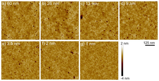
Figure 1.
Representative AFM images of impact features produced by 260 keV Xe38+ highly charged ions on PMMA films. The thickness of the films is given in each image.
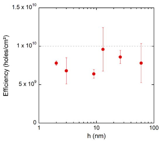
Figure 2.
Ion efficiency as a function of film thickness . The dashed line is the nominal fluence.
We also analyzed the surface of PMMA films irradiated with singly charged Xe ions (260 keV Xe+, Figure 3). At normal incidence, no craters are seen; i.e., kinetic energy deposition alone does not produce craters, as expected (the threshold charge state in 45 nm-thick PMMA is 24+ [14]). On the other hand, impacts of 260 keV Xe+ at 70° incidence (Figure 3c) produce craters on the films due to kinetic sputtering. The cavities seen on the surface in this case are much wider and irregular than those produced by HCIs. Directing collision cascades toward the surface is an efficient way to promote nanostructure formation below the potential energy threshold. In fact, the sputtering yield of PMMA predicted by SRIM 2013 [31] increases by a factor of about 8 when the impact angle changes from 0° to 70° with respect to the surface normal.
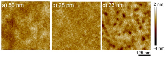
Figure 3.
AFM images of (a) 50 nm- and (b) 28 nm-thick films of PMMA bombarded by 260 keV Xe+ (~1010 ions/cm2) at normal incidence. No evidence of impact craters induced by the ions is seen. (c) Irradiation of a 23 nm-thick film with 260 keV Xe+ at grazing incidence (70° with respect to the surface normal) results in irregular cavities on the surface.
The results of a quantitative analysis of crater dimensions as a function of film thickness are displayed in Figure 4 for two different AFM tip sets. Figure 4a shows that the crater diameter is about 15 nm, independent of the film thickness, even for layers as thin as 2 nm. On the other hand, the crater depth , which is 3 nm in 60 nm-thick films, decreases continuously in thinner films (Figure 4b). Figure 4c shows the crater volume as a function of thickness. For the 60 nm-thick film, is about 200 nm3. This is similar to the volume found by Ritter et al. [14] for 45 nm PMMA thin films using comparable beam conditions. The crater volume becomes smaller as the film thickness diminishes because craters are shallower. For the 2 nm-thick film, the mean crater volume reaches ~80 nm3. It is important to note that the crater depth never reaches the condition (dashed line in Figure 4b), which is the maximum crater depth allowed by the physical size of the layer.
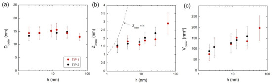
Figure 4.
Average crater dimensions produced by single highly charged ion impacts on PMMA as a function of film thickness for normal incidence: (a) crater diameter , (b) crater depth , and (c) crater volume .
3. Discussion
The potential energy of an HCI is believed to be deposited in a shallow region, which extends only a few nanometers below the surface [10]. Although there is no accurate determination of the neutralization depth of HCIs in polymers, calculations performed for calcium fluoride bombarded by highly charged Xe30+ ions with kinetic energy comparable to that used here point to a neutralization depth of about 4 nm [12]. Thus, considering the prominent effect of potential energy on crater formation by the HCI, the depth of origin of processes leading to cratering would also be expected to be limited to the first nanometers below the surface region. Based on that, only in films thinner than about 5 nm, when the deposition of potential energy is not complete inside the films, would a change in crater volume be expected. Our data, on the other hand, indicate a trend of decreasing crater volume due to much larger thicknesses (~25 nm), suggesting that the depth of origin of the surface nanostructure is significantly larger than what is typically predicted for potential energy deposition. We attribute this “long range” effect to kinetic energy deposition.
Although craters are not produced by the kinetic energy of 260 keV Xe ions alone under normal incidence, collisional events induced by the ions may act synergistically with dense electronic excitations arising from potential energy deposition. Many recoils are produced by the nuclear stopping, but these atoms are either preferentially pushed toward the substrate or become trapped inside the films, as cascades occur with a larger probability in deeper regions. When highly charged ions are used, the topmost layers of the material are removed, allowing the release of atoms from deep layers, which are set into motion by collisional spikes. In this way, craters may eventually become deeper and have larger volumes in thicker films.
We next compare the present results for HCIs to previous data of impact features produced by 923 MeV Pb (electronic energy loss of ~15 keV/nm and equilibrium charge state of ~+45) in ultrathin PMMA films [9]. This offers an opportunity to identify specificities in the mechanism of nanostructure formation in both regimes, considering that the two are associated with high densities of electronic excitation. Clear differences are seen in surface nanostructures induced by swift and slow highly charged ions and their dependence on the thickness of the layer. First, surface features produced by HCIs in PMMA are always rimless cavities, independent of the film thickness (Figure 1). For SHIs, holes are surrounded by well-developed protrusions or rims in thick films. Rim size decreases strongly with decreasing film thickness, but nanostructures produced by SHIs are rimless craters only in ultrathin films [9]. In addition, the crater depth is much larger for SHIs, especially in thick films. On the other hand, the crater diameter for SHIs is, similarly to HCI, almost unaffected by the film thickness, although for sufficiently thin layers below ~10 nm, craters become significantly narrower (by 20–30%). Taken together, such differences indicate that long-range processes are much more relevant for nanostructure formation with SHIs than with HCIs. Excitation from deep layers is especially important for the appearance of hillocks (crater rims) in swift heavy ion impacts.
4. Materials and Methods
Thin films of poly(methyl methacrylate) (PMMA, Polymer Standards, Mw~370,000 u) of thicknesses varying from ~1 nm up to 60 nm were spin-coated from anisole solutions onto Si substrates (with a 2 nm native oxide layer). After deposition, samples were baked at 60 °C for 1 h. The films uniformly covered the Si wafers and depicted a root mean square roughness of around 0.25–0.3 nm for all different thicknesses. Irradiations with 260 keV Xe38+ were performed at the University of Duisburg-Essen using the HICS beamline [32] using fluences of around 1010 ions/cm2. The ion incidence was perpendicular to the surface. For comparison, irradiations with 260 keV Xe+ were also performed in a 500 kV High Voltage Engineering Europe (HVEE) ion implanter at Porto Alegre, Brazil, using angles of incidence of 0° and 70° to the surface normal and fluences of 1010 ions/cm2. The total stopping power of 260 keV Xe ions in PMMA is ~1.85 keV/nm (1.44 keV/nm of nuclear stopping), according to SRIM 2013 [31]. The projected range was close to 160 nm and much larger than the thickness of the thickest film used (60 nm). The potential energy of Xe38+ is about 30 keV.
The size and shape of single-ion impact features and the thicknesses of the samples were characterized by means of scanning probe microscopy with Dimension Icon equipment (Bruker) operated in peak force tapping and standard tapping modes under ambient conditions. Three types of cantilevers were used in the measurements: MPP-12120 (Bruker), with a spring constant of 5 N/m, resonance frequency of 150 kHz, and nominal tip radius of <10 nm; SNL 10 supersharp tips (Bruker), with a spring constant of 0.175 N/m, resonance frequency of 50 kHz, and nominal tip radius of ~2 nm; and RTESPA 300. Images were collected at 1 Hz and 256 scan lines per frame. Special care was taken to use the same tip (or tips of similar quality) to image a set of samples covering all different thicknesses. The tip quality was also checked by scanning a reference sample.
5. Conclusions
Nanostructure production due to individual slow highly charged ion impacts was systematically investigated on PMMA films of various thicknesses to shed light on its depth of origin. The nanostructures induced by Xe38+ ions were rimless craters with a diameter of around 15 nm and a thickness-dependent depth that slightly decreased in films thinner than about 25 nm. This means that excited material lying deeper than 20 nm in the solid seems to contribute to crater production. Thus, our findings indicate that although potential energy is the predominant source of crater formation for HCIs, the depth of excited material contributing to cratering in PMMA is much larger than the expected depth of potential energy deposition at the projectile velocities employed here, most likely due to synergism with kinetic processes triggered by nuclear cascade collisions.
Author Contributions
Conceptualization: R.M.P. and M.S.; methodology, R.S.T., R.M.P. and M.S.; formal analysis, R.S.T. and P.E., data curation, R.S.T. and P.E., writing—original draft preparation, R.S.T. and R.M.P.; writing—review and editing, M.S., P.L.G. and R.M.P.; supervision, R.M.P.; funding acquisition, M.S., P.L.G. and R.M.P. All authors have read and agreed to the published version of the manuscript.
Funding
This research was funded in part by the Coordenação de Aperfeiçoamento de Pessoal de Nível Superior-Brasil (CAPES)-Finance Code 001, by Conselho Nacional de Desenvolvimento Científico e Tecnológico (CNPq) process number 141833/2017-3, and by PRONEX-FAPERGS 16/2551-0000479-0. This work is also funded by the National Institute of Surface Engineering (INCT-INES). P.E. and M.S. acknowledge the German Research Foundation (GFD) by funding through projects SCHL 384/20-1 (Project Number 406129719), C05 (Project Number 278162697) within the SFB1242 “Non-equilibrium Dynamics of Condensed Matter in the Time Domain”.
Institutional Review Board Statement
Not applicable.
Informed Consent Statement
Not applicable.
Data Availability Statement
Not applicable.
Acknowledgments
P.E. and M.S. thank the DFG for supporting the project (SCHL 384/20-1, project number 406 129 719). R.M.P acknowledges the support from Brazilian research agencies CAPES, CNPq, and FAPERGS.
Conflicts of Interest
The authors declare no conflict of interest. The funders had no role in the design of the study; in the collection, analyses, or interpretation of data; in the writing of the manuscript; or in the decision to publish the results.
References
- Donnelly, S.E.; Birtcher, R.C. Heavy ion cratering of gold. Phys. Rev. B 1997, 56, 13599–13602. [Google Scholar] [CrossRef]
- Birtcher, R.C.; Donnelly, S.E.; Schlutig, S. Nanoparticle ejection from Au induced by single Xe ion impacts. Phys. Rev. Lett. 2000, 85, 4968–4971. [Google Scholar] [CrossRef] [PubMed]
- Insepov, Z.; Manory, R.; Matsuo, J.; Yamada, I. Proposal for a hardness measurement technique without indentor by gas-cluster-beam bombardment. Phys. Rev. B 2000, 61, 8744–8752. [Google Scholar] [CrossRef]
- Thibaudau, F.; Cousty, J.; Balanzat, E.; Bouffard, S. Atomic-force-microscopy observations of tracks induced by swift kr ions in mica. Phys. Rev. Lett. 1991, 67, 1582–1585. [Google Scholar] [CrossRef]
- Kopniczky, J.; Reimann, C.T.; Hallen, A.; Sundqvist, B.U.R.; Tengvall, P.; Erlandsson, R. Scanning-force-microscopy study of MeV-atomic-ion-induced surface tracks in organic-crystals. Phys. Rev. B 1994, 49, 625–628. [Google Scholar] [CrossRef]
- Eriksson, J.; Rottler, J.; Reimann, C.T. Fast-ion-induced surface tracks in bioorganic films. Int. J. Mass Spectrom. 1998, 175, 293–308. [Google Scholar] [CrossRef]
- Neumann, R. Scanning probe microscopy of ion-irradiated materials. Nucl. Instrum. Methods Phys. Res. Sect. B-Beam Interact. Mater. At. 1999, 151, 42–55. [Google Scholar] [CrossRef]
- Papaleo, R.M.; Silva, M.R.; Leal, R.; Grande, P.L.; Roth, M.; Schattat, B.; Schiwietz, G. Direct Evidence for Projectile Charge-State Dependent Crater Formation Due to Fast Ions. Phys. Rev. Lett. 2008, 101, 167601. [Google Scholar] [CrossRef]
- Papaléo, R.M.; Thomaz, R.; Gutierres, L.I.; de Menezes, V.M.; Severin, D.; Trautmann, C.; Tramontina, D.; Bringa, E.M.; Grande, P.L. Confinement Effects of Ion Tracks in Ultrathin Polymer Films. Phys. Rev. Lett. 2015, 114, 118302. [Google Scholar] [CrossRef] [PubMed]
- Ochedowski, O.; Osmani, O.; Schade, M.; Bussmann, B.K.; Ban-d’Etat, B.; Lebius, H.; Schleberger, M. Graphitic nanostripes in silicon carbide surfaces created by swift heavy ion irradiation. Nat. Commun. 2014, 5, 8. [Google Scholar] [CrossRef]
- Langer, C.; Ernst, P.; Bender, M.; Severin, D.; Trautmann, C.; Schleberger, M.; Durr, M. Single-ion induced surface modifications on hydrogen-covered Si(001) surfaces-significant difference between slow highly charged and swift heavy ions. New J. Phys. 2021, 23, 093037. [Google Scholar] [CrossRef]
- El-Said, A.; Heller, R.; Meissl, W.; Ritter, R.; Facsko, S.; Lemell, C.; Solleder, B.; Gebeshuber, I.; Betz, G.; Toulemonde, M.; et al. Creation of nanohillocks on CaF2 surfaces by single slow highly charged ions. Phys. Rev. Lett. 2008, 100, 237601. [Google Scholar] [CrossRef] [PubMed]
- Akcoltekin, E.; Peters, T.; Meyer, R.; Duvenbeck, A.; Klusmann, M.; Monnet, I.; Lebius, H.; Schleberger, M. Creation of multiple nanodots by single ions. Nat. Nanotechnol. 2007, 2, 290–294. [Google Scholar] [CrossRef] [PubMed]
- Ritter, R.; Wilhelm, R.; Ginzel, R.; Kowarik, G.; Heller, R.; El-Said, A.; Papaleo, R.; Rupp, W.; Lopez-Urrutia, J.; Ullrich, J.; et al. Pit formation on poly(methyl methacrylate) due to ablation induced by individual slow highly charged ion impact. Europhys. Lett. 2012, 97, 13001. [Google Scholar] [CrossRef]
- Tona, M.; Fujita, Y.; Yamada, C.; Ohtani, S. Electronic interaction of individual slow highly charged ions with TiO2(110). Phys. Rev. B 2008, 77, 155427. [Google Scholar] [CrossRef]
- Aumayr, F.; Facsko, S.; El-Said, A.S.; Trautmann, C.; Schleberger, M. Single ion induced surface nanostructures: A comparison between slow highly charged and swift heavy ions. J. Phys. Condens. Matter 2011, 23, 393001. [Google Scholar] [CrossRef]
- Gruber, E.; Wilhelm, R.A.; Petuya, R.; Smejkal, V.; Kozubek, R.; Hierzenberger, A.; Bayer, B.C.; Aldazabal, I.; Kazansky, A.K.; Libisch, F.; et al. Ultrafast electronic response of graphene to a strong and localized electric field. Nat. Commun. 2016, 7, 13948. [Google Scholar] [CrossRef]
- Creutzburg, S.; Schwestka, J.; Niggas, A.; Inani, H.; Tripathi, M.; George, A.; Heller, R.; Kozubek, R.; Madauss, L.; McEvoy, N.; et al. Vanishing influence of the band gap on the charge exchange of slow highly charged ions in freestanding single-layer MoS2. Phys. Rev. B 2020, 102, 045408. [Google Scholar] [CrossRef]
- Ritter, R.; Wilhelm, R.A.; Stoger-Pollach, M.; Heller, R.; Mucklich, A.; Werner, U.; Vieker, H.; Beyer, A.; Facsko, S.; Golzhauser, A.; et al. Fabrication of nanopores in 1 nm thick carbon nanomembranes with slow highly charged ions. Appl. Phys. Lett. 2013, 102, 063112. [Google Scholar] [CrossRef]
- Wilhelm, R.A.; El-Said, A.S.; Krok, F.; Heller, R.; Gruber, E.; Aumayr, F.; Facsko, S. Highly charged ion induced nanostructures at surfaces by strong electronic excitations. Prog. Surf. Sci. 2015, 90, 377–395. [Google Scholar] [CrossRef][Green Version]
- Kozubek, R.; Tripathi, M.; Ghorbani-Asl, M.; Kretschmer, S.; Madauss, L.; Pollmann, E.; O’Brien, M.; McEvoy, N.; Ludacka, U.; Susi, T.; et al. Perforating Freestanding Molybdenum Disulfide Monolayers with Highly Charged Ions. J. Phys. Chem. Lett. 2019, 10, 904–910. [Google Scholar] [CrossRef] [PubMed]
- Peters, T.; Haake, C.; Hopster, J.; Sokolovsky, V.; Wucher, A.; Schleberger, M. HICS: Highly charged ion collisions with surfaces. Nucl. Instrum. Methods Phys. Res. Sect. B-Beam Interact. Mater. At. 2009, 267, 687–690. [Google Scholar] [CrossRef]
- Hopster, J.; Kozubek, R.; Ban-d’Etat, B.; Guillous, S.; Lebius, H.; Schleberger, M. Damage in graphene due to electronic excitation induced by highly charged ions. Materials 2014, 1, 011011. [Google Scholar] [CrossRef]
- Ernst, P.; Kozubek, R.; Madauss, L.; Sonntag, J.; Lorke, A.; Schleberger, M. Irradiation of graphene field effect transistors with highly charged ions. Nucl. Instrum. Methods Phys. Res. Sect. B-Beam Interact. Mater. At. 2016, 382, 71–75. [Google Scholar] [CrossRef]
- Alzaher, I.; Akcoltekin, S.; Ban-d’Etat, B.; Manil, B.; Dey, K.R.; Been, T.; Boduch, P.; Rothard, H.; Schleberger, M.; Lebius, H. Surface structure modification of single crystal graphite after slow, highly charged ion irradiation. Nucl. Instrum. Methods Phys. Res. Sect. B-Beam Interact. Mater. At. 2018, 420, 23–26. [Google Scholar] [CrossRef]
- Kozubek, R.; Ernst, P.; Herbig, C.; Michely, T.; Schleberger, M. Fabrication of Defective Single Layers of Hexagonal Boron Nitride on Various Supports for Potential Applications in Catalysis and DNA Sequencing. Acs Appl. Nano Mater. 2018, 1, 3765–3773. [Google Scholar] [CrossRef]
- Schwestka, J.; Inani, H.; Tripathi, M.; Niggas, A.; McEvoy, N.; Libisch, F.; Aumayr, F.; Kotakoski, J.; Wilhelm, R.A. Atomic-Scale Carving of Nanopores into a van der Waals Heterostructure with Slow Highly Charged Ions. Acs Nano 2020, 14, 10536–10543. [Google Scholar] [CrossRef]
- Asaithambi, A.; Kozubek, R.; Prinz, G.M.; Reale, F.; Pollmann, E.; Ney, M.; Mattevi, C.; Schleberger, M.; Lorke, A. Laser- and Ion-Induced Defect Engineering in WS2 Monolayers. Phys. Status Solidi-Rapid Res. Lett. 2021, 15, 2000466. [Google Scholar] [CrossRef]
- Schleberger, M.; Kotakoski, J. 2D Material Science: Defect Engineering by Particle Irradiation. Materials 2018, 11, 1885. [Google Scholar] [CrossRef]
- Thomaz, R.; Lima, N.W.; Teixeira, D.; Gutierres, L.I.; Alencar, I.; Trautmann, C.; Grande, P.L.; Papaléo, R.M. Ion tracks in ultrathin polymer films: The role of the substrate. Curr. Appl. Phys. 2021, 32, 91–97. [Google Scholar] [CrossRef]
- Ziegler, J.F.; Ziegler, M.D.; Biersack, J.P. SRIM—The stopping and range of ions in matter (2010). Nucl. Instrum. Methods Phys. Res. Sect. B Beam Interact. Mater. At. 2010, 268, 1818–1823. [Google Scholar] [CrossRef]
- Skopinski, L.; Ernst, P.; Herder, M.; Kozubek, R.; Madauss, L.; Sleziona, S.; Maas, A.; Konigstein, N.; Lebius, H.; Wucher, A.; et al. Time-of-flight mass spectrometry of particle emission during irradiation with slow, highly charged ions. Rev. Sci. Instrum. 2021, 92, 023909. [Google Scholar] [CrossRef] [PubMed]


Publisher’s Note: MDPI stays neutral with regard to jurisdictional claims in published maps and institutional affiliations. |
© 2022 by the authors. Licensee MDPI, Basel, Switzerland. This article is an open access article distributed under the terms and conditions of the Creative Commons Attribution (CC BY) license (https://creativecommons.org/licenses/by/4.0/).