Comparison of Strain Effect between Aluminum and Palladium Gated MOS Quantum Dot Systems


Abstract
1. Introduction
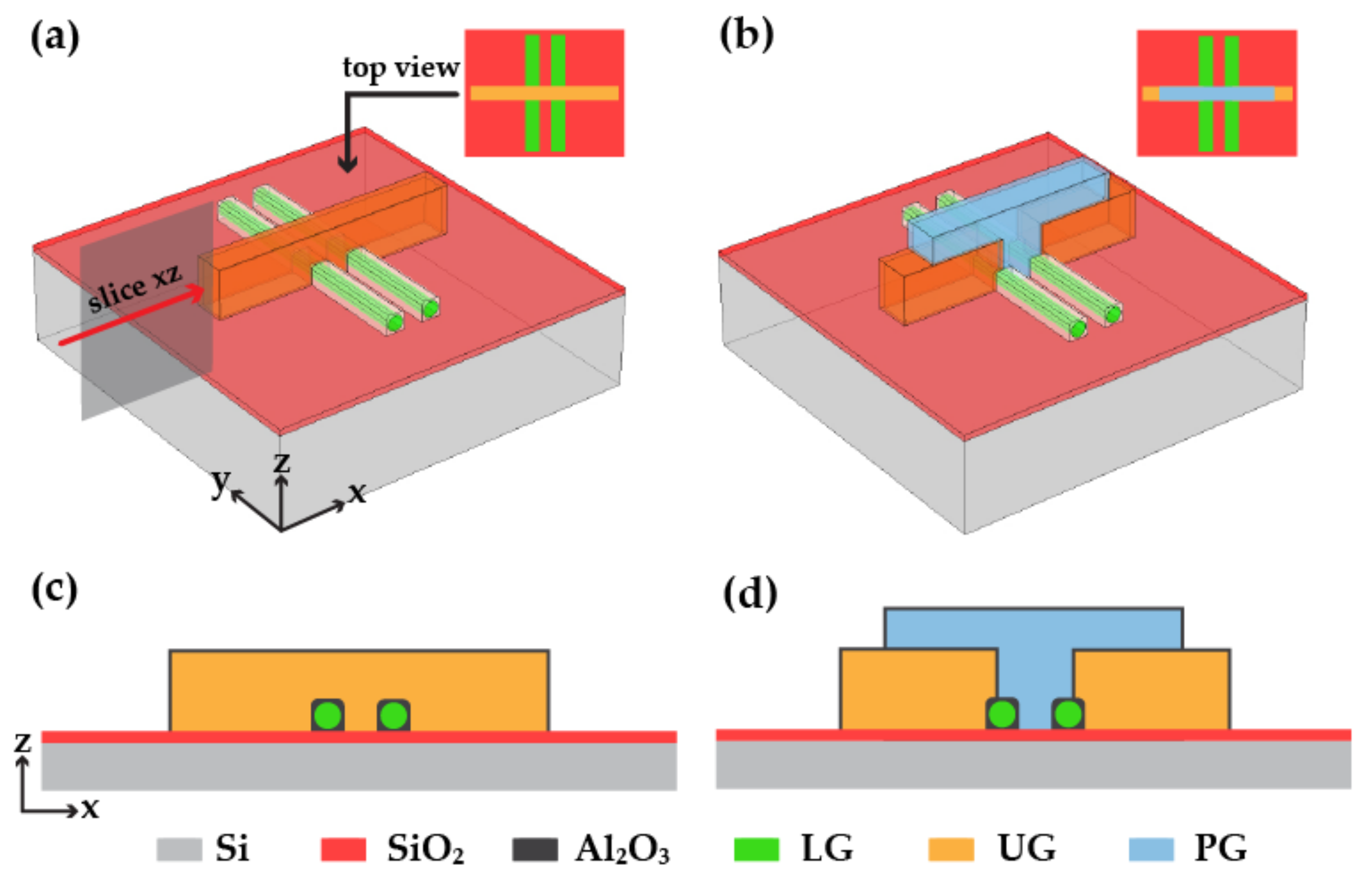
2. Methods
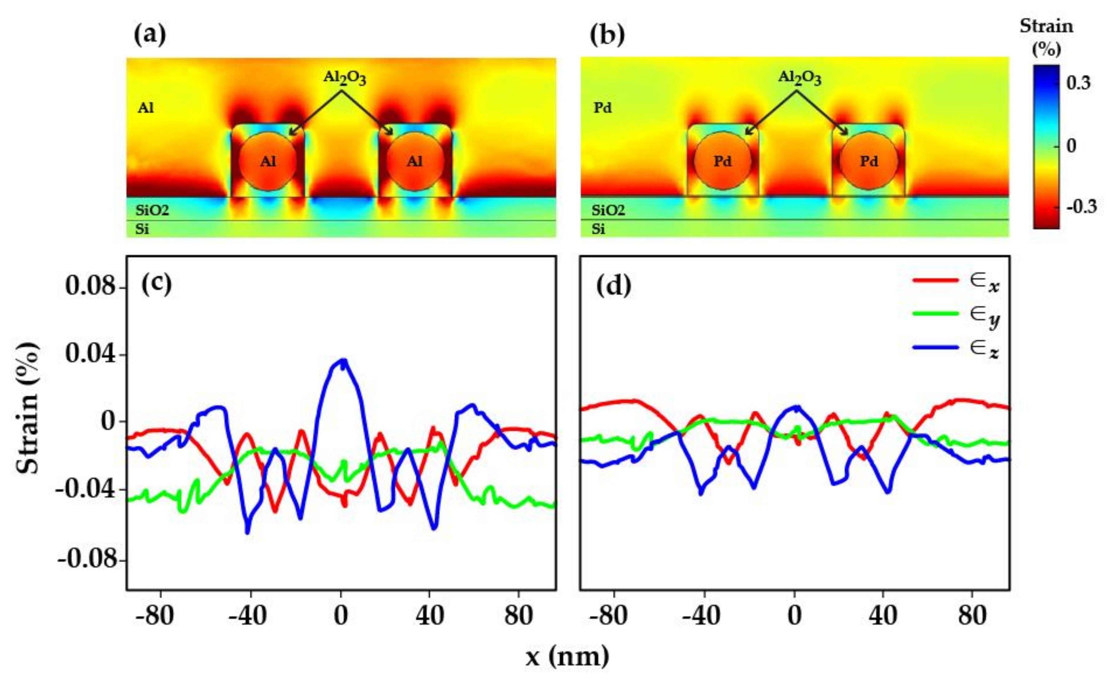
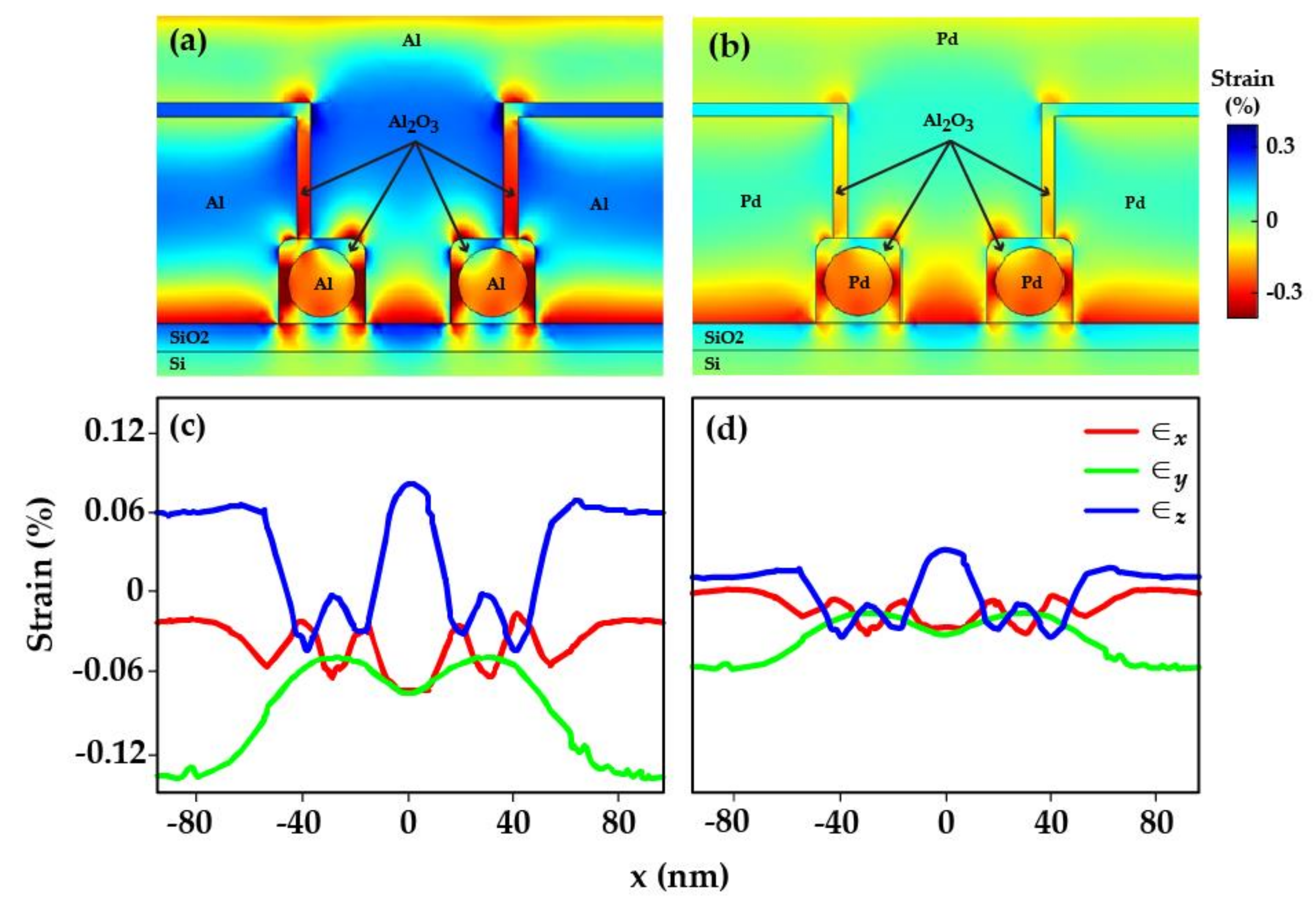
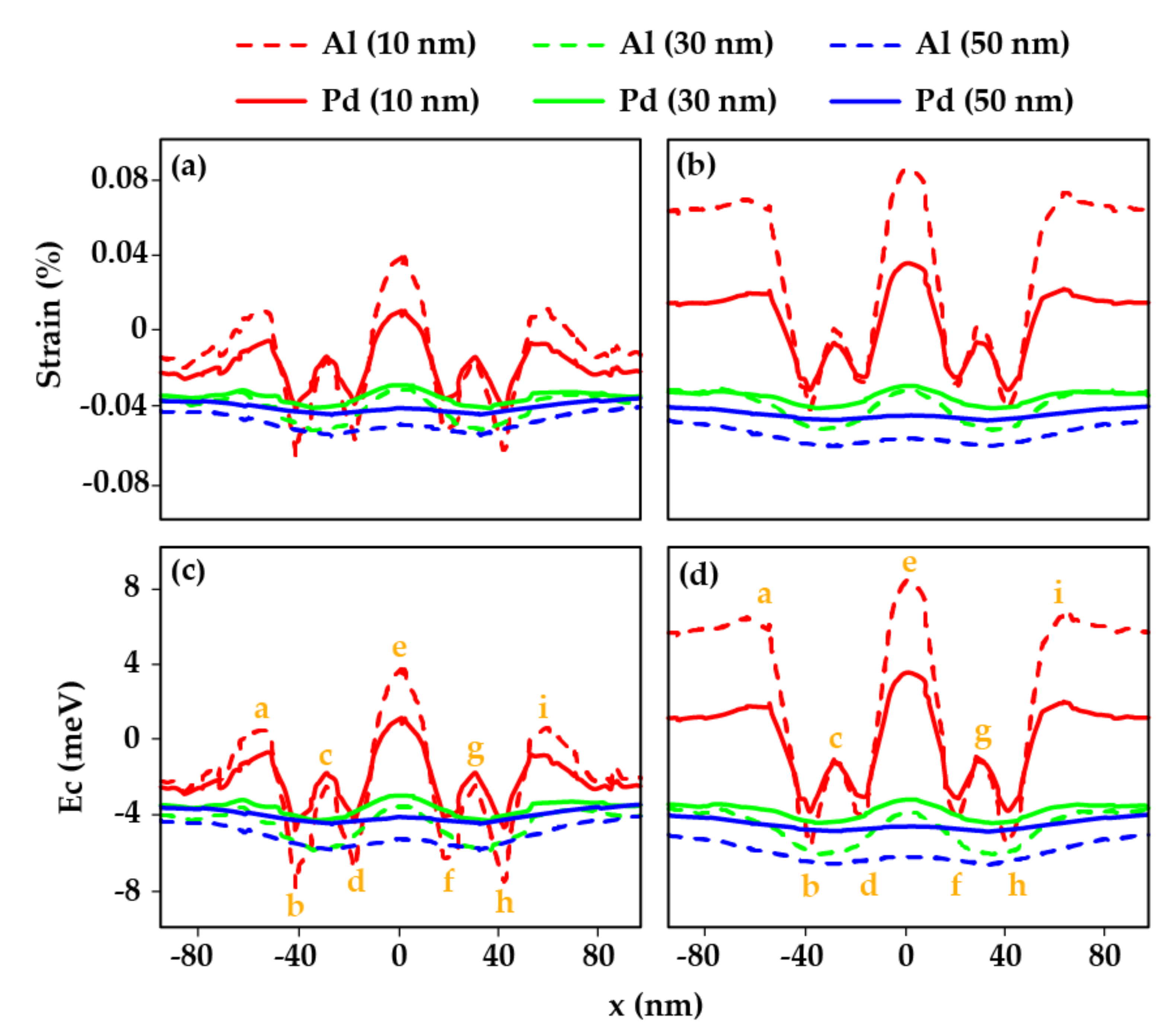
3. Results and Discussion
4. Conclusions
Author Contributions
Funding
Conflicts of Interest
References
- Loss, D.; DiVincenzo, D.P. Quantum computation with quantum dots. Phys. Rev. A 1998, 57, 120–126. [Google Scholar] [CrossRef]
- Angus, S.J.; Ferguson, A.J.; Dzurak, A.S.; Clark, R.G. Gate-defined quantum dots in intrinsic silicon. Nano Lett. 2007, 7, 2051–2055. [Google Scholar] [CrossRef] [PubMed]
- Lim, W.H.; Zwanenburg, F.A.; Huebl, H.; Möttönen, M.; Chan, K.W.; Morello, A.; Dzurak, A.S. Observation of the single-electron regime in a highly tunable silicon quantum dot. Appl. Phys. Lett. 2009, 95, 242102. [Google Scholar] [CrossRef]
- Tracy, L.A.; Nordberg, E.P.; Young, R.W.; Borras Pinilla, C.; Stalford, H.L.; Ten Eyck, G.A.; Eng, K.; Childs, K.D.; Wendt, J.R.; Grubbs, R.K.; et al. Double quantum dot with tunable coupling in an enhancement-mode silicon metal-oxide semiconductor device with lateral geometry. Appl. Phys. Lett. 2010, 97, 192110. [Google Scholar] [CrossRef]
- Lai, N.S.; Lim, W.H.; Yang, C.H.; Zwanenburg, F.A.; Coish, W.A.; Qassemi, F.; Morello, A.; Dzurak, A.S. Pauli spin blockade in a highly tunable silicon double quantum dot. Sci. Rep. 2011, 1, 110. [Google Scholar] [CrossRef]
- Yang, C.H.; Rossi, A.; Ruskov, R.; Lai, N.S.; Mohiyaddin, F.A.; Lee, S.; Tahan, C.; Klimeck, G.; Morello, A.; Dzurak, A.S. Spin-valley lifetimes in a silicon quantum dot with tunable valley splitting. Nat. Commun. 2013, 4, 2069. [Google Scholar] [CrossRef]
- Liles, S.D.; Li, R.; Yang, C.H.; Hudson, F.E.; Veldhorst, M.; Dzurak, A.S.; Hamilton, A.R. Spin and orbital structure of the first six holes in a silicon metal-oxide-semiconductor quantum dot. Nat. Commun. 2018, 9, 3255. [Google Scholar] [CrossRef]
- Thorbeck, T.; Zimmerman, N.M. Formation of strain-induced quantum dots in gated semiconductor nanostructures. AIP Adv. 2015, 5, 087107. [Google Scholar] [CrossRef]
- Fang, W.; Lo, C.Y. On the thermal expansion coefficients of thin films. Sens. Actuators A: Phys. 2000, 84, 310–314. [Google Scholar] [CrossRef]
- Maune, B.M.; Borselli, M.G.; Huang, B.; Ladd, T.D.; Deelman, P.W.; Holabird, K.S.; Kiselev, A.A.; Alvarado-Rodriguez, I.; Ross, R.S.; Schmitz, A.E.; et al. Coherent singlet-triplet oscillations in a silicon-based double quantum dot. Nature 2012, 481, 344–347. [Google Scholar] [CrossRef]
- Ono, K.; Mori, T.; Moriyama, S. High-temperature operation of a silicon qubit. Sci. Rep. 2019, 9, 469. [Google Scholar] [CrossRef] [PubMed]
- Brauns, M.; Amitonov, S.V.; Spruijtenburg, P.C.; Zwanenburg, F.A. Palladium gates for reproducible quantum dots in silicon. Sci. Rep. 2018, 8, 5690. [Google Scholar] [CrossRef] [PubMed]
- Nordberg, E.P.; Stalford, H.L.; Young, R.; Ten Eyck, G.A.; Eng, K.; Tracy, L.A.; Childs, K.D.; Wendt, J.R.; Grubbs, R.K.; Stevens, J.; et al. Charge sensing in enhancement mode double-top-gated metal-oxide-semiconductor quantum dots. Appl. Phys. Lett. 2009, 90, 202102. [Google Scholar] [CrossRef]
- Baptista, A.; Silva, F.; Porteiro, J.; Míguez, J.; Pinto, G. Sputtering physical vapour deposition (PVD) coatings: A critical review on process improvement and market trend demands. Coatings 2018, 8, 402. [Google Scholar] [CrossRef]
- Rossi, A.; Tanttu, T.; Hudson, F.E.; Sun, Y.; Möttönen, M.; Dzurak, A.S. Silicon metal-oxide-semiconductor quantum dots for single-electron pumping. J. Vis. Exp. 2015, 100, 52852. [Google Scholar] [CrossRef] [PubMed]
- German, R.M. Sintering simplified: Surface area, density, and grain size relations. Mater. Sci. Forum 2016, 835, 50–75. [Google Scholar] [CrossRef]
- Spruijtenburg, P.C.; Amitonov, S.V.; Mueller, F.; van der Wiel, W.G.; Zwanenburg, F.A. Passivation and charaterization of charge defects in ambipolar silicon quantum dot. Sci. Rep. 2016, 6, 38127. [Google Scholar] [CrossRef]
- Pla, J.J.; Tan, K.Y.; Dehollain, J.P.; Lim, W.H.; Morton, J.J.L.; Jamieson, D.N.; Dzurak, A.S.; Morello, A. A single-atom electron spin qubit in silicon. Nature 2012, 489, 541–545. [Google Scholar] [CrossRef]
- Huebl, H.; Stegner, A.R.; Stutzmann, M.; Brandt, M.S.; Vogg, G.; Bensch, F.; Rauls, E.; Gerstmann, U. Phosphorus donors in highly strained silicon. Phys. Rev. Lett. 2006, 97, 1–4. [Google Scholar] [CrossRef]
- Al-Mufti, W.M.; Hashim, U.; Tijjani, A. Current trend in simulation: Review nanostructures using comsol multiphysics. J. Appl. Sci. Res. 2012, 8, 5579–5582. [Google Scholar]
- Migwi, C.M.; Darby, M.I.; Wostenholm, G.H.; Yates, B.; Moss, M.; Duffy, R. A method of determining the shear modulus and Poisson’s ratio of polymer materials. J. Mater. Sci. 1994, 29, 3430–3432. [Google Scholar] [CrossRef]
- White, G.K.; Pawlowicz, A.T. Thermal expansion of rhodium, iridium, and palladium at low temperatures. J. Low Temp. Phys. 1970, 2, 631–639. [Google Scholar] [CrossRef]
- Eriguchi, K.; Harada, Y.; Niwa, M. Influence of 1 nm-thick structural “strained-layer” near SiO2//Si interface on sub-4 nm-thick gate oxide reliability. In Proceedings of the International Electron Devices Meeting 1998, Technical Digest, San Francisco, CA, USA, 6–9 December 1998. [Google Scholar]
- Fischetti, M.V.; Laux, S.E. Band structure, deformation potentials, and carrier mobility in strained Si, Ge, and SiGe alloys. J. Appl. Phys. 1996, 80, 2234. [Google Scholar] [CrossRef]
- Jellison, G.E., Jr. Examination of thin SiO2 films on Si using spectroscopic polarization modulation ellipsometry. J. Appl. Phys. 1991, 69, 7627. [Google Scholar] [CrossRef]
- Xu, Y.B.; Yang, H.G. Capacitance extraction method for a gate-induced quantum dot in silicon nanowire metal–oxide–semiconductor field-effect transistors. Chin. Phys. B 2017, 26, 127302. [Google Scholar] [CrossRef]


| Material | Density, ρ (kg/m3) | Young’s Modulus, E (GPa) | Poisson’s Ratio, v (kg/m3) | Coefficient of Thermal Expansion, α (× 10−6/K) | Reference |
|---|---|---|---|---|---|
| Palladium | 12,020 | 73 | 0.44 | 11.8 | [22] |
| Aluminum | 2700 | 70 | 0.35 | 23 | [8] |
| Aluminum Oxide | 3900 | 300 | 0.22 | 5.4 | |
| Silicon | 2300 | 130 | 0.27 | 2.6 | |
| Silicon Dioxide | 2200 | 73 | 0.17 | 0.49 |
| SiO2 (nm) | |a| + |b| (meV) | |d| +|e| (meV) | |e| + |f| (meV) | |h| + |i| (meV) | Average (meV) |
|---|---|---|---|---|---|
| 10 - Al | 7.90 | 9.92 | 10.6 | 8.57 | 9.25 |
| 10 - Pd | 5.22 | 5.12 | 5.55 | 5.24 | 5.28 |
| ∆ 10 (Al-Pd) | 2.68 | 4.8 | 4.95 | 3.33 | 3.97 |
| 30 - Al | 1.39 | 1.71 | 1.87 | 1.32 | 1.57 |
| 30 - Pd | 0.52 | 0.98 | 1.08 | 0.64 | 0.81 |
| ∆ 30 (Al-Pd) | 0.87 | 0.73 | 0.79 | 0.68 | 0.76 |
| 50 - Al | 0.92 | 0.45 | 0.19 | 0.95 | 0.63 |
| 50 - Pd | 0.5 | 0.28 | 0.12 | 0.52 | 0.36 |
| ∆ 50 (Al-Pd) | 0.42 | 0.17 | 0.07 | 0.43 | 0.27 |
| SiO2 (nm) | |a| + |b| (meV) | |d| +|e| (meV) | |e| + |f| (meV) | |h| + |i| (meV) | Average (meV) |
|---|---|---|---|---|---|
| 10 - Al | 12.06 | 12.25 | 12.49 | 10.88 | 11.92 |
| 10 - Pd | 5.71 | 6.52 | 6.61 | 4.92 | 5.94 |
| ∆ 10 (Al-Pd) | 6.35 | 5.73 | 5.88 | 5.96 | 5.98 |
| 30 - Al | 1.92 | 1.47 | 1.28 | 1.00 | 2.84 |
| 30 - Pd | 0.84 | 0.84 | 0.69 | 0.51 | 0.72 |
| ∆ 30 (Al-Pd) | 1.08 | 0.63 | 0.59 | 0.49 | 2.12 |
| 50 - Al | 0.53 | 0.2 | 0.23 | 0.42 | 0.35 |
| 50 - Pd | 0.26 | 0.12 | 0.13 | 0.21 | 0.18 |
| ∆ 50 (Al-Pd) | 0.27 | 0.08 | 0.10 | 0.21 | 0.17 |
© 2020 by the authors. Licensee MDPI, Basel, Switzerland. This article is an open access article distributed under the terms and conditions of the Creative Commons Attribution (CC BY) license (http://creativecommons.org/licenses/by/4.0/).
Share and Cite
Mooy, B.C.H.; Tan, K.Y.; Lai, N.S. Comparison of Strain Effect between Aluminum and Palladium Gated MOS Quantum Dot Systems. Universe 2020, 6, 51. https://doi.org/10.3390/universe6040051
Mooy BCH, Tan KY, Lai NS. Comparison of Strain Effect between Aluminum and Palladium Gated MOS Quantum Dot Systems. Universe. 2020; 6(4):51. https://doi.org/10.3390/universe6040051
Chicago/Turabian StyleMooy, Brian Chi Ho, Kuan Yen Tan, and Nai Shyan Lai. 2020. "Comparison of Strain Effect between Aluminum and Palladium Gated MOS Quantum Dot Systems" Universe 6, no. 4: 51. https://doi.org/10.3390/universe6040051
APA StyleMooy, B. C. H., Tan, K. Y., & Lai, N. S. (2020). Comparison of Strain Effect between Aluminum and Palladium Gated MOS Quantum Dot Systems. Universe, 6(4), 51. https://doi.org/10.3390/universe6040051