
Effect of Annealing Temperature on Radio Frequency Sputtered p-Type Delafossite Copper Chromium Oxide (CuCrO2) Thin Films and Investigation of Diode Characteristics Forming Transparent pn-Heterojunction

Abstract
1. Introduction
2. Experimental Section
3. Results and Discussion

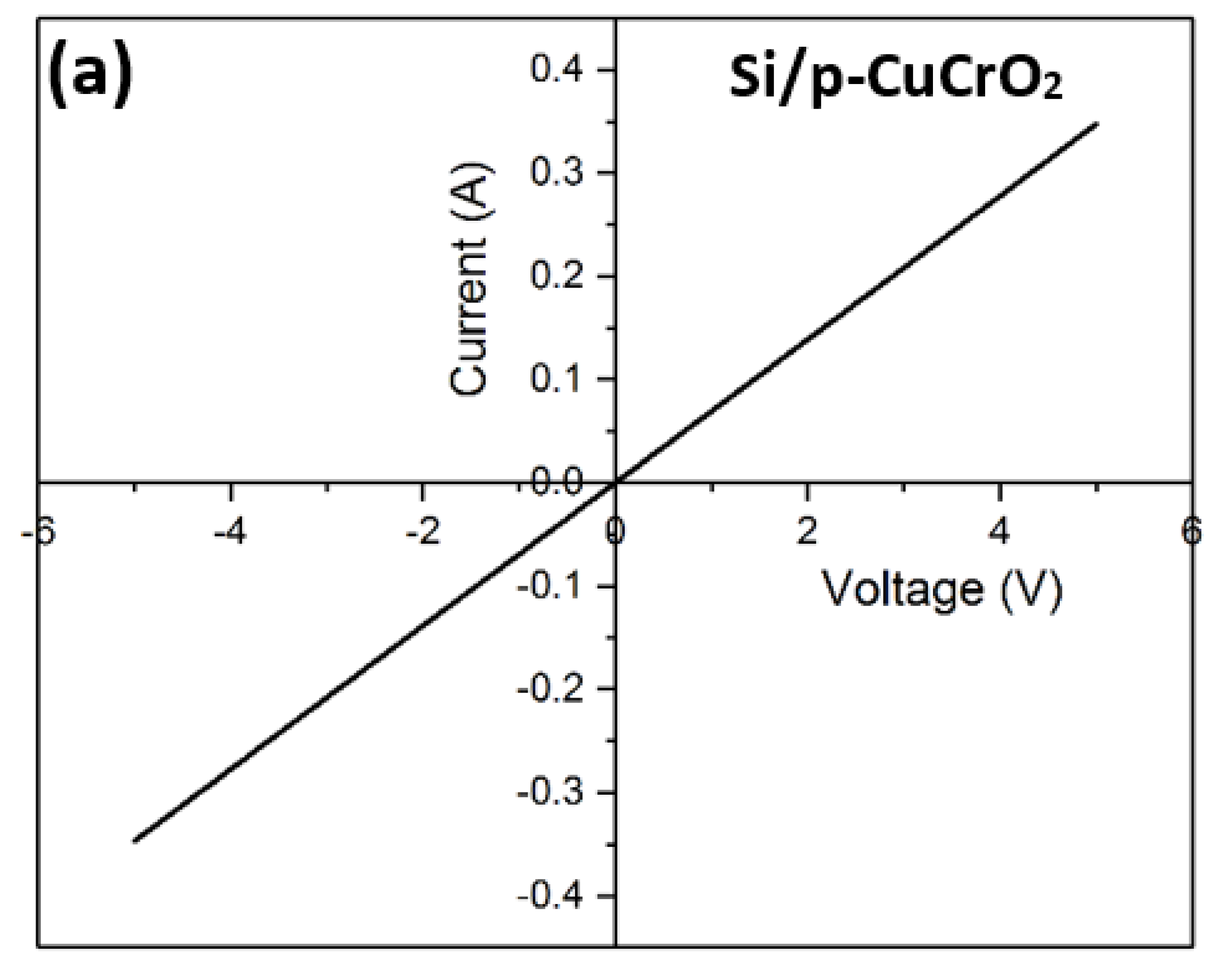
| Diode | Turn ON Voltage (V) | Leakage Current (A) | Rectification Ratio | Ideality Factor | Reference |
|---|---|---|---|---|---|
| D1 | 0.85 | 1.24 × 10⁻⁸ (at 0.9 V) | 2375 (at 2 V) | 4.13 | This work |
| D2 | 1.29 | 2.15 × 10⁻⁸ (at 0.9 V) | 1664 (at 1.8 V) | 5.8 | This work |
| n-ITO/p-CuCrO2 | ~0.87 | NR | >104 | 3.90 | [49] |
| n-ZnO/p-Cu0.66Cr1.33O2 | 1.40 | NR | 13 | 6.30 | [90] |
| n-ZnO/p-Mg:CuCrO2 | ~2.00 | NR | ~7–10 | NR | [91] |
| n-ZnO/p-CuCrO2 | NR | NR | 107 | 1.56 | [92] |
| n-ZnO/p-CuCrO2 | NR | NR | 20 | 2.20 | [93] |
4. Conclusions
Author Contributions
Funding
Institutional Review Board Statement
Informed Consent Statement
Data Availability Statement
Acknowledgments
Conflicts of Interest
References
- Hu, L.; Wei, R.H.; Tang, X.W.; Lu, W.J.; Zhu, X.B.; Sun, Y.P. Design strategy for p-type transparent conducting oxides. J. Appl. Phys. 2020, 128, 140902. [Google Scholar] [CrossRef]
- Stadler, A. Transparent Conducting Oxides—An Up-To-Date Overview. Materials 2012, 5, 661–683. [Google Scholar] [CrossRef] [PubMed]
- Robertson, J.; Peacock, P.W.; Towler, M.D.; Needs, R. Electronic structure of p-type conducting transparent oxides. Thin Solid Films 2002, 411, 96–100. [Google Scholar] [CrossRef]
- Afre, R.A.; Sharma, N.; Sharon, M.; Sharon, M. Transparent Conducting Oxide Films for Various Applications: A Review. Rev. Adv. Mater. Sci. 2018, 53, 79–89. [Google Scholar] [CrossRef]
- Lan, J.-H.; Kanicki, J.; Catalano, A.; Keane, J.; Boer, W.D.; Gu, T. Patterning of transparent conducting oxide thin films by wet etching for a-Si:H TFT-LCDs. J. Electron. Mater. 1996, 25, 1806–1817. [Google Scholar] [CrossRef]
- Afzal, A.M.; Dastgeer, G.; Iqbal, M.Z.; Gautam, P.; Faisal, M.M. High-Performance p-BP/n-PdSe2 Near-Infrared Photodiodes with a Fast and Gate-Tunable Photoresponse. ACS Appl. Mater. Interfaces 2020, 12, 19625–19634. [Google Scholar] [CrossRef] [PubMed]
- Orak, İ.; Ejderha, K.; Sönmez, E.; Alanyalıoğlu, M.; Turut, A. The effect of annealing temperature on the electrical characterization of Co/n type GaP Schottky diode. Mater. Res. Bull. 2015, 61, 463–468. [Google Scholar] [CrossRef]
- Kudo, A.; Yanagi, H.; Ueda, K.; Hosono, H.; Kawazoe, H.; Yano, Y. Fabrication of transparent p–n heterojunction thin film diodes based entirely on oxide semiconductors. Appl. Phys. Lett. 1999, 75, 2851–2853. [Google Scholar] [CrossRef]
- Bright, C.I. Chapter 21—Transparent conductive thin films. In Optical Thin Films and Coatings, 2nd ed.; Piegari, A., Flory, F., Eds.; Woodhead Publishing: Cambridge, UK, 2018; pp. 741–788. [Google Scholar]
- Sundaresh, S.; Nehate, S.D.; Sundaram, K.B. Electrical and Optical Studies of Reactively Sputtered Indium Oxide Thin Films. ECS J. Solid State Sci. Technol. 2021, 10, 065016. [Google Scholar] [CrossRef]
- Sundaresh, S.; Nehate, S.D.; Sundaram, K.B. Investigation of Electrical and Optical Properties of Low Resistivity Indium Oxide Thin Films. ECS Trans. 2021, 102, 95–111. [Google Scholar] [CrossRef]
- Xu, J.; Liu, J.-B.; Liu, B.-X.; Li, S.-N.; Wei, S.-H.; Huang, B. Design of n-Type Transparent Conducting Oxides: The Case of Transition Metal Doping in In2O3. Adv. Electron. Mater. 2018, 4, 1700553. [Google Scholar] [CrossRef]
- George, J.; Menon, C.S. Electrical and optical properties of electron beam evaporated ITO thin films. Surf. Coat. Technol. 2000, 132, 45–48. [Google Scholar] [CrossRef]
- Fallah, H.R.; Ghasemi, M.; Hassanzadeh, A.; Steki, H. The effect of annealing on structural, electrical and optical properties of nanostructured ITO films prepared by e-beam evaporation. Mater. Res. Bull. 2007, 42, 487–496. [Google Scholar] [CrossRef]
- Samadi, M.; Zirak, M.; Naseri, A.; Khorashadizade, E.; Moshfegh, A.Z. Recent progress on doped ZnO nanostructures for visible-light photocatalysis. Thin Solid Films 2016, 605, 2–19. [Google Scholar] [CrossRef]
- Dixon, S.C.; Sathasivam, S.; Williamson, B.A.D.; Scanlon, D.O.; Carmalt, C.J.; Parkin, I.P. Transparent conducting n-type ZnO:Sc—Synthesis, optoelectronic properties and theoretical insight. J. Mater. Chem. C 2017, 5, 7585–7597. [Google Scholar] [CrossRef]
- Cheng, D.; Zhang, M.; Chen, J.; Yang, C.; Zeng, X.; Cao, D. Computer Screening of Dopants for the Development of New SnO2-Based Transparent Conducting Oxides. J. Phys. Chem. C 2014, 118, 2037–2043. [Google Scholar] [CrossRef]
- Terrier, C.; Chatelon, J.P.; Roger, J.A. Electrical and optical properties of Sb:SnO2 thin films obtained by the sol-gel method. Thin Solid Films 1997, 295, 95–100. [Google Scholar] [CrossRef]
- Jiménez-González, A.E.; Soto Urueta, J.A.; Suárez-Parra, R. Optical and electrical characteristics of aluminum-doped ZnO thin films prepared by solgel technique. J. Cryst. Growth 1998, 192, 430–438. [Google Scholar] [CrossRef]
- Shan, F.K.; Yu, Y.S. Band gap energy of pure and Al-doped ZnO thin films. J. Eur. Ceram. Soc. 2004, 24, 1869–1872. [Google Scholar] [CrossRef]
- Maldonado, F.; Stashans, A. Al-doped ZnO: Electronic, electrical and structural properties. J. Phys. Chem. Solids 2010, 71, 784–787. [Google Scholar] [CrossRef]
- Shantheyanda, B.; Sundaram, K.B.; Shiradkar, N. Studies on the effect of hydrogen doping during deposition of Al:ZnO films using RF magnetron sputtering. Mater. Sci. Eng. B 2012, 177, 1777–1782. [Google Scholar] [CrossRef]
- Shantheyanda, B.P.; Todi, V.; Sundaram, K.B.; Vijayakumar, A.; Oladeji, I.O. Compositional study of vacuum annealed Al doped ZnO thin films obtained by RF magnetron sputtering. J. Vac. Sci. Technol. 2011, 29, 051514. [Google Scholar] [CrossRef]
- Mariappan, R.; Ponnuswamy, V.; Suresh, P.; Suresh, R.; Ragavendar, M.; Sankar, C. Deposition and characterization of pure and Cd doped SnO2 thin films by the nebulizer spray pyrolysis (NSP) technique. Mater. Sci. Semicond. Process. 2013, 16, 825–832. [Google Scholar] [CrossRef]
- de Moure-Flores, F.; Quiñones-Galván, J.G.; Hernández-Hernández, A.; Guillén-Cervantes, A.; Santana-Aranda, M.A.; Olvera, M.D.L.L.; Meléndez-Lira, M. Structural, optical and electrical properties of Cd-doped SnO2 thin films grown by RF reactive magnetron co-sputtering. Appl. Surf. Sci. 2012, 258, 2459–2463. [Google Scholar] [CrossRef]
- Senthilkumar, P.; Vasuki, G.; Babu, R.R.; Raja, S. Influence of Cd doping on the structural, optical and morphological properties of SnO2 thin films. AIP Conf. Proc. 2020, 2220, 090024. [Google Scholar]
- Kawazoe, H.; Yasukawa, M.; Hyodo, H.; Kurita, M.; Yanagi, H.; Hosono, H. P-type electrical conduction in transparent thin films of CuAlO2. Nature 1997, 389, 939–942. [Google Scholar] [CrossRef]
- Hautier, G.; Miglio, A.; Ceder, G.; Rignanese, G.-M.; Gonze, X. Identification and design principles of low hole effective mass p-type transparent conducting oxides. Nat. Commun. 2013, 4, 2292. [Google Scholar] [CrossRef]
- Banerjee, A.N.; Chattopadhyay, K.K. Recent developments in the emerging field of crystalline p-type transparent conducting oxide thin films. Prog. Cryst. Growth Charact. Mater. 2005, 50, 52–105. [Google Scholar] [CrossRef]
- Zhang, K.H.L.; Xi, K.; Blamire, M.G.; Egdell, R.G. P-type transparent conducting oxides. J. Phys. Condens. Matter 2016, 28, 383002. [Google Scholar] [CrossRef]
- Moreira, M.; Afonso, J.; Crepelliere, J.; Lenoble, D.; Lunca-Popa, P. A review on the p-type transparent Cu–Cr–O delafossite materials. J. Mater. Sci. 2022, 57, 3114–3142. [Google Scholar] [CrossRef]
- Nagarajan, R.; Duan, N.; Jayaraj, M.K.; Li, J.; Vanaja, K.A.; Yokochi, A.; Draeseke, A.; Tate, J.; Sleight, A.W. p-Type conductivity in the delafossite structure. Int. J. Inorg. Mater. 2001, 3, 265–270. [Google Scholar] [CrossRef]
- Iozzi, M.F.; Vajeeston, P.; Vidya, R.; Ravindran, P.; Fjellvåg, H. Structural and electronic properties of transparent conducting delafossite: A comparison between the AgBO2 and CuBO2 families (B = Al, Ga, In and Sc, Y). RSC Adv. 2015, 5, 1366–1377. [Google Scholar] [CrossRef]
- Yu, R.-S.; Lee, Y.-C. Effects of annealing on the optical and electrical properties of sputter-deposited CuGaO2 thin films. Thin Solid Films 2018, 646, 143–149. [Google Scholar] [CrossRef]
- Saikumar, A.K.; Sundaresh, S.; Nehate, S.D.; Sundaram, K.B. Preparation and Characterization of Radio Frequency Sputtered Delafossite p-type Copper Gallium Oxide (p-CuGaO2) Thin Films. ECS J. Solid State Sci. Technol. 2022, 11, 023005. [Google Scholar] [CrossRef]
- Saikumar, A.K.; Sundaresh, S.; Sundaram, K.B. Preparation and Characterization of p-Type Copper Gallium Oxide (CuGaO2) Thin Films by Dual Sputtering Using Cu and Ga2O3 Targets. ECS J. Solid State Sci. Technol. 2022, 11, 065010. [Google Scholar] [CrossRef]
- Ehara, T. Preparation of CuGaO2 Thin Film by a Sol-Gel Method Using Two Kinds of Metal Source Combination. J. Mater. Sci. Chem. Eng. 2018, 6, 68–78. [Google Scholar]
- Zhang, N.; Sun, J.; Gong, H. Transparent p-Type Semiconductors: Copper-Based Oxides and Oxychalcogenides. Coatings 2019, 9, 137. [Google Scholar] [CrossRef]
- Bai, Z.; Chen, S.-C.; Lin, S.-S.; Shi, Q.; Lu, Y.-B.; Song, S.-M.; Sun, H. Review in optoelectronic properties of p-type CuCrO2 transparent conductive films. Surf. Interfaces 2021, 22, 100824. [Google Scholar] [CrossRef]
- Chiba, H.; Hosaka, N.; Kawashima, T.; Washio, K. Thermal solid-phase crystallization of amorphous CuCrO2:N thin films deposited by reactive radio-frequency magnetron sputtering. Thin Solid Films 2018, 652, 16–22. [Google Scholar] [CrossRef]
- Obulapathi, L. Effect of Annealing Temperature on Structural, Electrical and Optical Properties of CuCrO2 Thin Films by Reactive dc Magnetron Sputtering. Indian J. Pure Appl. Phys. 2014, 4, 16–19. Available online: http://www.urpjournals.com:16-19 (accessed on 25 December 2022).
- Yu, R.-S.; Tasi, C.-P. Structure, composition and properties of p-type CuCrO2 thin films. Ceram. Int. 2014, 40, 8211–8217. [Google Scholar] [CrossRef]
- Ahmadi, M.; Asemi, M.; Ghanaatshoar, M. Improving the electrical and optical properties of CuCrO2 thin film deposited by reactive RF magnetron sputtering in controlled N2/Ar atmosphere. Appl. Phys. A 2018, 124, 529. [Google Scholar] [CrossRef]
- Yu, R.-S.; Hu, D.-H. Formation and characterization of p-type semiconductor CuCrO2 thin films prepared by a sol-gel method. Ceram. Int. 2015, 41, 9383–9391. [Google Scholar] [CrossRef]
- Yu, R.-S.; Wu, C.-M. Characteristics of p-type transparent conductive CuCrO2 thin films. Appl. Surf. Sci. 2013, 282, 92–97. [Google Scholar] [CrossRef]
- Chiu, T.-W.; Yang, Y.-C.; Yeh, A.-C.; Wang, Y.-P.; Feng, Y.-W. Antibacterial property of CuCrO2 thin films prepared by RF magnetron sputtering deposition. Vacuum 2013, 87, 174–177. [Google Scholar] [CrossRef]
- Li, J.-P.; O’Neil, H.S.C.; Seifert, F. Subsolidus Phase Relations in the System MgO—SiO2—Gr—O in Equilibrium with Metallic Cr, and their Significance for the Petrochemistry of Chromium. J. Petrol. 1995, 36, 107–132. [Google Scholar] [CrossRef]
- Novikov, V.; Xanthopoulou, G.; Knysh, Y.; Amosov, A.P. Solution Combustion Synthesis of nanoscale Cu-Cr-O spinels: Mechanism, properties and catalytic activity in CO oxidation. Ceram. Int. 2017, 43, 11733–11742. [Google Scholar] [CrossRef]
- Bottiglieri, L. Out of Stoichiometry CuCrO2 as Transparent p-Type Semiconductor for Photovoltaics and Transparent Electronics. Ph.D. Thesis, Université Grenoble Alpes, Grenoble, France, 2022. [Google Scholar]
- Schorne-Pinto, J.; Chartrand, P.; Barnabé, A.; Cassayre, L. Thermodynamic and Structural Properties of CuCrO2 and CuCr2O4: Experimental Investigation and Phase Equilibria Modeling of the Cu–Cr–O System. J. Phys. Chem. C 2021, 125, 15069–15084. [Google Scholar] [CrossRef]
- Chen, H.-Y.; Chang, K.-P. Influence of Post-Annealing Conditions on the Formation of Delafossite-CuCrO2 Films. ECS J. Solid State Sci. Technol. 2013, 2, P76. [Google Scholar] [CrossRef]
- Chen, H.-Y.; Yang, W.-J.; Chang, K.-P. Characterization of delafossite-CuCrO2 thin films prepared by post-annealing using an atmospheric pressure plasma torch. Appl. Surf. Sci. 2012, 258, 8775–8779. [Google Scholar] [CrossRef]
- Wu, S.; Deng, Z.; Dong, W.; Shao, J.; Fang, X. Effect of deposition atmosphere on the structure and properties of Mg doped CuCrO2 thin films prepared by direct current magnetron sputtering. Thin Solid Films 2015, 595, 124–128. [Google Scholar] [CrossRef]
- Crêpellière, J.; Popa, P.L.; Bahlawane, N.; Leturcq, R.; Werner, F.; Siebentritt, S.; Lenoble, D. Transparent conductive CuCrO2 thin films deposited by pulsed injection metal organic chemical vapor deposition: Up-scalable process technology for an improved transparency/conductivity trade-off. J. Mater. Chem. C 2016, 4, 4278–4287. [Google Scholar] [CrossRef]
- Le, T.K.; Flahaut, D.; Martinez, H.; Andreu, N.; Gonbeau, D.; Pachoud, E.; Pelloquin, D.; Maignan, A. The electronic structure of the CuRh1−xMgxO2 thermoelectric materials: An X-ray photoelectron spectroscopy study. J. Solid State Chem. 2011, 184, 2387–2392. [Google Scholar] [CrossRef]
- Briggs, D. Handbook of X-ray Photoelectron Spectroscopy; Wanger, C., Riggs, W., Davis, L., Moulder, J., Muilenberg, G.E., Eds.; Perkin-Elmer Corp.: Eden Prairie, MN, USA, 1979; p. 190. [Google Scholar]
- Sundaresh, S.; Saikumar, A.K.; Sundaram, K.B. Investigation on the Intermixing of Cu and In Layers for the Formation of Cu2In2O5 Thin Films. ECS J. Solid State Sci. Technol. 2022, 11, 085003. [Google Scholar] [CrossRef]
- Bottiglieri, L.; Resende, J.; Weber, M.; Chaix-Pluchery, O.; Jiménez, C.; Deschanvres, J.-L. Out of stoichiometry CuCrO2 films as a promising p-type TCO for transparent electronics. Mater. Adv. 2021, 2, 4721–4732. [Google Scholar] [CrossRef]
- Lin, F.; Gao, C.; Zhou, X.; Shi, W.; Liu, A. Magnetic, electrical and optical properties of p-type Fe-doped CuCrO2 semiconductor thin films. J. Alloys Compd. 2013, 581, 502–507. [Google Scholar] [CrossRef]
- Kim, J.; Kendall, O.; Ren, J.; Murdoch, B.J.; McConville, C.F.; van Embden, J.; Della Gaspera, E. Highly Conductive and Visibly Transparent p-Type CuCrO2 Films by Ultrasonic Spray Pyrolysis. ACS Appl. Mater. Interfaces 2022, 14, 11768–11778. [Google Scholar] [CrossRef]
- Wang, J.; Zheng, P.; Zhou, X.; Liang, F. Investigation of structural, morphological, optical, and electrical properties of CuCrO2 films prepared by sol-gel method. J. Sol-Gel Sci. Technol. 2016, 79, 37–43. [Google Scholar] [CrossRef]
- Abdullah, M.M.; Rajab, F.M.; Al-Abbas, S.M. Structural and optical characterization of Cr2O3 nanostructures: Evaluation of its dielectric properties. AIP Adv. 2014, 4, 027121. [Google Scholar] [CrossRef]
- Gandhi, A.A.-O.; Li, T.Y.; Chan, T.S.; Wu, S.A.-O. Short-Range Correlated Magnetic Core-Shell CrO2/Cr2O3 Nanorods: Experimental Observations and Theoretical Considerations. Nanomaterials 2018, 8, 312. [Google Scholar] [CrossRef]
- Lin, S.S.; Shi, Q.; Dai, M.J.; Wang, K.L.; Chen, S.C.; Kuo, T.Y.; Liu, D.G.; Song, S.M.; Sun, H. The Optoelectronic Properties of p-Type Cr-Deficient Cu[Cr0.95−xMg0.05]O2 Films Deposited by Reactive Magnetron Sputtering. Materials 2020, 13, 2376. [Google Scholar] [CrossRef] [PubMed]
- Tripathi, T.S.; Karppinen, M. Structural Optical and Electrical Transport Properties of ALD-Fabricated CuCrO2 Films. Phys. Procedia 2015, 75, 488–494. [Google Scholar] [CrossRef]
- Sánchez-Alarcón, R.I.; Oropeza-Rosario, G.; Gutierrez-Villalobos, A.; Muro-López, M.A.; Martínez-Martínez, R.; Zaleta-Alejandre, E.; Falcony, C.; Alarcón-Flores, G.; Fragoso, R.; Hernández-Silva, O.; et al. Ultrasonic spray-pyrolyzed CuCrO2 thin films. J. Phys. D Appl. Phys. 2016, 49, 175102. [Google Scholar] [CrossRef]
- Chiba, H.; Kawashima, T.; Washio, K. Optical and structural properties of CuCrO2 thin films on c-face sapphire substrate deposited by reactive RF magnetron sputtering. Mater. Sci. Semicond. Process. 2017, 70, 234–238. [Google Scholar] [CrossRef]
- Tauc, J.; Grigorovici, R.; Vancu, A. Optical Properties and Electronic Structure of Amorphous Germanium. Phys. Status Solidi B 1966, 15, 627–637. [Google Scholar] [CrossRef]
- Abeles, F. Optical Properties of Solids; North-Holland Pub. Co.: Amsterdam, The Netherlands; American Elsevier: New York, NY, USA, 1972. [Google Scholar]
- Davis, E.A.; Mott, N.F. Conduction in non-crystalline systems V. Conductivity, optical absorption and photoconductivity in amorphous semiconductors. Philos. Mag. 1970, 22, 0903–0922. [Google Scholar] [CrossRef]
- Vinothkumar, P.; Manoharan, C.; Shanmugapriya, B.; Bououdina, M. Effect of reaction time on structural, morphological, optical and photocatalytic properties of copper oxide (CuO) nanostructures. J. Mater. Sci. Mater. Electron. 2019, 30, 6249–6262. [Google Scholar] [CrossRef]
- Moreno-Camacho, C.A.; Montoya-Torres, J.R.; Jaegler, A.; Gondran, N. Sustainability metrics for real case applications of the supply chain network design problem: A systematic literature review. J. Clean. Prod. 2019, 231, 600–618. [Google Scholar] [CrossRef]
- Zhou, X.; Lin, F.; Shi, W.; Liu, A. Structural, electrical, optical and magnetic properties of p-type Cu(Cr1−xMnx)O2 thin films prepared by pulsed laser deposition. J. Alloys Compd. 2014, 614, 221–225. [Google Scholar] [CrossRef]
- Chen, H.-Y.; Chang, K.-P.; Yang, C.-C. Characterization of transparent conductive delafossite-CuCr1−xO2 films. Appl. Surf. Sci. 2013, 273, 324–329. [Google Scholar] [CrossRef]
- Shin, D.; Foord, J.S.; Egdell, R.G.; Walsh, A. Electronic structure of CuCrO2 thin films grown on Al2O3(001) by oxygen plasma assisted molecular beam epitaxy. J. Appl. Phys. 2012, 112, 113718. [Google Scholar] [CrossRef]
- Jantrasee, S.; Ruttanapun, C. Impact of Sn4+ Substitution at Cr3+ Sites on Thermoelectric and Electronic Properties of p-Type Delafossite CuCrO2. J. Electron. Mater. 2020, 49, 601–610. [Google Scholar] [CrossRef]
- Singh, J.; Verma, V.; Kumar, R.; Kumar, R. Structural, optical and electrical characterization of epitaxial Cr2O3 thin film deposited by PLD. Mater. Res. Express 2019, 6, 106406. [Google Scholar] [CrossRef]
- Cheng, C.-S.; Gomi, H.; Sakata, H. Electrical and Optical Properties of Cr2O3 Films Prepared by Chemical Vapour Deposition. Phys. Status Solidi A 1996, 155, 417–425. [Google Scholar] [CrossRef]
- Reeves, G.K.; Harrison, H.B. Obtaining the specific contact resistance from transmission line model measurements. IEEE Electron Device Lett. 1982, 3, 111–113. [Google Scholar] [CrossRef]
- Cohen, S.S. Contact Resistance and Methods for its Determination. MRS Proc. 1982, 18, 361. [Google Scholar] [CrossRef]
- Lim, W.T.; Stafford, L.; Sadik, P.W.; Norton, D.P.; Pearton, S.J.; Wang, Y.L.; Ren, F. Ni/Au Ohmic contacts to p-type Mg-doped CuCrO2 epitaxial layers. Appl. Phys. Lett. 2007, 90, 142101. [Google Scholar] [CrossRef]
- Sherif, S.; Rubio-Bollinger, G.; Fau-Pinilla-Cienfuegos, E.; Pinilla-Cienfuegos, E.; Fau-Coronado, E.; Coronado, E.; Fau-Cuevas, J.C.; Cuevas, J.C.; Fau-Agraït, N.; Agraït, N. Current rectification in a single molecule diode: The role of electrode coupling. Nanotechnology 2015, 26, 291001. [Google Scholar] [CrossRef]
- Bottiglieri, L.; Sekkat, A.; Belmouhoub, M.; Resende, J.; Nguyen, V.H.; Weber, M.; Munoz Rojas, D.; Jiménez, C.; Deschanvres, J.-L. n-ZnO/Out-of-Stoichiometry p-CuCrO2 Diodes for Efficient and Low-Cost Transparent Electronic Applications. ACS Appl. Electron. Mater. 2022, 4, 5847–5858. [Google Scholar] [CrossRef]
- Rahman, H.; Esthan, C.; Nair, B.G.; Sreeram, P.R.; Shinoj, V.K.; Behera, P.; Deshpande, U.; Philip, R.R. Band structure and diode characteristics of transparent pn-homojunction using delafossite CuInO2. J. Phys. D Appl. Phys. 2020, 53, 015102. [Google Scholar] [CrossRef]
- Sah, C.T.; Noyce, R.N.; Shockley, W. Carrier Generation and Recombination in P-N Junctions and P-N Junction Characteristics. Proc. IRE 1957, 45, 1228–1243. [Google Scholar] [CrossRef]
- Shah, J.M.; Li, Y.L.; Gessmann, T.; Schubert, E.F. Experimental analysis and theoretical model for anomalously high ideality factors (n ≫ 2.0) in AlGaN/GaN p-n junction diodes. J. Appl. Phys. 2003, 94, 2627–2630. [Google Scholar] [CrossRef]
- Liu, Y.; Cai, Y.; Zhang, G.; Zhang, Y.-W.; Ang, K.-W. Al-Doped Black Phosphorus p–n Homojunction Diode for High Performance Photovoltaic. Adv. Funct. Mater. 2017, 27, 1604638. [Google Scholar] [CrossRef]
- Wang, C.-X.; Yang, G.-W.; Liu, H.-W.; Han, Y.-H.; Luo, J.-F.; Gao, C.-X.; Zou, G.-T. Experimental analysis and theoretical model for anomalously high ideality factors in ZnO/diamond p-n junction diode. Appl. Phys. Lett. 2004, 84, 2427–2429. [Google Scholar] [CrossRef]
- Peng, T.-H.; Hong, C.-H.; Tang, M.-R.; Lee, S.-C. Photoresponse of homostructure WSe2 rectifying diode. AIP Adv. 2019, 9, 075010. [Google Scholar] [CrossRef]
- Afonso, J.; Leturcq, R.; Popa, P.L.; Lenoble, D. Transparent p-Cu0.66Cr1.33O2/n-ZnO heterojunction prepared in a five-step scalable process. J. Mater. Sci. Mater. Electron. 2019, 30, 1760–1766. [Google Scholar] [CrossRef]
- Lim, S.H.; Desu, S.; Rastogi, A.C. Chemical spray pyrolysis deposition and characterization of p-type CuCr1−xMgxO2 transparent oxide semiconductor thin films. J. Phys. Chem. Solids 2008, 69, 2047–2056. [Google Scholar] [CrossRef]
- Narro-Ríos, J.S.; Garduño-Wilches, I.; Alarcón-Flores, G.; Ruiz-Rojas, C.A.; Gómez-Lizárraga, K.; Aguilar-Frutis, M. Spray pyrolysis synthesis of a semi-transparent p-CuCrO2/n-ZnO heterojunction: Structural, optical, and electrical properties. Phys. B Condens. Matter 2022, 624, 413426. [Google Scholar] [CrossRef]
- Avelas Resende, J. Copper-Based p-Type Semiconducting Oxides: From Materials to Devices. Ph.D. Thesis, Université Grenoble Alpes, Grenoble, France, Université de Liège, Liège, Belgium, 2017. [Google Scholar]


| Deposition Parameter | Specification |
|---|---|
| Sputtering gases | Ar |
| Base pressure | 5 × 10⁻⁷ Torr |
| Deposition pressure | 10 mTorr |
| RF power (Cr2O3) | 200 W |
| RF power (Cu2O) | 50 W |
| Substrate temperature | 400 °C |
| Sputtering gas flow rate | 10 sccm |
| Thickness | 125 nm |
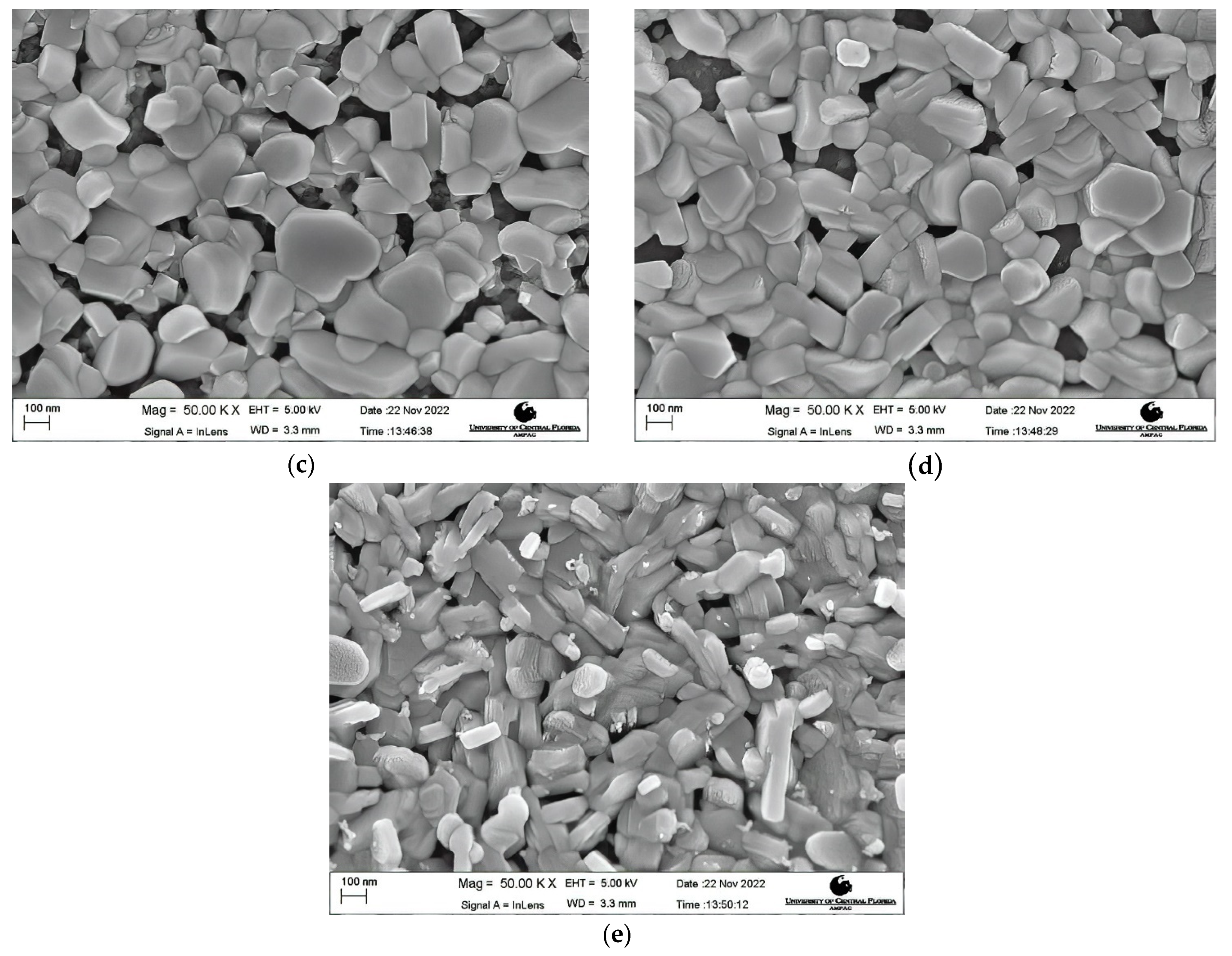
| Annealing temperatures | 600 °C, 650 °C, 750 °C, 800 °C, 900 °C |
| Annealing gas and flow rate | N2 at 300 sccm |
| Deposition Parameter | Specification |
|---|---|
| Sputtering gases | Ar |
| Base pressure | 1 × 10⁻⁵ Torr |
| Deposition pressure | 10 mTorr |
| RF power | 100 W |
| Substrate temperature | Room Temperature |
| Gas flow | 10 sccm |
| Thickness | 400 nm |
| Annealing Temperature (°C) | Phases Identified |
|---|---|
| 500 | - |
| 600 | Cr + CuO + CuCr2O4 |
| 650 | CuCrO2 (delafossite) |
| 750 | Cr + CuCrO2 |
| 800 | CuCrO2 + Cr2O3 |
| 900 | CuCrO2 + Cr2O3 |
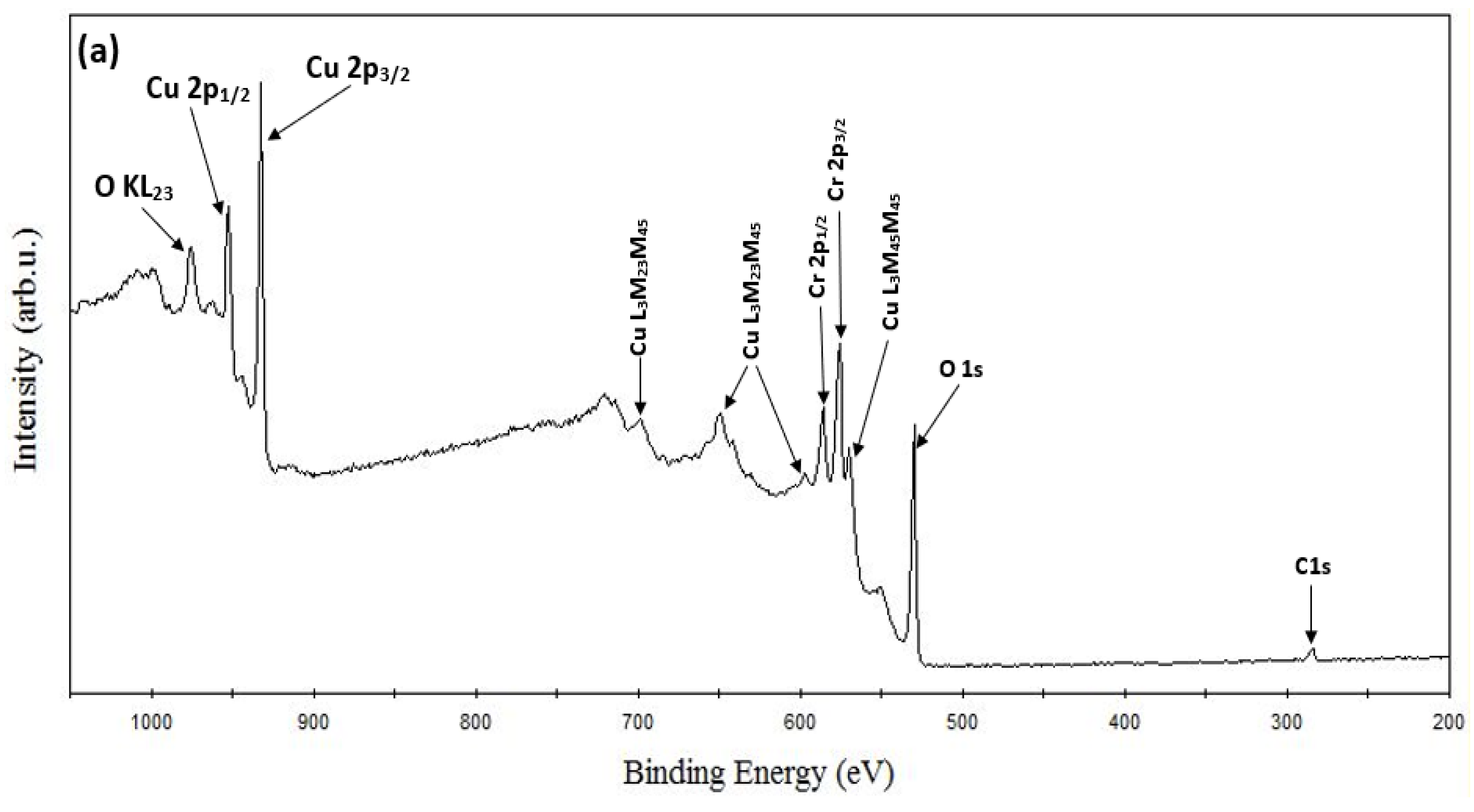
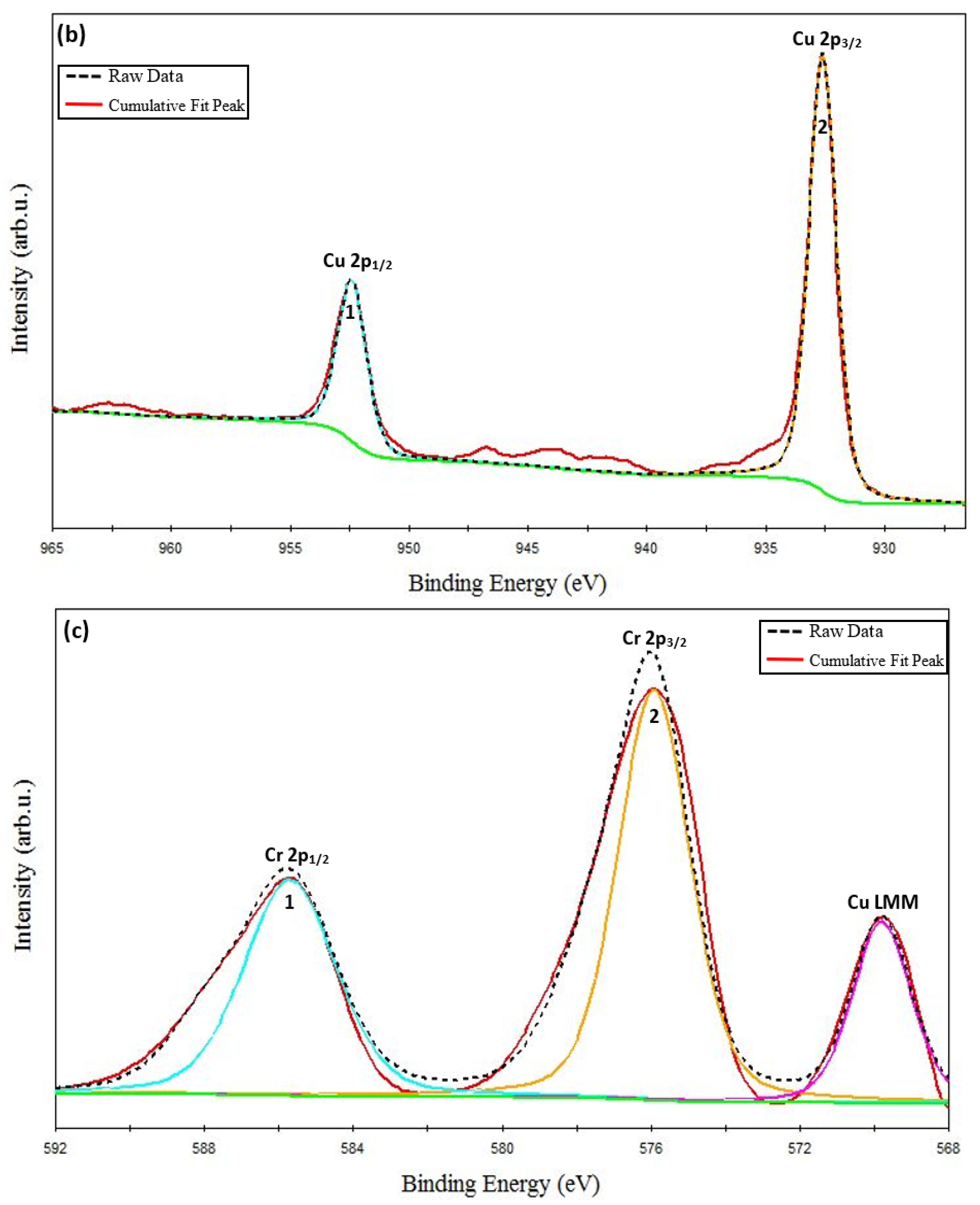
| Material | Peak | Oxidation State | Binding Energy (eV) | Satellite Peak (eV) | FWHM (eV) |
|---|---|---|---|---|---|
| CuCrO2 | Cu 2p3/2 | Cu1+ | 932.27 eV | - | 3.52 eV |
| Cu 2p1/2 | Cu1+ | 952.40 eV | - | 1.56 eV | |
| Cr 2p3/2 | Cr3+ | 576.16 eV | - | 4.45 eV | |
| Cr 2p1/2 | Cr3+ | 586.00 eV | - | 3.43 eV |
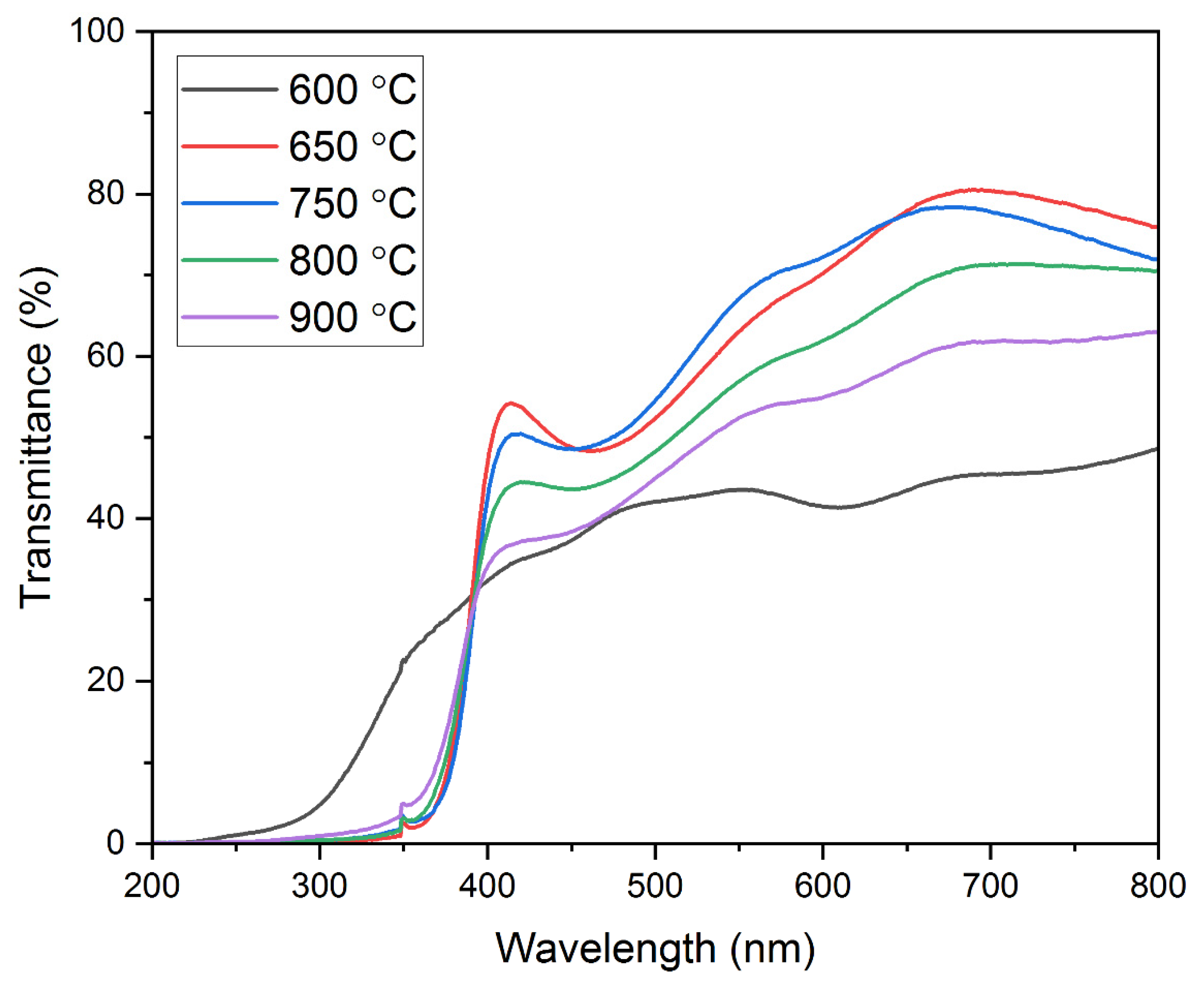
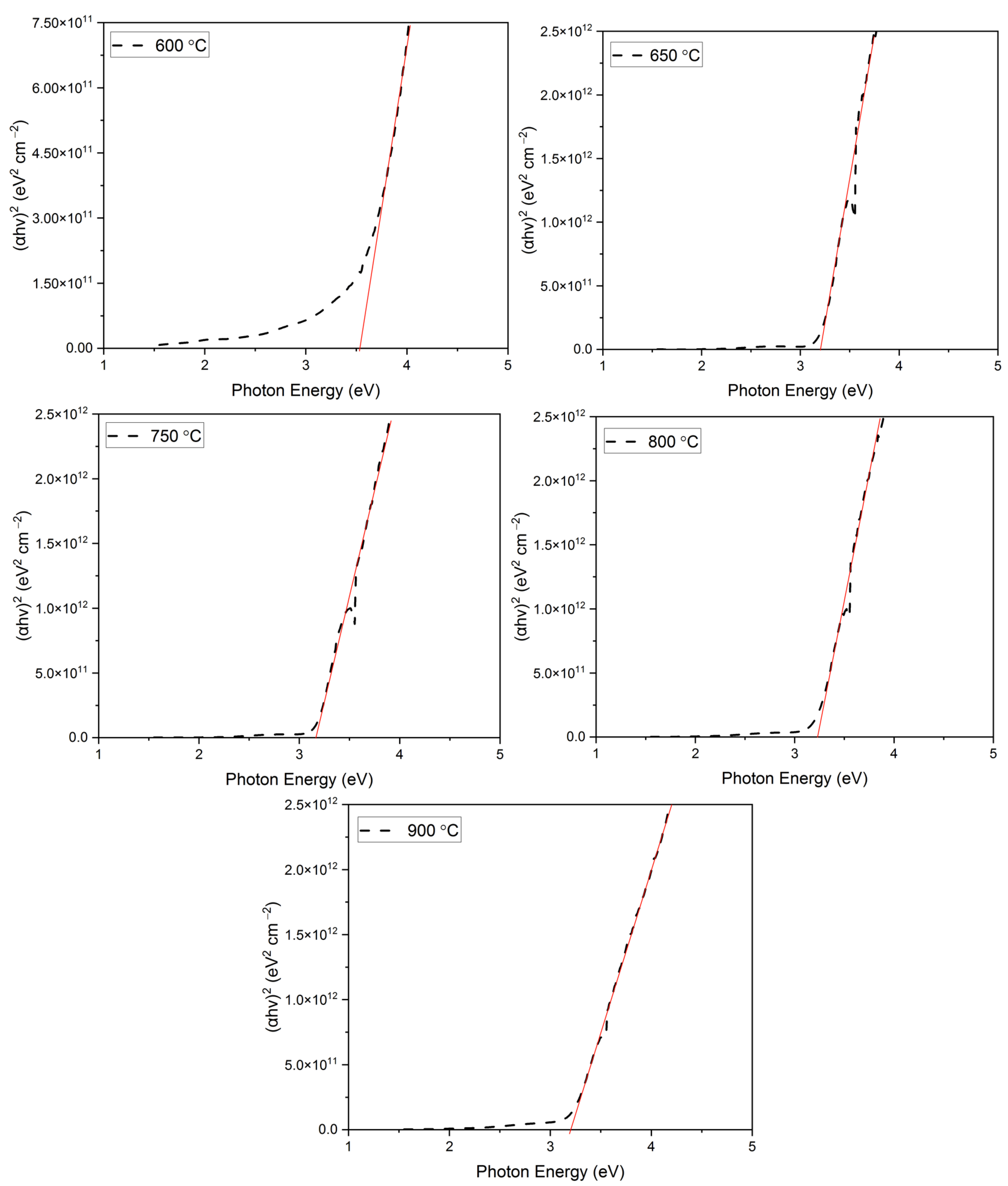
| Annealing Temperature (°C) | Bandgap (eV) |
|---|---|
| 600 | 3.52 |
| 650 | 3.21 |
| 750 | 3.20 |
| 800 | 3.18 |
| 900 | 3.16 |
Disclaimer/Publisher’s Note: The statements, opinions and data contained in all publications are solely those of the individual author(s) and contributor(s) and not of MDPI and/or the editor(s). MDPI and/or the editor(s) disclaim responsibility for any injury to people or property resulting from any ideas, methods, instructions or products referred to in the content. |
© 2023 by the authors. Licensee MDPI, Basel, Switzerland. This article is an open access article distributed under the terms and conditions of the Creative Commons Attribution (CC BY) license (https://creativecommons.org/licenses/by/4.0/).
Share and Cite
Sundaresh, S.; Bharath, A.H.; Sundaram, K.B. Effect of Annealing Temperature on Radio Frequency Sputtered p-Type Delafossite Copper Chromium Oxide (CuCrO2) Thin Films and Investigation of Diode Characteristics Forming Transparent pn-Heterojunction. Coatings 2023, 13, 263. https://doi.org/10.3390/coatings13020263
Sundaresh S, Bharath AH, Sundaram KB. Effect of Annealing Temperature on Radio Frequency Sputtered p-Type Delafossite Copper Chromium Oxide (CuCrO2) Thin Films and Investigation of Diode Characteristics Forming Transparent pn-Heterojunction. Coatings. 2023; 13(2):263. https://doi.org/10.3390/coatings13020263
Chicago/Turabian StyleSundaresh, Sreeram, Akash Hari Bharath, and Kalpathy B. Sundaram. 2023. "Effect of Annealing Temperature on Radio Frequency Sputtered p-Type Delafossite Copper Chromium Oxide (CuCrO2) Thin Films and Investigation of Diode Characteristics Forming Transparent pn-Heterojunction" Coatings 13, no. 2: 263. https://doi.org/10.3390/coatings13020263
APA StyleSundaresh, S., Bharath, A. H., & Sundaram, K. B. (2023). Effect of Annealing Temperature on Radio Frequency Sputtered p-Type Delafossite Copper Chromium Oxide (CuCrO2) Thin Films and Investigation of Diode Characteristics Forming Transparent pn-Heterojunction. Coatings, 13(2), 263. https://doi.org/10.3390/coatings13020263