Compact Dual-Band Rectenna Based on Dual-Mode Metal-Rimmed Antenna †
by
 , ,
, ,
Ha Vu Ngoc Anh
1,2,3 ,
,
Nguyen Minh Thien
3,4, 
Le Huy Trinh
1,2,3,* ,
,
Truong Nguyen Vu
5 and
Fabien Ferrero
6 1
Graduate University of Science and Technology, Vietnam Academy of Science and Technology, Hanoi 113000, Vietnam
2
Faculty of Computer Engineering, University of Information Technology, Ho Chi Minh City 721400, Vietnam
3
Vietnam National University, Ho Chi Minh City 721400, Vietnam
4
School of Electrical Engineering, International University, Ho Chi Minh City 721400, Vietnam
5
Institute of Applied Mechanics and Informatics, Vietnam Academy of Science and Technology, Hanoi 113000, Vietnam
6
LEAT, CNRS, Cremant, University of Nice—Sophia Antipolis, 06000 Nice, France
*
Author to whom correspondence should be addressed.
†
This manuscript is extension version of the conference paper: Trinh, L.H.; Vu Ngoc Anh, H.; Trinh, V.H.; Duy Phan, D.; Thi Khanh, H.N.; Ferrero, F. Design of a Dual-band Rectenna for Small IoT Terminal. In Proceedings of the 2019 International Symposium on Electrical and Electronics Engineering (ISEE), Ho Chi Minh, Vietnam, 10–12 October 2019; pp. 150–154, doi:10.1109/ISEE2.2019.8920853.
Electronics 2020, 9(9), 1532; https://doi.org/10.3390/electronics9091532
Submission received: 17 August 2020
/
Revised: 10 September 2020
/
Accepted: 15 September 2020
/
Published: 18 September 2020
(This article belongs to the Special Issue Design and Measurement of Integrated Antenna)
Abstract
:This paper proposes the design of a dual-band integrated rectenna. The rectenna has compact size of 0.4 × 0.3 × 0.25 cm and operates at 925 MHz and 2450 MHz bands. In general, the rectenna consists of two main parts, the metal-rimmed dual-band antenna used for harvesting the radio frequency (RF) signals from the environment and the rectifier circuit to convert these receiving powers to the direct current (DC). Because of the dual resonant structure of the antenna, the rectifier circuit can be optimized in terms of size and the frequency bandwidth, while the conversion efficiencies are always obtained 60% at the RF input power −2.5 dBm and −1 dBm for the lower band and the higher band, respectively. Measured results show that the metal-rimmed antenna exhibits −10 dB reflection coefficient in both desired frequency bands. Moreover, the antenna achieves 47% and 89% of total efficiency respectively at 925 MHz and 2450 MHz, which confirms that the proposed rectenna is well applicable in most of the miniaturized wireless sensor networks and IoT systems.
1. Introduction
The rise of wireless technology including IoT systems recently has achieved numerous essential accomplishments by bringing many benefits to important fields such as automation, health monitoring and industrial management. Moreover, wireless electronic devices have demonstrated their ability to support human communities and possibly slash environmental pollution. The basic principle of an IoT system is wirelessly connecting many kinds of devices so that they can communicate with each other. With the rapid growth of wireless modules working at the moment, many RF signals are emitted in environments such as WiFi, 2G, 3G, LTE, etc. Thanks to the ability to harvest these available RF signals and convert to DC power to use as the source of electronic devices [1], rectenna design has gained much attention in the development of wireless power transfer systems (WPT) [2]. The important feature of rectenna is the RF-to-DC conversion efficiency that needs to be optimized by using different structures or components. Hence, the main objective is to ensure a maximum DC power that is delivered to the load.
Recently, a variety of rectenna designs have been developed for many WPT applications. In [3], a differentially feeding microstrip patch antenna that connects with a differentially driven rectifier is presented. The proposed design obtains 73.9% of the maximum power conversion efficiency (PCE) at 207 W/cm input power density. In another paper [4], the ground plane of the antenna is printed with a triangular slot to keep only the fundamental harmonics. As reported in the result, the peak conversion efficiency reaches 75.043% at 20 dBm input power. These previous papers have shown high-efficiency rectenna designs. However, the single frequency band operation will limit their applications.
On the contrary, multi-band rectenna design certainly harvests more power sources [5,6,7,8,9,10,11,12]. In [5], the printed monopole antenna is miniaturized by two meander-lines, which operates at 900 MHz and 1800 MHz. The rectifier uses a dual-stub matching network to match the receiving antenna and the rectifier at two frequency bands. The maximum PCE achieves 72% at 900 MHz and 69% at 1800 MHz. However, in measurement, the antenna matching is not good enough and the physical profile of rectenna is quite high, which limit its applications. In [6], the authors investigate a microstrip antenna that differentially driven to work at dual frequency band of 2400 MHz and 5500 MHz. In both bands, the highest efficiency is measured about 90%. However, the rectifier efficiencies reach 35% at the lower band and 8% at the higher band. In another paper [7], the rectifier circuit is stacked with a dual-band patch antenna that has a specific matching network. By combining a /4 couple line and an open stub, a dual-band matching network is designed. The proposal achieves efficiencies of 56.3% at 2460 MHz and 37.8% at 5440 MHz. The rectifier requires high input power to achieve higher efficiency and voltage, which will reduce sensitivity and limit applications for low input power.
A dual-band monopole antenna is composed of two radiating arms for two frequency bands [8]. The longer arm is designed for GSM900 band radiation, while the shorter arm is for GSM1800 band. The rectifier circuit that uses a dual-band matching network is composed of multiple sections with several transmission lines and stubs. The first section is a shorted circuit stub that influences on the higher band matching. And then, the second section is open stubs that using for tuning the lower band matching. The peak PCE reaches 64% for the low-frequency band and 52% for the high-frequency band. In [9], an enhanced-gain antenna is integrated with the rectifying circuit for increasing the rectenna capability for scavenging. A four-section matching network is employed for the matching between the antenna and the rectifier. The rectenna gives 63% and 69% PCE at 1.95 GHz and 2.5 GHz, respectively.
A circular stub is used as the radiating element of the antenna [10]. Moreover, four symmetrical notches etched at the corner of the circular slot of the ground plane improve the overall antenna performance. The rectifying circuit employs a symmetrical matching network in addition to the symmetrical rectifier, thereby facilitating the suppression of the odd order harmonics. The symmetrical two-port rectifier circuit is then further combined using a microstrip line-based T-junction. The peak efficiency is obtained 70% at 1.8 GHz and 68% at 2.45 GHz. Another idea is reported in [11] that provides a miniature rectenna using the lumped component instead of the microstrip line. According to simulations results, the maximum PCE of the rectifier reaches 72% at 915 MHz and 67% at 2400 MHz. However, the rectifier requires a high input power level to achieve higher DC output voltage, which will limit applications for low input power. In [12], a maximum DC voltage obtains 1.8 V with the rectenna integrated with an array antenna. Nonetheless, the rectenna dimension is too large due to using a 7-stage Dickson multiplier that requires more diodes. Thus, this proposal will make it high cost and not appropriate for small size applications.
This paper is an extension of work originally presented in the 2019 International Symposium on Electrical and Electronics Engineering (ISEE 2019) [13]. The objective is to shows a rectenna operating at two ISM frequency bands 925 MHz and 2450 MHz in a compact size. The proposed design consists of a rectifier element printed on a 40 × 30 × 2.5 mm printed circuit board (PCB) combining with a dual-band rimmed antenna etched around the board. The rectenna design details are described in Section 2 and followed by the simulation results. Section 3 covers experimental results and some discussions to validate the proposed rectenna performance. Finally, the conclusion of the paper is given in Section 4.
2. Rectenna Structure and Simulation
2.1. Antenna Design
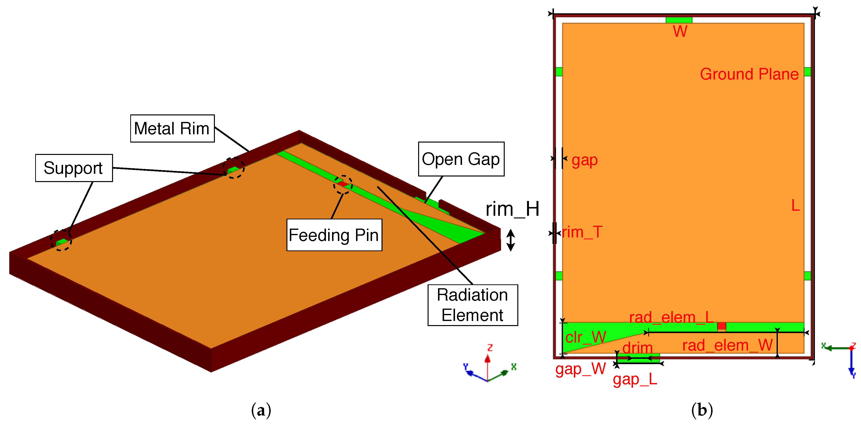
The proposed antenna is designed with the metal-rimmed structure as shown in Figure 1. The substrate is FR-4 with thickness of 0.8 mm, = 4.4 and tan = 0.02. Thanks to some parametric studies, the antenna parameters are optimized and indicated in Table 1. The proposed antenna consists of three main parts: the driven radiating element, the metal rim, and the ground plane associated with a supporting structure that aimed to fix the metal rim around the board. The radiating element is a metal trace with a trapezoidal shape. First, this trapezoidal patch is optimized to resonate and widen the matching bandwidth centered on 2400 MHz. Secondly, the metal rim allows capacitive coupling with the trapezoidal shape, therefore it produces another resonance at 925 MHz. It is observed that the input impedance of the antenna at 925 MHz band is significantly depended on the parameters of the open gap.
2.2. Rectifier Design
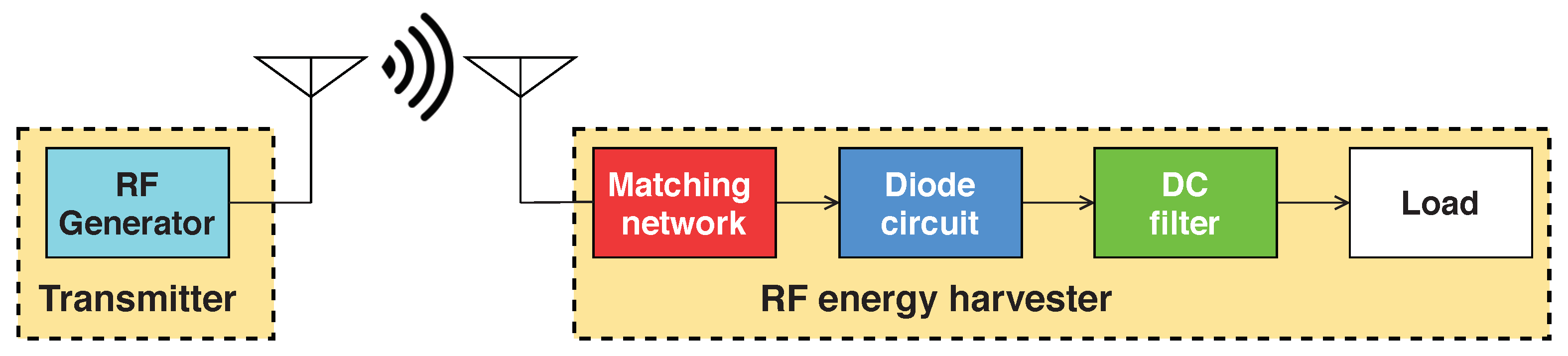
As shown in Figure 2, the rectifier circuit plays an important role in the WPT system. It includes three main elements: a matching network, a diode circuit, and a DC filter. The impedance matching network, first, is used as avoiding return loss and maximizing the power fed into the diode circuit. Secondly, thanks to the diodes, the rectifying circuit can rectify the RF signals that is obtained by the antenna. Finally, the unwanted high-order harmonics generated during the nonlinear rectification process can be suppressed with the help of the DC filter.
In this paper, Schottky diodes are used in the half-wave voltage doubler configuration (Figure 3) owing to their properties of minimal junction capacitance and the small forward-biased voltage. During the negative half cycle of the sinusoidal input waveform, diode D1 is forward biased and conducts charging up the pump capacitor, C1 to the peak value of the input voltage. At the same time, diode D2 conducts via D1 charging up capacitor, C2. During the positive half cycle, diode D1 is reverse biased blocking the discharging of C1 while diode D2 is forward biased charging up capacitor C2. However, there is a voltage across capacitor C1 already equal to the peak input voltage, capacitor C2 charges to twice the peak voltage value of the input signal.
Several simulations have been performed to check the most efficient Schottky diode in the rectifier configuration. The Skyworks SMS7630 is put in comparison with Avago HSMS-286x and shown similar efficiencies. However, as described in paper [2], with smaller package size and reduced parasitic capacitance and induction, the SMS7630 diode is suggested over the other one. The simulation program with integrated circuit emphasis (SPICE) model of SMS7630 is provided in Figure 3.
Several methods are considered to maximize the performance of the rectifier circuit. Using lumped components (capacitor, inductor, etc.) is one of the most effective ways of designing thanks to their small package, which helps reduce the dimension prominently. However, some certain limitations are probably producing an unexpected result for the actual final prototype. First, the value of the lumped components is limited, and the quality of the circuit would be dependent on their reliability. Secondly, all capacitors and inductors are not ideal components with purely capacitance or inductance, as they have the equivalent resistance producing losses on them. Alternatively, the use of the microstrip line is another technique that could solve the limitations of the lumped components. Nevertheless, that could make the performance of the rectifier depends on the substrate’s material and the circuit dimension would be increased significantly. Ultimately, the proposed rectenna is designed to take advantage of both methods by combining the lumped components and microstrip lines.
By using the Keysight ADS software, the structure of rectifier circuit as Figure 4 is designed and simulated. This part is placed on the bottom layer of antenna ground plane, with the combining of 0603 SMD (surface mounted) components. Table 2 shows the parameters of each element in the rectifier circuit. The proposed structure begins with the matching network, and then the diode circuit rectifies the input signal. The DC filter and the output load resistor go after the rectifying network. The PCE () indicated in Equation (1) is the ratio between DC power at the output and the received RF power:
where is output DC power, is input RF power, is output DC voltage and R is output load resistance.
2.3. Simulation Result
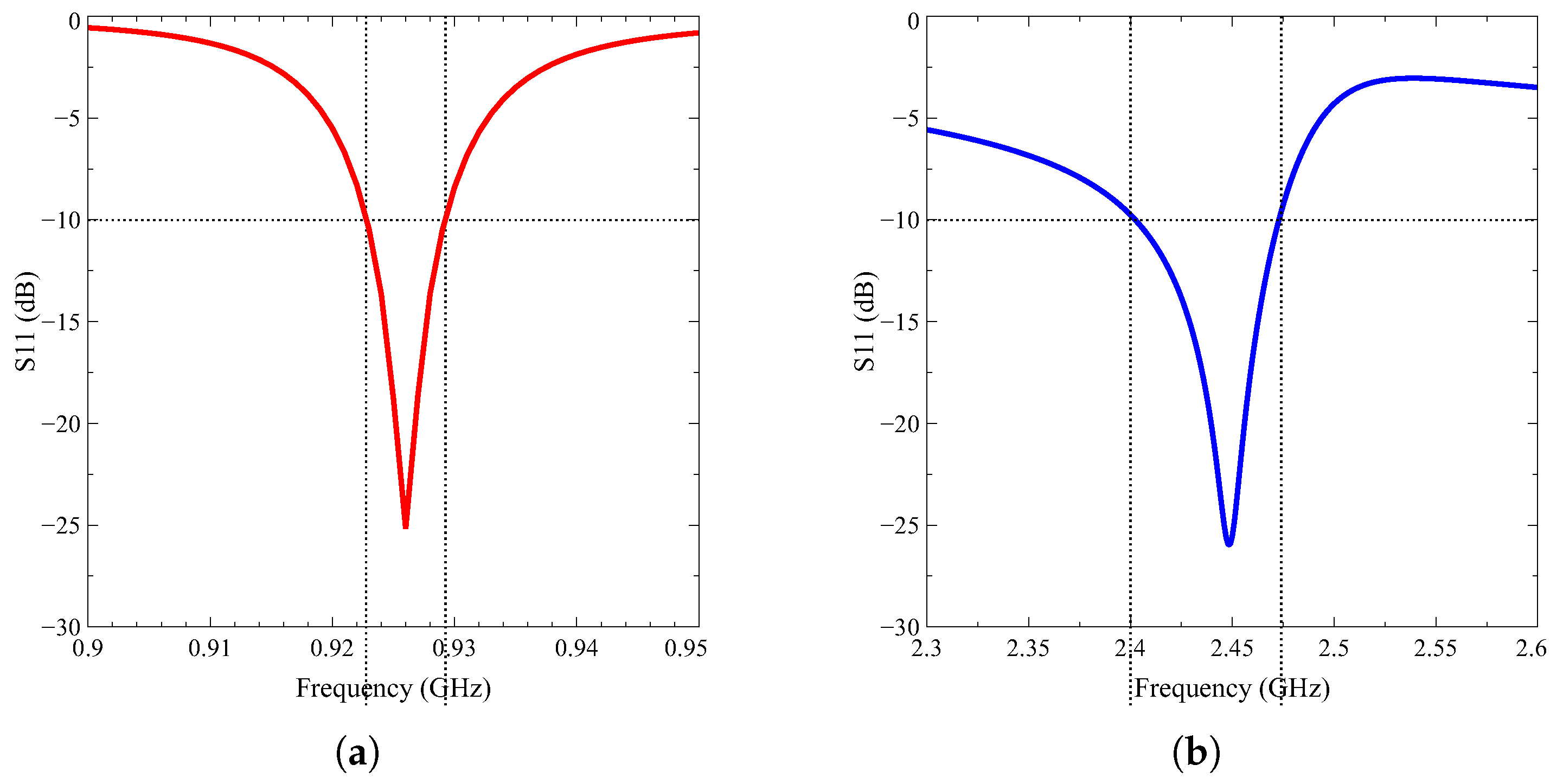
Figure 5 shows the simulated reflection coefficient of the proposed antenna at two frequency bands. The antenna demonstrates outstanding performance with −10 dB reflection coefficients from 922 MHz to 929 MHz and 2400 MHz to 2480 MHz.
The current distribution on the antenna at low- and high-frequency band is presented in Figure 6. At low-frequency band, the current density is mostly distributed on the metal rim and the edge of the ground plane. These results suggest that the dimension of metal rim and the distance from this part to the PCB have a huge impact on the resonance at the 925 MHz band. On the other hand, at the high-frequency band, the current concentrates on the microstrip trapezoid shape. It shows that the radiation element directly influences the antenna resonance at 2450 MHz band.
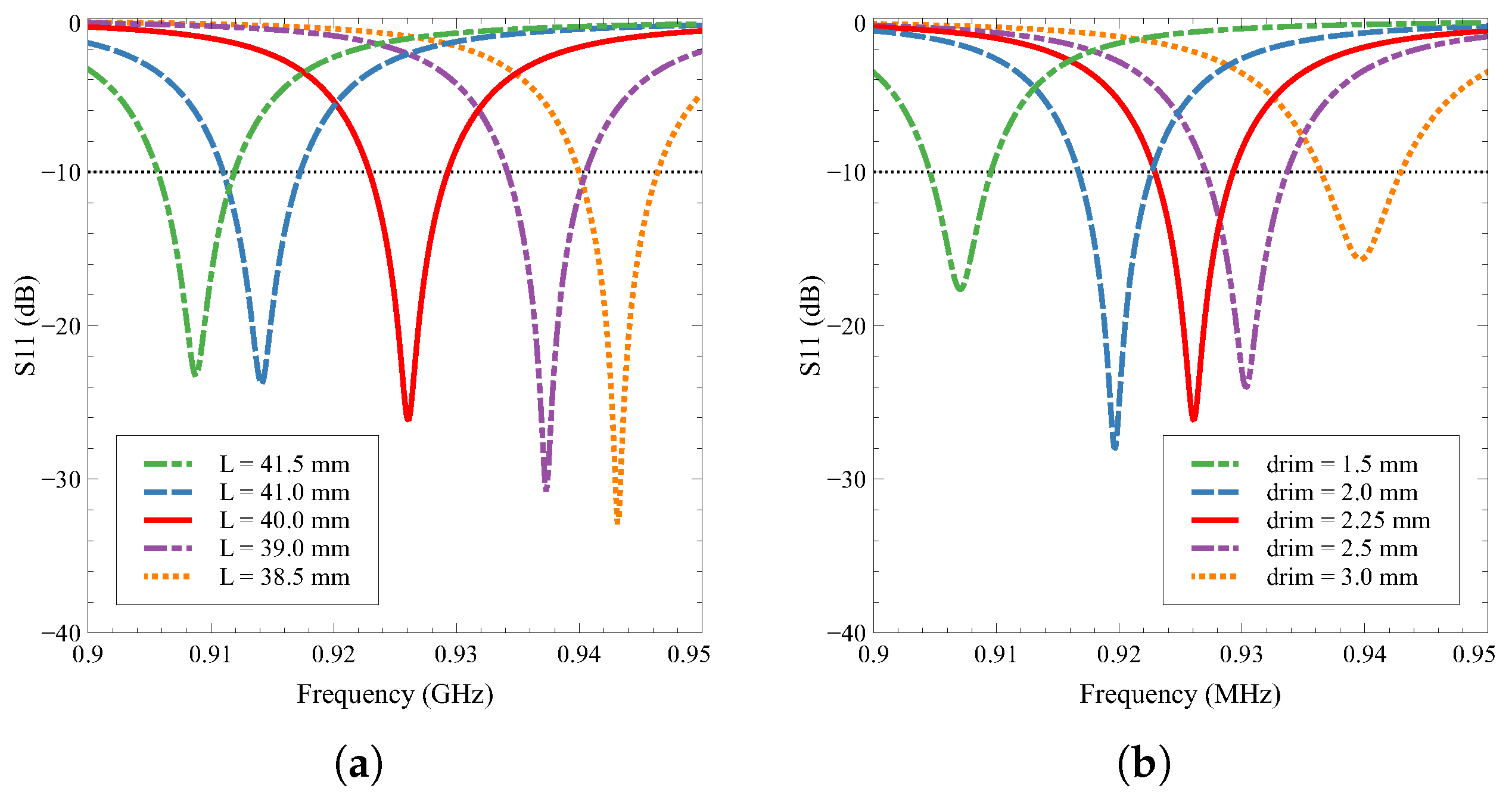
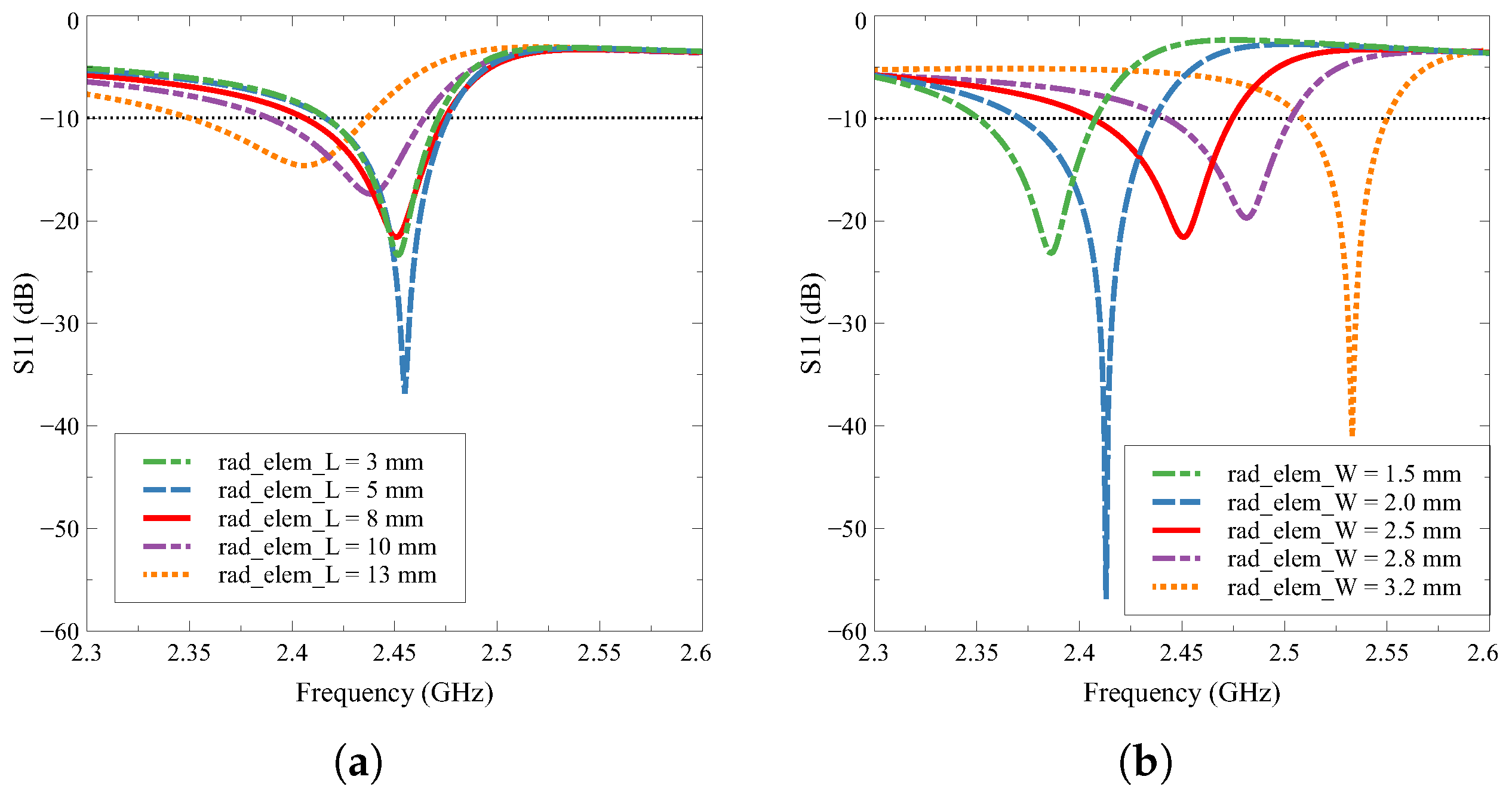
To be better understand resonance mechanism of the of the antenna, some parametric simulations are conducted on the gap (drim), the length of metal rim (L) and the shape of the radiation element’s structure (rad_elem_L, rad_elem_W). As indicated in Figure 7, the open gap and the length of the metal rim is turned that leads to the change of coupling between the feeding element and the metal rim.
Consequently, the resonance frequency is shifted, and the reflection coefficient is varied. On the other hand, Figure 8 presents resonances at the high-frequency band in different values of the gap width and rim length. Moreover, the simulated results indicate that resonant frequency shifts lower as the length of the shorter base of the trapezoid patch (rad_elem_L) increases. Also, when the width of the trapezoid (rad_elem_W) is changed, the resonant frequency is shifted as presented.
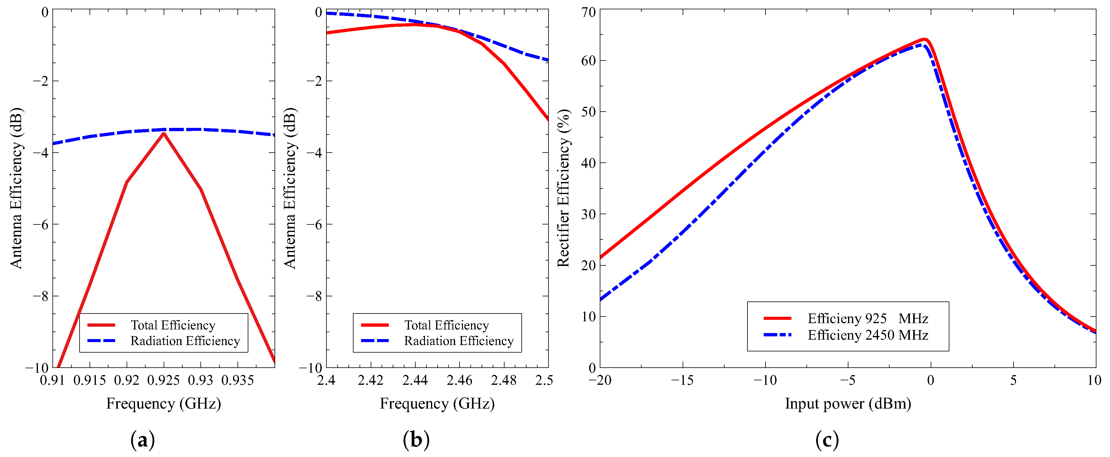
Finally, the antenna efficiency () is a ratio of the power radiated by the antenna () to the power supplied or (accepted) (). The higher efficiency, the more power radiated by the antenna. The lower efficiency, contrarily, the more power reflected to the power supplied owing to the mismatch.
The radiation efficiency is determined by the antenna loss but does not include the antenna impedance mismatch. The distinguishable term that includes also the power lost (or mismatch loss) is called the total efficiency (). It can be defined as the ratio of the antenna radiated power () relative to the power supplied to the antenna (), and the following equation expresses as:
where is the reflection coefficient, which is a complex quantity. The radiation efficiency would be the same as the total antenna efficiency if there was no loss due to impedance mismatch.
The maximum total efficiencies, as shown in Figure 9, are −3.3 dB, equivalent to 47% for the lower frequency band and −0.5 dB, equivalent to 89% for the higher frequency band, respectively. In Figure 9c, the simulation performance of the proposed rectifier at 925 MHz and 2450 MHz is reported. The rectifier obtains the PCE of 63% at 2450 MHz with an input power of −0.5 dBm. On the other hand, at the input power of −0.5 dBm, the PCE achieves 64% when the rectifier operates at 925 MHz. Additionally, the terminated output load resistor is optimized at R = 4000 to achieve the peak PCE. Over a broad range of input power from −10.8 dBm to 2.1 dBm and −12.8 dBm to 2.6 dBm at 2450 MHz and 925 MHz, respectively, the PCE is above 40%.
3. Experimental and Discussion
The antenna and the rectifier are measured separately to show the performance of each part. The proposed antenna PCB has been fabricated on the FR4-Epoxy substrate. The rim is formed by using a metal sheet with a thickness of 0.3 mm. This part is glued around PCB at six support points on the board. Then, the antenna port is connected with the inner conductor of RG402 coaxial cable, and the antenna ground plane is soldered with the outer conductor as shown in Figure 10b. The rectifier, on the other hand, is placed on the back of the antenna shown in Figure 10a. The antenna radiation measurement is performed in the anechoic chamber in MMIC Laboratory—HCM International University. The antenna radiation pattern is measured by Roll-over-Azimuth scanner system. This near-field measurement system is the best for measuring medium and low gain antenna. As indicated in Figure 10c, the rectenna is attached on the mount where the metal-rimmed antenna is placed normal to the direction toward the measurement probe.
3.1. Antenna Measurement
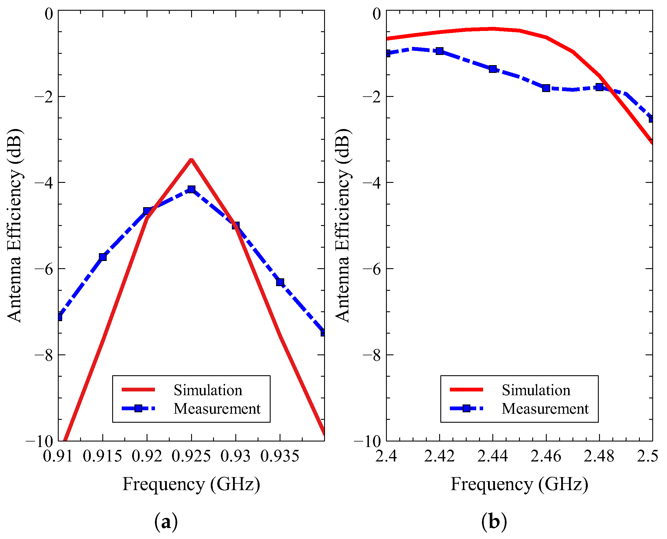
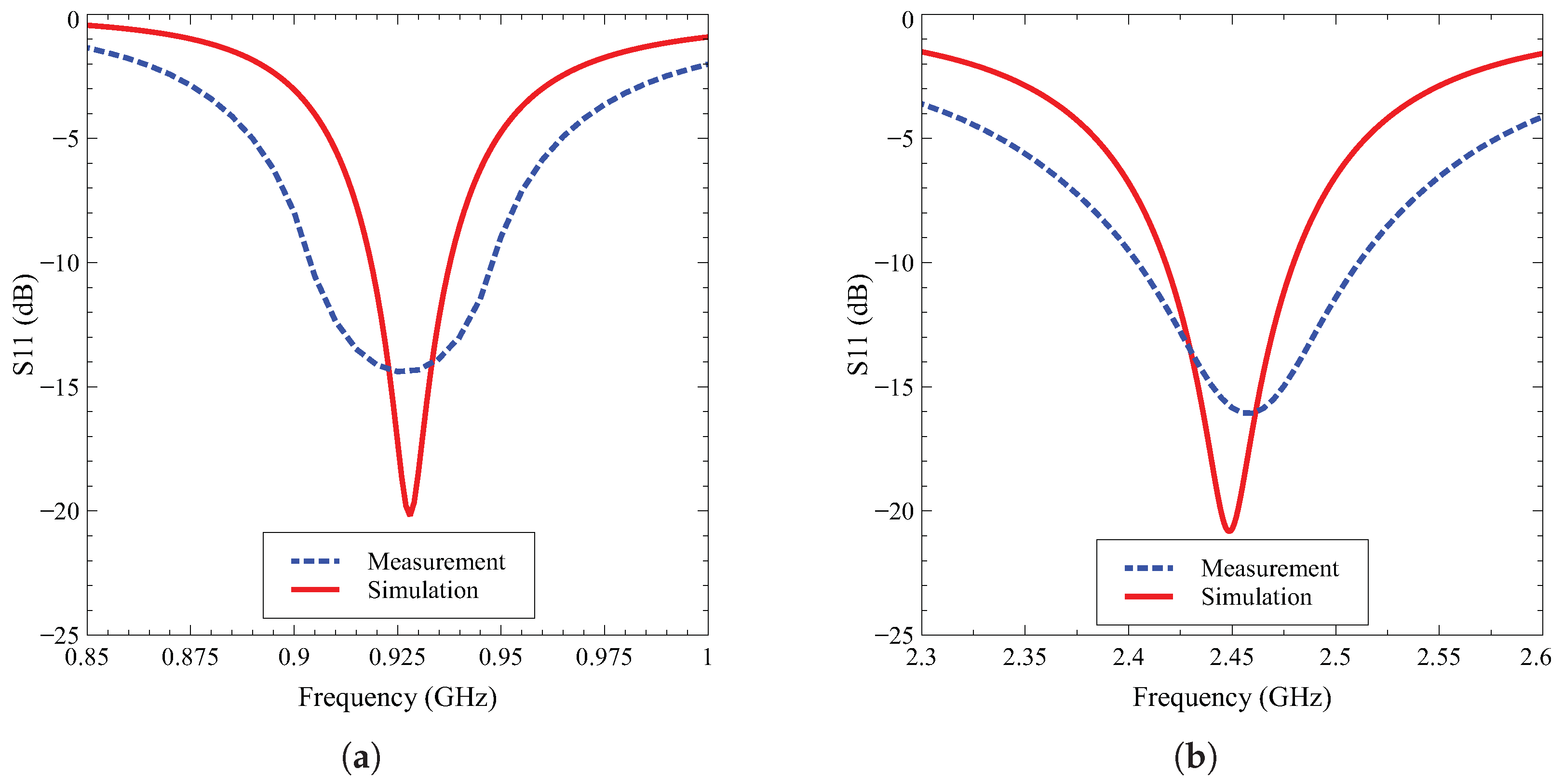
Figure 11 presents the comparison between the simulated and measured result of the reflection coefficient. At the low band, the antenna performs a good measurement result that is closely similar to simulation. On the contrary, there is a slight shift between the simulation and measurement results when the antenna operates at the high-frequency band. However, the shift is acceptable.
In terms of the antenna efficiency, the maximum efficiency reaches −4.1 dB for the low band and above −3 dB for the high band. The measured and simulated efficiency result in Figure 12 is different due to the change from the reflection coefficient of the antenna as indicated in Figure 11.
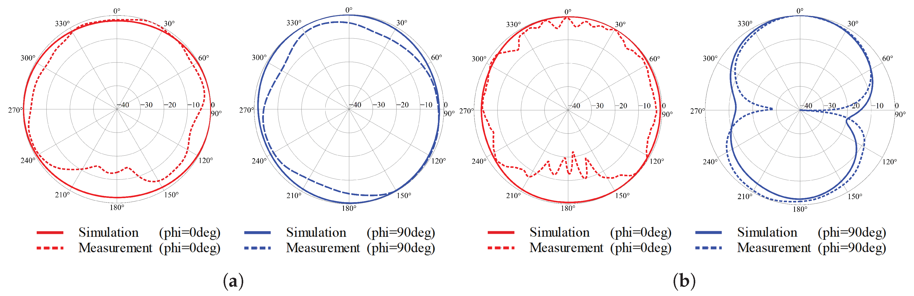
Figure 13 presents the measured normalized radiation pattern at the two planes = 90 and = 0 at 925 MHz and 2450 MHz. At low-frequency band, the proposed antenna shows a quasi-isotropic pattern that radio power radiates equally in all direction. At high-frequency band, on the other hand, the radio power is radiated as the omni-directional pattern. However, there are some mismatches between simulation and measurement shown in the pattern. It can be explained due to inevitable fabrication errors and imperfect measurement setup.
3.2. Rectifier Measurement
Figure 14 presents the comparison between the simulated and measured result of the reflection coefficient of the rectifier. These results are slightly different at low and high-frequency band. It could be explained that because there are some losses of the material of the substrate and values of the lumped components. However, the rectifier performs a good measurement results that are less than −10 dB of the return loss for dual-band.
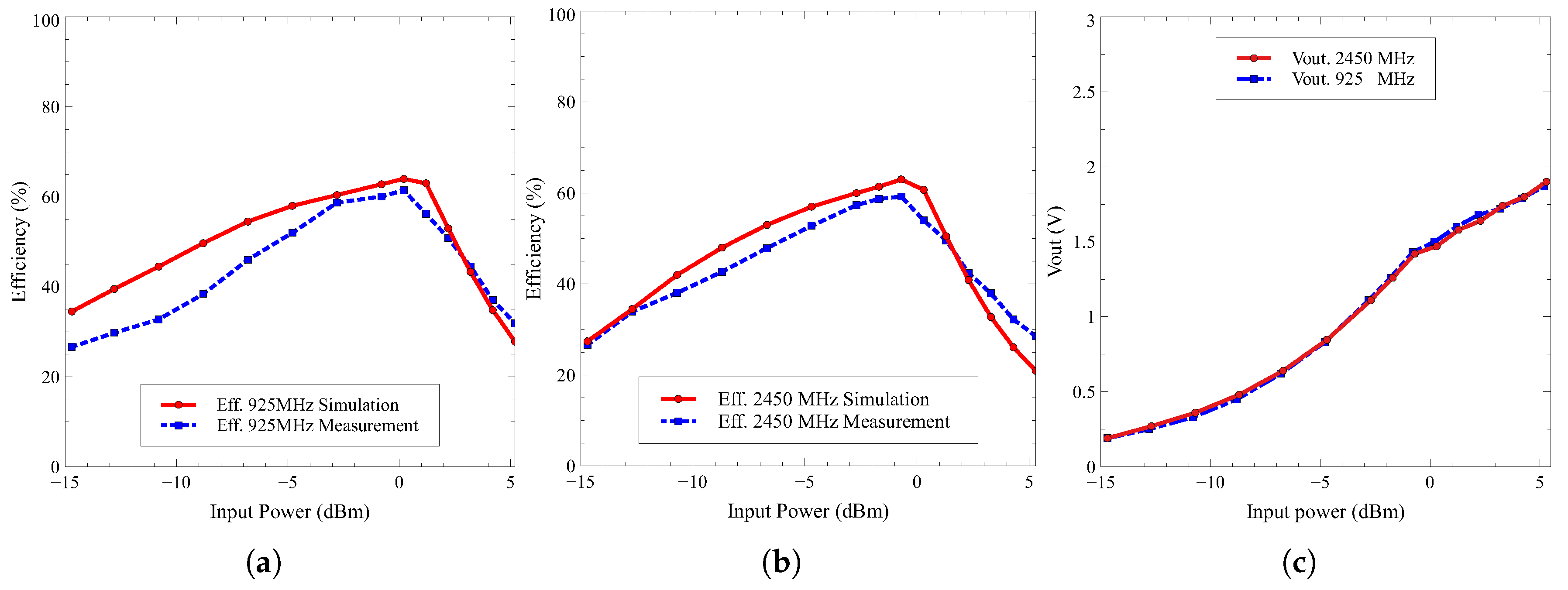
With optimal output load resistor R = 4000 , efficiency and output voltage at two frequency band of the rectifier can be achieved at the highest level as indicated in Figure 15. Figure 15a,b presents the efficiency at 925 MHz and 2450 MHz. It can be observed that the rectifier achieves 61.4% at input power −0.8 dBm and 59.2% at −0.7 dBm for low and high-frequency band, respectively. The simulated and measured results are slightly different that can be explained due to the mismatch and the loss of input power during measurement process. For the measurement value of DC output voltage, the rectifier reaches 1.42 V at −0.7 dBm for the high-frequency band and 1.43 V at −0.8 dBm for the low-frequency band. As shown in Figure 15c, it is identical when comparing the output voltage at 925 MHz to 2450 MHz.
4. Conclusions
A design of rectenna with metal-rimmed antenna is proposed for dual-band operation. Both simulated and measured results agree that the proposed rectifier reaches approximately 60% at both desire frequency bands. Additionally, the proposed antenna structure provides not only less than −10 dB of the return loss for dual-band but also the total efficiency above 47% in 925 MHz band and 89% in 2450 MHz band. The pinnacle of this proposed rectenna structure is its compact size while high efficiency is maintained. A Figure of Merit (F.o.M.) equation was calculated using Equation (4) is proposed to evaluate the rectenna performance. To obtain high F.o.M., the rectenna not only should be operated in many bands and achieved high efficiency but also the dimension is optimized to have the smallest size. Table 3 shows the comparison of the proposed rectenna with some previous works. It indicates that the proposed has a better performance compared to some published works.
Author Contributions
Conceptualization, L.H.T.; Methodology, L.H.T. and H.V.N.A.; software, F.F. and N.M.T.; validation, L.H.T., T.N.V. and F.F.; formal analysis, F.F.; resources, F.F.; data curation, H.V.N.A. and N.M.T.; writing—original draft preparation, L.H.T. and H.V.N.A.; writing—review and editing, N.M.T. and F.F.; supervision, L.H.T. and F.F.; All authors have read and agreed to the published version of the manuscript.
Funding
This research is funded by Graduate University of Science and Technology under grant number GUST.STS.DT2017-TT01. The APC was funded by LEAT-CNRS UMR 7248.
Conflicts of Interest
The authors declare no conflict interest.
References
- Visser, H.J.; Vullers, R.J.M. RF Energy Harvesting and Transport for Wireless Sensor Network Applications: Principles and Requirements. Proc. IEEE 2013, 101, 1410–1423. [Google Scholar] [CrossRef]
- Valenta, C.R.; Durgin, G.D. Harvesting Wireless Power: Survey of Energy-Harvester Conversion Efficiency in Far-Field, Wireless Power Transfer Systems. IEEE Microw. Mag. 2014, 15, 108–120. [Google Scholar]
- Sun, H. An Enhanced Rectenna Using Differentially-Fed Rectifier for Wireless Power Transmission. IEEE Antennas Wirel. Propag. Lett. 2016, 15, 32–35. [Google Scholar] [CrossRef]
- Ahmed, S.; Zakaria, Z.; Husain, M.N.; Ibrahim, I.M.; Alhegazi, A. Efficient feeding geometries for rectenna design at 2.45 GHz. Electron. Lett. 2017, 53, 1585–1587. [Google Scholar] [CrossRef]
- Ho, D.; Kharrat, I.; Ngo, V.; Vuong, T.; Nguyen, Q.; Le, M. Dual-band rectenna for ambient RF energy harvesting at GSM 900 MHz and 1800 MHz. In Proceedings of the 2016 IEEE International Conference on Sustainable Energy Technologies (ICSET), Hanoi, Vietnam, 14–16 November 2016; pp. 306–310. [Google Scholar]
- Mattsson, M.; Kolitsidas, C.I.; Jonsson, B.L.G. Dual-Band Dual-Polarized Full-Wave Rectenna Based on Differential Field Sampling. IEEE Antennas Wirel. Propag. Lett. 2018, 17, 956–959. [Google Scholar] [CrossRef]
- Lin, D.; Yu, C.; Lin, C.; Lee, Y. Dual band rectenna with one rectifier. In Proceedings of the 2017 International Symposium on Electronics and Smart Devices (ISESD), Yogyakarta, Indonesia, 17–19 October 2017; pp. 268–272. [Google Scholar]
- Zeng, M.; Li, Z.; Andrenko, A.S.; Zeng, Y.; Tan, H.-Z. A Compact Dual-Band Rectenna for GSM900 and GSM1800 Energy Harvesting. Int. J. Antennas Propag. 2018, 2018, 4781465. [Google Scholar] [CrossRef] [Green Version]
- Aboualalaa, M.; Mansour, I.; Mansour, M.; Bedair, A.; Allam, A.; Abo-Zahhad, M.; Elsadek, H.; Yoshitomi, E.; Pokharel, R.K. Dual-band Rectenna Using Voltage Doubler Rectifier and Four-Section Matching Network. In Proceedings of the 2018 IEEE Wireless Power Transfer Conference (WPTC), Montreal, QC, Canada, 3–7 June 2018; pp. 1–4. [Google Scholar]
- Chandravanshi, S.; Akhtar, M.J. An efficient dual-band rectenna using symmetrical rectifying circuit and slotted monopole antenna array. Int. J. Microw. RF Comput.-Aided Eng. 2020, 30, e22117. [Google Scholar] [CrossRef]
- Almohaimeed, A.M.; Yagoub, M.E.E.; Lima, J.A.; Amaya, R.E. Dual-Band Harvester with Wide Range Input Power for WPT Applications. In Proceedings of the 2018 IEEE PELS Workshop on Emerging Technologies: Wireless Power Transfer (Wow), Montréal, QC, Canada, 3–7 June 2018; pp. 1–4. [Google Scholar]
- Adam, I.; Yasin, N.; Rahim, H.A.; Soh, P.J.; Abdulmalek, M. A compact dual-band rectenna for ambient RF energy harvesting. Microw. Opt. Technol. Lett. 2018, 60, 2740–2748. [Google Scholar] [CrossRef]
- Trinh, L.H.; Vu Ngoc Anh, H.; Trinh, V.H.; Duy Phan, D.; Thi Khanh, H.N.; Ferrero, F. Design of a Dual-band Rectenna for Small IoT Terminal. In Proceedings of the 2019 International Symposium on Electrical and Electronics Engineering (ISEE), Ho Chi Minh, Vietnam, 10–12 October 2019; pp. 150–154. [Google Scholar] [CrossRef]
Figure 1.
The structure of proposed antenna in (a) isometric view and (b) top view.

Figure 2.
Block structure of the RF energy harvester.

Figure 3.
Diode circuit and simulation program with integrated circuit emphasis (SPICE) model.
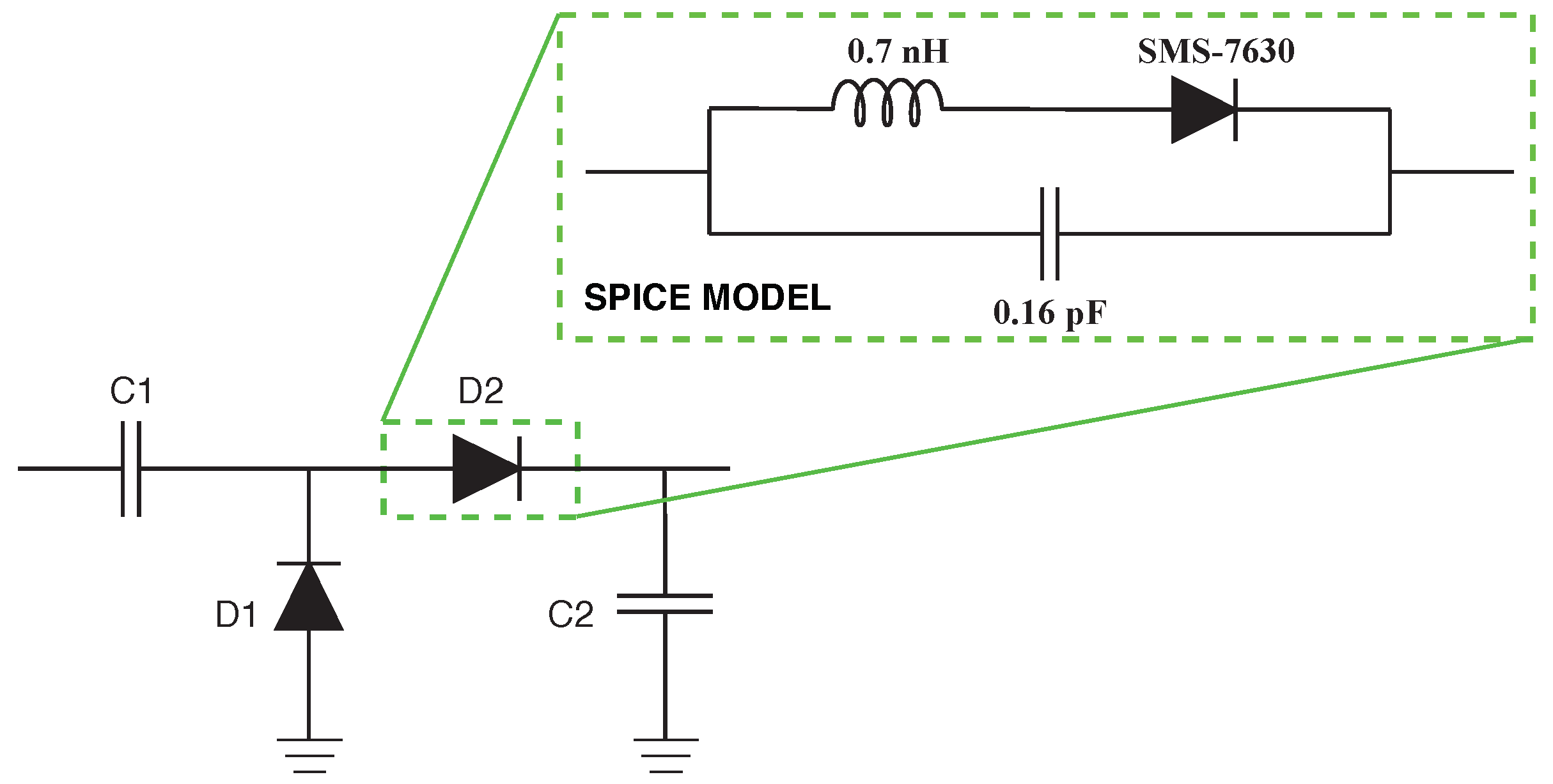
Figure 4.
Topology of the dual-band rectifier.
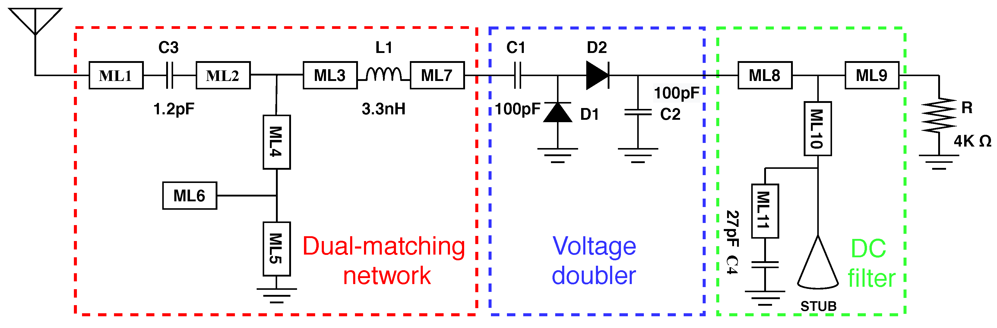
Figure 5.
Simulated reflection coefficient of the antenna at (a) low-frequency band and (b) high-frequency band.
Figure 5.
Simulated reflection coefficient of the antenna at (a) low-frequency band and (b) high-frequency band.

Figure 6.
Simulated surface current distribution of the antenna at (a) low-frequency band and at (b) high-frequency band.
Figure 6.
Simulated surface current distribution of the antenna at (a) low-frequency band and at (b) high-frequency band.
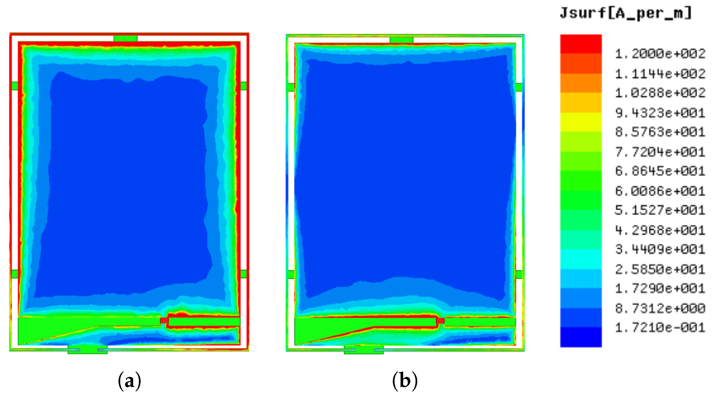
Figure 7.
Simulated reflection coefficient at low-frequency band with variations of (a) the length of metal rim (L) and (b) open gap (drim).
Figure 7.
Simulated reflection coefficient at low-frequency band with variations of (a) the length of metal rim (L) and (b) open gap (drim).

Figure 8.
Simulated reflection coefficient at high-frequency band with variations of (a) the length of the short side (rad_elem_L) and (b) the width of the trapezoid (rad_elem_W).
Figure 8.
Simulated reflection coefficient at high-frequency band with variations of (a) the length of the short side (rad_elem_L) and (b) the width of the trapezoid (rad_elem_W).

Figure 9.
Simulated results of rectenna. The antenna efficiency of (a) at low-frequency band and (b) at high-frequency band. (c) The efficiency of rectifier circuit.
Figure 9.
Simulated results of rectenna. The antenna efficiency of (a) at low-frequency band and (b) at high-frequency band. (c) The efficiency of rectifier circuit.

Figure 10.
Realization of (a) rectifier, (b) antenna and (c) measurement setup.
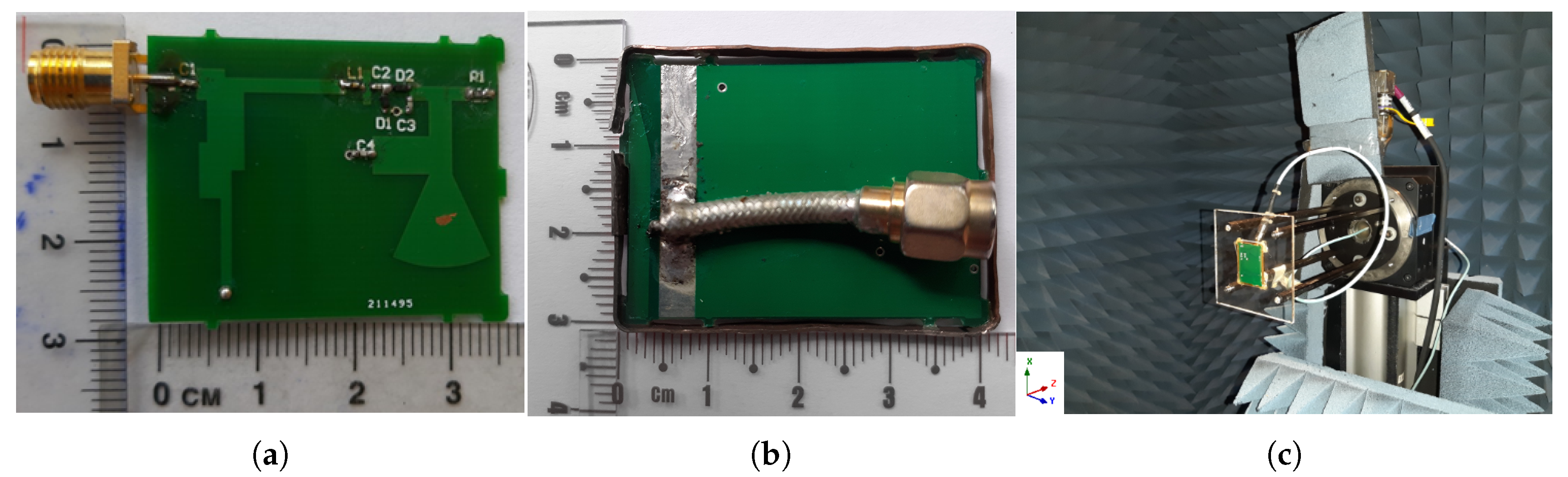
Figure 11.
Simulated and measured reflection coefficient of the antenna at (a) low-frequency band and (b) high-frequency band.
Figure 11.
Simulated and measured reflection coefficient of the antenna at (a) low-frequency band and (b) high-frequency band.
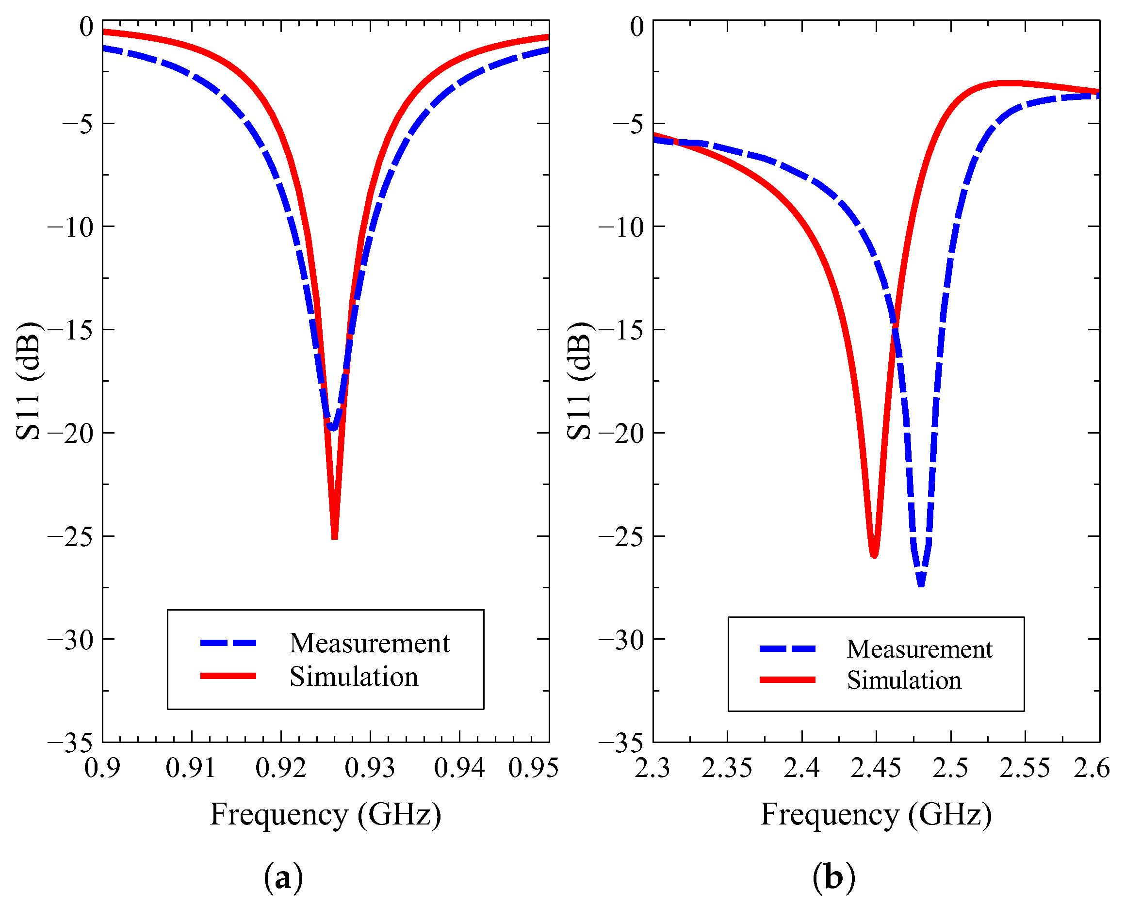
Figure 12.
Simulated and measured total efficiency of the antenna at (a) low-frequency band and (b) high-frequency band.
Figure 12.
Simulated and measured total efficiency of the antenna at (a) low-frequency band and (b) high-frequency band.

Figure 13.
Measured normalized radiation pattern of the antenna at (a) low-frequency band and (b) high-frequency band.
Figure 13.
Measured normalized radiation pattern of the antenna at (a) low-frequency band and (b) high-frequency band.

Figure 14.
Simulation and measurement reflection coefficient of the rectifier at (a) low-frequency band and (b) high-frequency band.
Figure 14.
Simulation and measurement reflection coefficient of the rectifier at (a) low-frequency band and (b) high-frequency band.

Figure 15.
Efficiency at (a) low-frequency band, (b) high-frequency band and (c) output voltage of the rectifier.
Figure 15.
Efficiency at (a) low-frequency band, (b) high-frequency band and (c) output voltage of the rectifier.


Table 1.
Antenna parameters.
| Parameter | Value (mm) | Parameter | Value (mm) |
|---|---|---|---|
| clr_W | 3.6 | gap_W | 1.1 |
| rad_elem_L | 18.2 | gap_L | 5.5 |
| rad_elem_W | 2.5 | gap | 0.8 |
| W | 30 | rim_H | 2.5 |
| L | 40 | rim_T | 0.3 |
| drim | 2.25 |
Table 2.
Rectifier circuit parameters.
| Value (mm) | Value (mm) | ||||
|---|---|---|---|---|---|
| Parameter | Width | Length | Parameter | Width | Length |
| ML1 | 1.5 | 1 | ML7 | 3.6 | 0.9 |
| ML2 | 3.2 | 1 | ML8 | 1.5 | 1 |
| ML3 | 1.5 | 10.4 | ML9 | 1.5 | 1 |
| ML4 | 3.7 | 4.2 | ML10 | 3.3 | 3.3 |
| ML5 | 1.1 | 9.5 | ML11 | 4.5 | 5.5 |
| ML6 | 5.5 | 0.8 | ML_STUB | 3.3 | 9.4 |
Table 3.
Comparison Between the Proposed Rectenna and Some Related References.
| Ref. | Bands (MHz) | Max. Conversion Eff. (%) | Electrical Size | F.o.M. |
|---|---|---|---|---|
| [3] | 2450 | 73.9 | 1.58 | |
| [4] | 2450 | 75 | 1.32 | |
| [5] | 900/1800 | 72/69 | 16.86 | |
| [6] | 2400/5500 | 36/8 | 0.627 | |
| [7] | 2450/5480 | 56.3/37.8 | 2.57 | |
| [8] | 880/1850 | 62/50 | 21.72 | |
| [10] | 1800/2450 | 70/68 | 1.78 | |
| This Work | 925/2450 | 64/63 | 111.02 | |
| * is the wavelength at the center frequency for the single band or at the lowest frequency for the multi-band. | ||||
© 2020 by the authors. Licensee MDPI, Basel, Switzerland. This article is an open access article distributed under the terms and conditions of the Creative Commons Attribution (CC BY) license (http://creativecommons.org/licenses/by/4.0/).
Share and Cite
MDPI and ACS Style
Vu Ngoc Anh, H.; Thien, N.M.; Trinh, L.H.; Nguyen Vu, T.; Ferrero, F. Compact Dual-Band Rectenna Based on Dual-Mode Metal-Rimmed Antenna. Electronics 2020, 9, 1532. https://doi.org/10.3390/electronics9091532
AMA Style
Vu Ngoc Anh H, Thien NM, Trinh LH, Nguyen Vu T, Ferrero F. Compact Dual-Band Rectenna Based on Dual-Mode Metal-Rimmed Antenna. Electronics. 2020; 9(9):1532. https://doi.org/10.3390/electronics9091532
Chicago/Turabian StyleVu Ngoc Anh, Ha, Nguyen Minh Thien, Le Huy Trinh, Truong Nguyen Vu, and Fabien Ferrero. 2020. "Compact Dual-Band Rectenna Based on Dual-Mode Metal-Rimmed Antenna" Electronics 9, no. 9: 1532. https://doi.org/10.3390/electronics9091532
Note that from the first issue of 2016, this journal uses article numbers instead of page numbers. See further details here.