Article

Comparative Study on Reliability and Advanced Numerical Analysis of BGA Subjected to Product-Level Drop Impact Test for Portable Electronics

1
Global Technology Center, Samsung Electronics Co., Ltd., Samsung-ro Yeongtong-gu Suwon-si, Gyeonggi-do 16677, Korea
2
Department of Mechanical Engineering, Chosun University, Gwangju 61452, Korea
*
Author to whom correspondence should be addressed.
Electronics 2020, 9(9), 1515; https://doi.org/10.3390/electronics9091515
Submission received: 5 August 2020 / Revised: 7 September 2020 / Accepted: 9 September 2020 / Published: 15 September 2020

Abstract

:
In this paper, drop reliability of various PBA (printed board assembly) mounting structures is investigated and compared. Then, we built SAC305 (Sn3.0Ag0.5Cu) interconnects for BGA (ball grid array) package failure model to evaluate the drop impact reliability of handheld devices. In order to simulate actual behavior of the solder joint under the drop impact load of handheld devices, we perform explicit full FEA (finite element analysis) modeling. However, this takes a lot of computing time because of the large aspect ratio of element size between solder joints and other structures such as PCB (printed circuit board) and electronic packages. Therefore, an effective way to represent solder interconnects for FEA is needed which would be relatively simpler yet detailed. Comparable board-level drop tests are conducted after equipping test vehicles with various fixtures considering PBA mounting structures, which make it possible to apply different loading conditions to BGA packages. The results show different drop impact life for solder interconnects depending on the mounting design of the PBA. Particularly, the solder interconnect of the component located at the middle of the PCB exhibits the shortest impact life where the highest tensile stress occurs. Also, the mounting design restraining PBA deflections shows better reliability under the drop impact loading. Sequentially, simulating with a PBA composed of the BGA package and the PCB is considered to assess the feasibility of the solder ball failure modeling when the drop impact load is applied. Especially, for the modeling of the solder balls, detailed solid model and simple beam model are compared regarding computational efficiency and numerical accuracy. We found that the simple beam model significantly shortens computational time from 110 h to less than an hour. Accordingly, the feasibility of the beam model for the solder balls is shown by correlating the stress level and the drop impact life obtained from the experiments.

1. Introduction

Because of the slim design, handheld devices are becoming more vulnerable in case of the drop. As electronic packages are also getting thinner, drop and vibration reliability concerns become increasingly more important [1,2,3,4,5]. Especially, interconnection structures of the IC (integrated circuit) packages are sensitive to drop impact conditions when PCB thickness is reduced. On the other hand, modern design tends to minimize the number of screws used to mount these slim PBA for reasons of cost-effectiveness of the assembly process. As shown in Figure 1, various structural designs exist using both screw fastening and hook locking for PBA mounting in portable electronics. Drop reliability and IC package lifetime should be assessed in the development stage of the mobile product. This requires a database of records of structural designs of the PBA mounting and effective FEA of the drop impact performance for IC packages. Accordingly, we have carried out a study to better understand the dynamic behavior of interconnections of the electronics package and the effect of the mounting design. Among various IC packages, we examined the BGA package because its popularity in mobile electronics. Drop reliability of various PBA assembly designs is compared in terms of characteristic life, and failure modeling and criterion for drop simulation are established for specific BGA packages.
First, board-level drop tests are conducted after equipping test vehicles with various fixtures considering PBA mounting structures, which make it possible to apply different impact loads to the BGA packages. The failure of BGA package under the drop impact condition mainly occurs around the solder balls at the outermost array, especially at the corner as reported by previous researchers [6,7,8]. In addition, the representative failure modes were found as a crack in the IMC (inter-metallic compound) layer of the solder joint and the PCB pad cratering under drop impact loading [9,10,11,12]. In this study, we consider three PBA mounting structures as boundary conditions with a variation in the amount of displacement that can be applied to the solder joints. Based on JEDEC (joint electron device engineering council) standard, the drop test is sequentially conducted and repeated until the electric connection of the BGA package is cut off by monitoring the resistance change (i.e., daisy-chain connection failure). The drop life for each boundary condition is obtained for the validation of the failure model.
Next, drop simulation of the BGA package is carried out. Although the solder ball is the smallest component in the PBA model it is the most essential one since the BGA package failure always happens around the solder interconnects. IC package modeling and simulation of the drop event is extensively discussed in the literature. Wu and Lan [13] used a numerical method to investigate the stress and strain of the solder joint during drop test and then, established a predictive fatigue life model for SAC105 and SAC1205N solder joint. Xu et al. [14] proposed a numerical method to investigate the plastic strain hardening effect of lead-free solder joints in PCB assembly subject to mechanical drop test. Zhu and Marcinkiewicz [15] introduced sub-modeling and explicit-implicit sequential modeling techniques to efficiently characterize the dynamic responses of CSP/BGA packages in different board designs. Tee et al. [16] and Tee et al. [17] established an impact life prediction modeling for various types of BGA and QFN (quad-flat no-leads) packages. However, there is still lack of numerical solutions to effectively reduce the computing time with maintaining accuracy of analysis for dynamic modeling. In this study, in order to represent the minute solder joint compared to the PCB, the sub-modeling technique is used by replacing solid elements with beam elements. In addition, the elasto-plastic property of the SAC305 characterized by Nguyen and Park [18] is applied to FEA modeling so that the solder joint accurately simulates actual stress–strain behavior under such a high strain rate of the impact loading.
As a failure criterion of the solder joint, the plastic strain of the solder joint or the peeling force/stress between the bulk solder and the IMC are used. In this paper, we try to implement the solder balls in detail even at the cost of the increased computational costs. Then, solder balls are simplified as simple beam elements with an acceptable numerical accuracy. PCB material properties and fixture modeling are validated by comparing the bare PCB out-of-plane displacement between the experiment and the simulation. As for loading conditions, the maximum tensile strain is correlated with the characteristic life from drop reliability result, and the location of the crack development in both experiment and simulation is assessed.

2. Experiment

2.1. Test Setup

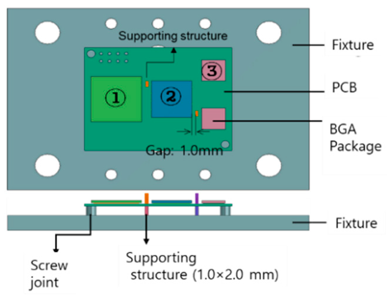
Figure 2 shows the test vehicle and the supporting fixture used in this study. As a typical option for modern portable electronics, we use a 6-layers PCB with 44.0 mm length, 34.0 mm width, and 0.6 mm thickness supported with two screws. Normally, four screws are used to avoid PCB deformation. However, recently the number of screws in mobile products decreases for the reasons of slim cost-effective design, and the PCB deformation is more pronounced when a small number of screws are used. Also, as shown in Figure 3 (left), the PCB is prepared using SR (solder resist), NSMD (non-solder mask defined), and OSP (organic solderability preservative) for surface finishing of Cu pads. After SAC305 solder reflow process, four BGA packages are surface mounted onto the PCB as shown in Figure 3 (right). The package size and the ball diameter/pitch are described in Table 1.
In order to apply different boundary conditions of solder joints in the BGA packages, three different aluminum fixtures are prepared as shown in Figure 4. In case of fixture I, the load imposed on BGA packages is only the PCB deformation from the shock impact. Fixture II is designed to reduce the PCB deformation without additional screws by locating the upper and lower supporting structures near to diagonal corners of the package ② as shown in Figure 2. fixture III is designed to consider the contact behavior between the package and the wall structure as a representative of rigid bracket or shield cans.
A board-level drop test setup is shown in Figure 5a. Each fixture with PBA is mounted to the drop table of the Lansmont® M23 drop tester (Lansmont, Shanghai, China). The drop table is raised to the specified height and dropped on the strike surface while measuring the g-level, pulse duration, and pulse shape. Multiple drops may be required while adjusting the drop height and the strike surface to achieve the specified g-levels and pulse duration. In this work, following the JEDEC standard JESD22-B111a, the pulse with 1500 g peak acceleration and 0.5 millisecond pulse duration (Figure 5b) were obtained and used as the input pulse [19]. In order to assess the effect of the fixture design on the reliability of the BGA packages, the event detector was used to constantly monitor the resistance of the daisy chained circuits throughout the test and record the number of drops to failure. 12 samples for fixture I, and 10 samples for fixtures II and III were used in the drop test with all BGA packages daisy chain connections to statistically determine drop reliability.
To measure PCB deformation, DIC (digital image correlation) and synchronized high-speed camera are used as shown in Figure 5a. High-speed digital cameras are set up to capture pictures of the board surface during the impact frame by frame, with a frequency of up to 10,000 frames per second. These images were then exported to the commercial software package ARAMIS® (v6.3.0, OMA Co., Daejeon, Korea, 2014) for solving full-field deformations, 3D shape, and the PCB strain. Previously, Park et al. demonstrated the utilization of DIC technique for measuring displacement of PBA and verified measurement accuracy [20].

2.2. Test Results

The out-of-plane deformation of the PCB in case of drop is always of most interest to the manufacturers as it relates to the stress causing the failure of the solder joints. It is commonly assumed, the thinner the PCB with higher PCB deflection, the shorter is the impact life of the package, meaning the higher stress in the solder joints. In this regard, a PBA with same BGA packages and 6 layers of 0.8 mm thickness was prepared as a reference. Then, both 0.6 mm thick and 0.8 mm thick PCB with fixture I were translated into the drop test until the solder joint failure. At the same time, DIC measurement took place and provided contour plot of the out-of-plane displacement and time history data during shock impact as the load is applied. Figure 6 shows the out-of-plane displacement contours for each PCB thickness with fixture I when both PBAs are experiencing the maximum deflection right after the shock table hits the strike surface. These data were taken at the intervals of 1.0 millisecond for 0.8 mm thick PCB and 1.2 millisecond for 0.6 mm thick PCB, respectively. From Figure 6, the screw fastened locations can be recognized whereas the unfastened PCB corners deflect the most. In addition, the center of the PBA is expected to be subject to severe bending deformation after the shock impact load where BGA package ② is attached and the outer solder joints of the package ② are noticed as the area where the failure occurs. Therefore, Figure 7 shows the time history of the out-of-plane displacement at the center point of BGA package ② for 0.6 mm and 0.8 mm thick PCBs. As the PCB gets thinner, the maximum displacement after the impact increases, and the frequency decreases due to lower rigidity of the PCB. The BGA package ② on 0.6 mm thick PCB is deflected downward 1.2 mm at the impact and upward 1.0 mm at the bouncing back whereas 0.8 mm PCB is deflected downward 0.75 mm and upward 0.65 mm. These results naturally indicate that the drop impact life for the BGA package ② with 0.6 mm PCB is shorter.
In order to investigate the effect of the fixture type on the reliability of the BGA package ②, an event detector was applied to constantly monitor the resistance of the daisy chained circuits throughout the test and record the number of drops to failure. The drop test was conducted for 12 samples of fixture I, and 10 samples of fixtures II and III. The reliability analysis of the drops to failure from the drop tests was carried out using a two parameter Weibull distribution plot as shown in Equation (1).
F ( t ) = 1 e ( t η ) β
where F(t) is the cumulative failure distribution function, η is referred to as the characteristic life and is the number of failure cycles at which 63.2% of the BGA package failed, and β is the shape parameter.
The drop reliability of the BGA package ② for each fixture I, II, III is shown as a Weibull distribution in Figure 8. According to the result, the BGA package ② with fixture III exhibits higher reliability than the other two, and fixture I shows the lowest one. This is because fixtures III and II have more structures than fixture I that minimize the PBA deflection. Figure 8 can be interpreted statistically as shown in Table 2. From the Equation (1), scale parameters (η) for each fixture I, II, III are found 22.8, 34.2, 159 drops, respectively, as a characteristic life under the drop event. Also, the shape parameters (β) for all fixtures is between 1 to 1.3 which means BGA failures are attributed to wear damages by accumulated plastic energy from repeated drop impact. Anderson-Darling values show the goodness of data fit with Weibull plots using the Minitab program.
After sequential drop tests, some PBAs are inspected for BGA failure. The cross-section of the solder ball array is analyzed; the representative image for BGA package ② is shown in Figure 9. All failures are found to be IMC cracks developed in the outer solder joints of the package. In fact, all packages show mostly the interfacial failure either between the package and the solder joints (Figure 9a,c) or between the solder joints and the PCB pad (Figure 9b). Since the IMC layer is so brittle, the failure caused by the shock impact is initiated around the IMC layer.
Table 3 outlines the characteristic life for all BGA packages, including BGA package ①, and all fixtures. Particularly, 0.8 mm and 0.6 mm thick PCB with fixture I are compared. As discussed earlier, 0.8 mm thick PCB with fixture I exhibits longer characteristic life which means higher drop reliability. This is obviously because of the smaller deflection as compared to 0.6 mm thick PCB with fixture I. It should be noticed that the BGA package ③ is not included since it rarely fails within 1000 times of drop life due to smaller package size effect. Between BGA package ① and ②, package ② has a lower drop reliability for all cases except for fixture III. This is because fixture III has a wall structure that allows PBA contact when it bounces back which results in eventually less magnitude of the PBA deformation. Also, when PBA bounces back, the contact area between the wall structure and the BGA package ① protects the contact of the BGA package ② because the height and ball diameter of the package ① are larger than those of the package ②. Since IC packages take more strain energy on largely deformed PCB, suppression of the PCB deformation results in higher drop impact reliability of the solder joints.

3. FEA Method

Stress analysis of the solder joints is needed to investigate how failure mechanism is related to PCB deflections. A 3D FEA model was built using PAM-CRASH commercial software package as shown in Figure 10. PCB and BGA packages including solder joints are represented with a solid model. Solder joints at the corner referred to as A in Figure 10 were modelled in detail, and the other solder joints referred to as B and C were modelled as octagonal columns. PCB, Cu pad, and package (epoxy mold compound) are assumed to have isotropic and elastic material properties as shown in Table 4. As many researches, the material property behavior of the solder joints are generally assumed visco-plastic such as in Anand’s model, which is more relevant to simulate thermal cyclic loading [21,22,23,24,25]. However, the solder joints were to be considered as elasto-plastic at high strain rates [26]. Therefore, Ramberg-Osgood model for SAC305 was used to implement more accurate simulation of the solder joint during the drop test as shown in Figure 11. Also, the loading condition, 1500 g peak acceleration and 0.5 ms pulse duration (Figure 5b), is imposed at the fixture shown in Figure 2.

3.1. Validation of the Drop FEA Model

To validate 3D FEA model for drop simulation, the drop test was carried out for both the bare PCB (0.8 mm thickness) and the PBA (0.6 mm thickness) with fixture I, and dynamic responses were acquired using the DIC technique.
First, the bare PCB (0.8 mm thickness) response to the drop test is examined for fixture I. Figure 12 compares dynamic responses of the bare PCB from the drop test and the corresponding FEA simulation result. According to Figure 12a, first few displacement peaks are well matched while there is some discrepancy after about 4.0 ms due to PCB manufacturing defects. However, the first two peaks of the PCB deflection under the drop event are the most critical because the solder joints undergo the maximum stresses during this stage. In addition, Figure 12b provides both quantitative and qualitative validation results by showing similar out-of-plane contour plots between the FEA and the DIC result.
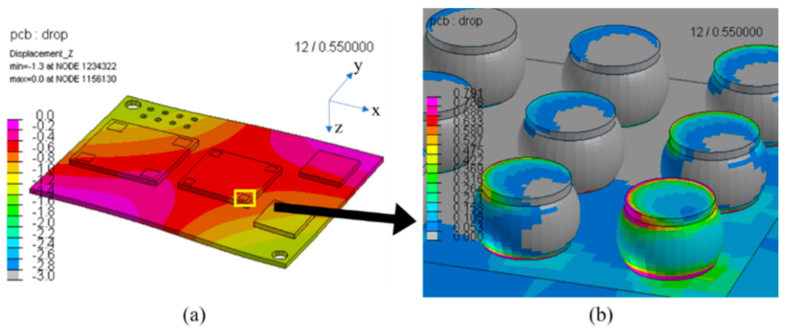
Second, from FEA simulation of the PBA (0.6 mm thick PCB) with fixture I, the maximum principal stress location is compared with the failure location. As a result, the PBA deflects the most at 0.55 ms after shock impact is applied, and the out-of-plane displacement contour and the principal stress distribution for the package ② are shown in Figure 13. The maximum stress occurs around Cu pad of the PCB at the corner of the package ② which means the failure mode is identical to that shown in Figure 9. Therefore, the 3D FEA model for the drop test is feasible for parametric studies providing reasonable guidelines to enhance drop reliability.

3.2. Beam Model vs. Solid Model

Initially, 3D FEA model was built to analyze the stresses of the BGA solder joints under the drop test. However, since we use solid model for all components, computation with the specified mesh sizes takes about 110 h. This is because the aspect ratio is too high between the components, for instance solder joint and PCB in our case. The mesh density was defined differently according to the dimension of components. Also, time-step should be very small for smaller meshes. Therefore, we tried to use spring-beam elements instead of solid element not only to achieve computational efficiency, but also to simplify mesh generation as shown in Figure 14. Basically, a spring-beam element connects two projection nodes at each surface (see Figure 14a), and multi-point kinematic constraints connect the beam to the meshes (see Figure 14b). Therefore, replacing the solder joint from a 3D element (solid model) to 1D element (beam model), can significantly reduce the aspect ratios of the elements for entire model. The spring beam element can calculate tension and moment to replace the solid element.
According to the solder joints geometry, solid model and beam model are considered for element type as shown in Figure 15. In addition, Table 5 describes the comparison between the two models in terms of computing efficiency. Larger mesh size shortens the number of the elements that results in dramatic reduction of the required computing time. To confirm the feasibility of the beam model, first, the dynamic responses at the BGA package ② with fixture I are compared for both the models. Figure 16 shows the comparison of the solid model and the beam model for the BGA solder joint at 0.55 ms after impact loading. The displacement contour is shown in Figure 16a. The displacement response of the beam model almost matches that of the solid model. The discrepancy of the maximum out-of-plane displacement was found only 0.06 mm between the two models.
Next, the resulting force and the stress of solder joint is studied between the beam and the solid models. Since the beam model produces the moment followed by the force at the spring-beam element, the magnitude of the force is compared with the principal stress of the solid model as shown in Figure 16b. The maximum value occurs at the corner of the package, and the stress time response of the solid model coincides with the force time response of the beam model. Therefore, the beam element for the solder joint array can be used to assess the drop reliability of the BGA package.
Although the beam element cannot show the amount of the stress within each solder joint, it can provide the directional force and the moment of the beam. In fact, the solder joint undergoes repeated tensile and compressive force during the drop test, and the joint is usually weaker under tension rather than compression. Therefore, the maximum tensile strain of the beam element can be suggested as the solder joint failure criteria. Using the beam model, FEA simulations for the PBA with fixtures II and III were sequentially carried out as well. The tensile strain responses of the package ② among the three fixtures are compared as shown in Figure 17. The BGA package ② with fixture I experiences the biggest amount of the tensile strain (0.35). Fixture II experiences the average amount of the tensile strain (0.2). Fixture III experiences the smallest amount of the tensile strain (0.03) among the three fixtures. This also explains the characteristic life of the BGA solder joints with fixtures I, II, and III that are 22.9, 34.2, and 159 drops to failure, respectively.

4. Conclusions

In this paper, the drop reliability of the BGA packages on the PBA mounted with three difference fixtures is investigated and compared from the results of the drop tests. The results were analyzed with a Weibull plot using scale and shape factors as two parameters. In addition, dynamic responses of 0.6 mm and 0.8 mm thickness PBA with fixture I are compared using the DIC method. In this result, thinner PBA deflects more and has shorter characteristic life (drops to failure) under the drop impact event. Also, when comparing the three fixtures, the BGA package jointed in the middle of the PBA shows shorter impact life, and the failure mode mostly occurs at the most outer solder joints. This is because more stress concentration is imposed by the repeated out-of-plane deformation. Fixtures II and III have longer impact life compared to fixture I because of more constrains on the rigid body motion of the BGA package ②.
Also, FEA modeling was used to investigate the dynamic response of the PBA and experimentally verified using the DIC method to compare the failure modes. The 3D full-field FEA model was performed to analyze stress distributions of the solder joint where the failure occurs. Further, the simple beam model was used for failure modeling of the solder joint array, and compared with the detailed solid model regarding numerical accuracy and computational efficiency. The maximum tensile strain of the beam element was chosen as a failure criterion, and compared with the resulting drop life among three different loading conditions. It was confirmed from the dynamic response and its corresponding strain that the simple beam model can predict the drop reliability of the solder joint array induced by the drop impact. Also, the beam model dramatically shortens the required computational time which means that effective parametric study is possible to find the optimal layout of the BGA packages and assembly conditions.

Author Contributions

Conceptualization, J.B.K. and S.C.; Methodology, J.B.K.; Validation, S.C.; Formal Analysis, S.C.; Investigation, J.B.K. and S.C.; Data Curation, S.C.; Writing—Original Draft Preparation, S.C.; Writing—Review & Editing, J.B.K.; Funding Acquisition, J.B.K. All authors have read and agreed to the published version of the manuscript.

Funding

This study was supported by the National Research Foundation of Korea (NRF) grant funded by the Korea government (Ministry of Science and ICT) (No. NRF-2018R1C1B5045726) and Korea Institute for Advancement of Technology (KIAT) grant funded by the Korea Government (MOTIE) (P0002092, The Competency Development Program for Industry Specialist).

Acknowledgments

The authors would like to acknowledge the technical support of HANKOOK ESI Co., Ltd. for drop simulation.

Conflicts of Interest

The authors declare no conflict of interest.

References

  1. Zhou, C.Y.; Yu, T.X.; Lee, R.S. Drop/impact tests and analysis of typical portable electronic devices. Int. J. Mech. Sci. 2008, 50, 905–917. [Google Scholar] [CrossRef]
  2. Xu, Y.; Li, M.; Li, C. The Research of Test System of Notebook Use Reliability. Adv. Mater. Res. 2013, 684, 630–633. [Google Scholar] [CrossRef]
  3. Yau, Y.H.; Hua, S.N. A Comprehensive Review of Drop Impact Modeling on Portable Electronic Devices. Appl. Mech. Rev. 2011, 64, 020803. [Google Scholar] [CrossRef] [Green Version]
  4. Shnawah, D.A.; Sabri, M.F.M.; Badruddin, I.A. A review on thermal cycling and drop impact reliability of SAC solder joint in portable electronic products. Microelectron. Reliab. 2012, 52, 90–99. [Google Scholar] [CrossRef]
  5. Singh, B.; Menezes, G.; McCann, S.; Jayaram, V.; Ray, U.; Sundaram, V.; Pulugurtha, R.; Smet, V.; Tummala, R. Board-Level Thermal Cycling and Drop-Test Reliability of Large, Ultrathin Glass BGA Packages for Smart Mobile Applications, IEEE Transactions on Components. Packag. Manuf. Technol. 2017, 7, 726–733. [Google Scholar] [CrossRef]
  6. Gu, J.; Lei, Y.; Lin, J.; Fu, H.; Wu, Z. The Failure Models of Lead Free Sn-3.0Ag-0.5Cu Solder Joint Reliability Under Low-G and High-G Drop Impact. J. Electron. Mater. 2017, 46, 1396–1404. [Google Scholar] [CrossRef]
  7. Yu, D.; Kwak, J.; Park, S.; Chung, S.; Yoon, J. Effect of Shield-Can on Dynamic Response of Board-Level Assembly. J. Electron. Packag. 2012, 134, 031010. [Google Scholar] [CrossRef] [Green Version]
  8. Mishiro, K.; Ishikawa, S.; Abe, M.; Kumai, T.; Higashiguchi, Y.; Tsubone, K.I. Effect of the Drop Impact on BGA/CSP Package Reliability. Microelectron. Reliab. 2002, 42, 77–82. [Google Scholar] [CrossRef]
  9. Farris, A.; Pan, J.; Liddicoat, A.; Toleno, B.J.; Maslyk, D.; Shangguan, D.; Bath, J.; Willie, D.; Geiger, D.A. Drop Test Reliability of Lead-free Chip Scale Packages. In Proceedings of the 58th Electronic Components and Technology Conference, Lake Buena Vista, FL, USA, 27–30 May 2008; pp. 1173–1180. [Google Scholar]
  10. An, T.; Qin, F. Effects of the intermetallic compound microstructure on the tensile behavior of Sn3.0Ag0.5Cu/Cu solder joint under various strain rates. Microelectron. Reliab. 2014, 54, 932–938. [Google Scholar] [CrossRef]
  11. Jiang, N.; Zhang, L.; Liu, Z.; Sun, L.; Long, W.; He, P.; Xiong, M.; Zhao, M. Reliability issues of lead-free solder joints in electronic devices. Sci. Technol. Adv. Mater. 2019, 20, 876–901. [Google Scholar] [CrossRef] [Green Version]
  12. Shao, J.; Zhang, H.; Chen, B. Experimental Study on the Reliability of PBGA Electronic Packaging under Shock Loading. Electronics 2019, 8, 279. [Google Scholar] [CrossRef] [Green Version]
  13. Wu, M.L.; Lan, J.S. Reliability and failure analysis of SAC 105 and SAC 1205N lead-free solder alloys during drop test events. Microelectron. Reliab. 2018, 80, 213–222. [Google Scholar] [CrossRef]
  14. Xu, Z.J.; Jiang, T.; Song, F.B.; Lo, J.C.C.; Lee, S.W.R. Modeling of Board Level Solder Joint Reliability under Mechanical Drop Test with the Consideration of Plastic Strain Hardening of Lead-free Solder. In Components, Packaging, and Manufacturing Technology Symposium, Japan; IEEE: Piscataway, NJ, USA, 2010; pp. 1–4. [Google Scholar]
  15. Zhu, L.; Marcinkiewicz, W. Drop Impact Reliability Analysis of CSP Packages at Board and Product Levels through Modeling Approaches. IEEE Trans. Compon. Packag. Technol. 2005, 28, 449–456. [Google Scholar]
  16. Tee, T.Y.; Ng, H.S.; Lim, C.T.; Pek, E.; Zhong, Z. Drop test and Impact life prediction model for QFN packages. J. SMT 2003, 16, 31–39. [Google Scholar]
  17. Tee, T.Y.; Ng, H.S.; Lim, C.T.; Pek, E.; Zhong, Z. Impact Life prediction modeling of TFBGA packages under board level drop test. Microelectron. Reliab. 2004, 44, 1131–1142. [Google Scholar] [CrossRef]
  18. Nguyen, T.T.; Park, S. Elasto-plastic behavior of actual SAC solder joints for drop test modeling. Microelectron. Reliab. 2011, 51, 2126–2129. [Google Scholar] [CrossRef]
  19. JEDEC. Board Level Drop Test Methods of Components for Handheld Electronic Products, JESD22-B111a; JEDEC: Arlington, VA, USA, 2016. [Google Scholar]
  20. Park, S.; Shah, C.; Kwak, J.B.; Jang, C.S.; Chung, S.W.; Pitarresi, J.M. Measurement of Transient Dynamic Response of Circuit Boards of a Handheld Device During Drop Using 3D Digital Image Correlation. J. Electron. Packag. 2008, 130, 044502. [Google Scholar] [CrossRef]
  21. Wang, G.Z.; Cheng, Z.N.; Becker, K.; Wilde, J. Applying Anand Model to Represent the Viscoplastic Deformation Behavior of Solder Alloys. J. Electron. Packag. 2001, 123, 247–253. [Google Scholar] [CrossRef]
  22. Li, X.; Wang, Z. Thermo-fatigue life evaluation of SnAgCu solder joints in flip chip assemblies. J. Mater. Process. Technol. 2007, 183, 6–12. [Google Scholar] [CrossRef]
  23. Amalu, E.H.; Ekere, N.N. High temperature reliability of lead-free solder joints in a flip chip assembly. J. Mater. Process. Technol. 2012, 212, 471–483. [Google Scholar] [CrossRef]
  24. Amalu, E.H.; Ekere, N.N. Modelling evaluation of Garofalo-Arrhenius creep relation for lead-free solder joints in surface mount electronic component assemblies. J. Manuf. Syst. 2016, 39, 9–23. [Google Scholar] [CrossRef]
  25. Kang, J.S. Parametric study of warpage in PBGA packages. Int. J. Adv. Manuf. Technol. 2020, 107, 4213–4219. [Google Scholar] [CrossRef]
  26. Iqbal, N.; Xue, P.; Wang, B.; Li, Y. On the high strain rate behavior of 63-37 Sn-Pb eutectic solders with temperature effects. Int. J. Impact Eng. 2014, 74, 126–131. [Google Scholar] [CrossRef] [Green Version]
Figure 1. Various printed board assembly (PBA) mounting structures for portable electronics.
Electronics 09 01515 g001
Figure 2. Test vehicle and supporting fixture.
Electronics 09 01515 g002
Figure 3. Test vehicle with various ball grid array (BGA) packages before and after reflow process.
Electronics 09 01515 g003
Figure 4. Schematic of three fixtures for various BGA boundary conditions.
Electronics 09 01515 g004
Figure 5. Experimental setup: (a) drop test system and digital image correlation (DIC) measurement equipment, (b) half-sine input pulse.
Electronics 09 01515 g005
Figure 6. Out-of-plane displacement contour plots for PBA with fixture I.
Electronics 09 01515 g006
Figure 7. Time series of the out-of-plane displacement of the BGA package ② with fixture I.
Electronics 09 01515 g007
Figure 8. Weibull distribution of the drops to failure for BGA packages ② with various fixtures.
Electronics 09 01515 g008
Figure 9. Failure analysis of the BGA package ②. (a) crack failure between Package and BGA, (b) crack failure between BGA and PCB, (c) crack propagating between Package and BGA.
Electronics 09 01515 g009
Figure 10. 3D finite element analysis (FEA) model.
Electronics 09 01515 g010
Figure 11. Stress-strain curve for SAC305 at high strain rate (drop shock).
Electronics 09 01515 g011
Figure 12. Drop response of the bare PCB (0.8 mm thickness) with fixture I: (a) Displacement with respect to time, (b) out-of-plane deformation contour plot for FEA and DIC test results.
Electronics 09 01515 g012
Figure 13. FEA result of the PBA (0.6 mm thick PCB) with fixture I: (a) out-of-plane deformation contour, (b) principal stress (GPa) distribution under BGA package ②.
Electronics 09 01515 g013
Figure 14. Beam model: (a) spring-beam element connection between the two surfaces, (b) multi-point kinematic constraint.
Electronics 09 01515 g014
Figure 15. Solder joints modeling. (a) Solid model (3D element); (b) beam model (1D element).
Electronics 09 01515 g015
Figure 16. Solid model and beam model for the solder joint. (a) Displacement contour plots at 0.55 ms; (b) Principal stress (solid model) and force (beam model).
Electronics 09 01515 g016
Figure 17. Time response of the tensile strain for all fixtures.
Electronics 09 01515 g017
Table 1. BGA package specification.
BGA PackageOuter Size (mm)Ball Diameter (mm)Ball Pitch (mm)Number of Balls (ea)Array Type
15.0 × 15.0 × 1.210.40.8170Peripheral
12.0 × 12.0 × 1.150.30.5222Peripheral
7.0 × 7.0 × 1.10.30.5123Full
Table 2. Analysis of the Weibull distribution plot for BGA package ②.
FixturesN (Number of Samples)Scale Parameter (η) Characteristic LifeShape Parameter (β)AD (Anderson-Darling)
fixture I1222.80.980.486
fixture II1034.21.280.339
fixture III101591.290.509
Table 3. Characteristic life (number of drops to failure) of the BGA solder joints with various fixtures.
BGA PackageFixture I
(0.8 mm Thick PCB)
Fixture I
(0.6 mm Thick PCB)
Fixture II
(0.6 mm Thick PCB)
Fixture III
(0.6 mm Thick PCB)
63.925.2123.791.5
32.722.934.2159
Table 4. Mechanical properties of the components.
ComponentsDensity (Kg/mm3)Elastic Modulus (GPa)Poisson’s Ratio
BGA Package (EMC)1.89 × 10−6280.35
Cu pad8.94 × 10−61170.34
Solder joints7.44 × 10−6900.42
PCB1.91 × 10−616.80.36
Table 5. Comparison of the solid element and the beam element in FEA model.
FEA ModelSolid ElementBeam Element
Minimum Mesh Size (mm)0.0038160.16
Number of Element (ea)755,28890,507
Time Step (ms)3.14 × 10−71.86 × 10−5
Elapsed time (s) (12 core CPU)403,600 (113 h)2415 (40 min)