Article

Multibit-Generating Pulsewidth-Based Memristive-PUF Structure and Circuit Implementation

1
Department of Electronic and Electrical Engineering, Ewha Womans University, Seoul 03760, Korea
2
Department of Electrical and Computer Engineering, Seoul National University, Seoul 08826, Korea
*
Authors to whom correspondence should be addressed.
Electronics 2020, 9(9), 1446; https://doi.org/10.3390/electronics9091446
Submission received: 7 August 2020 / Revised: 29 August 2020 / Accepted: 1 September 2020 / Published: 4 September 2020
(This article belongs to the Special Issue Cyber Security for Internet of Things)

Abstract

:
As Internet of Things (IoT) devices have evolved, physical unclonable functions (PUFs) have become a popular solution for hardware security. In particular, memristor devices are receiving attention as suitable candidates for reliable PUFs because they can be integrated into nano-cross point array circuits with ultra-high efficiency. However, it has been found that typical 1-bit generating PUFs consume too many challenge–response pairs (CRPs) to generate a single response. This issue has to be overcome to construct a strong and reliable PUF with a large number of valid CRPs. We suggest a bank design and quantizing entropy source method for constructing a multibit-generating PUF. In this paper, we propose a new pulsewidth-based memristive PUF (pm-PUF) architecture that incorporates analog memristor devices and a nano-cross point array. We describe the architecture’s circuit implementation and its operating process in detail. We also evaluate the inter and intra performances of the pm-PUF in terms of randomness, diffuseness, uniqueness, and steadiness to show that the proposed pm-PUF will be a promising solution for a high-density hardware security system.

1. Introduction

As Internet of Things (IoT) applications have rapidly proliferated, connected IoT device designs have trended toward sharing private data during communication; the shared data are not always secure from advanced hacking technology. Hardware security systems have been suggested; one of the solutions is using non-volatile memory (NVM) with its high density, reduced power consumption, and non-volatility. However, this scheme proves to be vulnerable to invasive physical attacks on systems to reveal their secret information [1].
To defeat such security threats, physical unclonable functions (PUFs) have been gaining attention as a promising component for trustworthy communication. PUFs utilize inherent physical variations that occur naturally during hardware device manufacturing and that are theoretically impossible to duplicate because some of them are unpredictable and uncontrollable [2]. These variations are the source of entropy that makes the responses unique.
In general, PUFs implement a challenge–response protocol wherein a challenge is applied to a PUF and a corresponding response is generated. The specific challenge and its corresponding response form a single challenge–response pair (CRP). The response is a very complex function of the given challenge and the unique physical features of the PUF [3]. For example, the responses to different challenges have to be different for a given PUF. In addition, for a given challenge applied to different PUFs, different responses should be generated due to the distinguishing property of each PUF instance. These constraints allow a set of CRPs to be regarded as the fingerprint of a PUF device that can be used in applications such as authentication, identification, and key generation [4].
Various PUF structures have been proposed since the concept of a PUF was first introduced [5,6,7,8,9]. PUFs can be classified as conventional PUFs that use traditional Complementary Metal Oxide Semiconductor (CMOS) devices or nanoelectronic PUFs which use nano-scale devices [6]. Conventional PUFs such as ring oscillator PUFs [7], latch PUFs [8], and arbiter PUFs [9] seemed appealing because of their easy construction. However, with the technology trending toward smaller feature sizes, CMOS devices with their CMOS-based PUF structures are likely to face future physical limitations on scaling down [10].
Recently, new PUF structures that incorporate nanoelectronics such as magnetic random-access memory (MRAM) [11], phase-change memory (PCM) [12], and memristors [13] have emerged to overcome CMOS limitations. In particular, memristors are expected to be a winning candidate owing to their higher sensitivity to the fabrication process and wider device-to-device variations than conventional PUFs. Moreover, the memristor, as a two-terminal resistive memory device, has the advantage of ultra-high integration density and low cost when realized as a cross-point array architecture [14].
Memristor-based PUFs have a finite number of CRPs corresponding to the limited number of memristor cells. To build a strong PUF for trustworthy communication, it is necessary to have a large number of valid CRPs [15]. However, in most cases, PUF structures generate a single bit for a given challenge bits and multiple CRPs are consumed to generate a single multibit key [16,17]. The single-bit generating method not only wastes valid CRPs but also increases the required time for manufacturers to generate the CRP table. This means there is a need to develop a new structure to generate multibit responses. On the other hand, for a given array size, generating multiple bits per challenge is likely to have less dynamic CRPs since the combinations of memristor cells are limited. Hence, it is important to increase the inherent randomness of the individual cell.
To deal with these issues, we propose a novel multibit-generating pulsewidth-based memristive-PUF (pm-PUF) structure that combines nano-cross point arrays and multiple subarrays in a design that generates multibit responses. A summary of the main contributions of this study is as follows:
  • We present the electrical characteristics of an analog memristor model exposed to varied numbers of pulses with different pulsewidths and show that this memristor model is beneficial for wide variations.
  • We propose a new structure for a memristor-based PUF that utilizes fabrication variations that are physically inherent in nanoelectronic devices. A practical bank design is suggested for a multibit-generating pm-PUF.
  • The circuit implementation of the proposed pm-PUF architecture and its operation are described in detail.
  • The multiple bits stored in a single pm-PUF cell by quantization resolve the problem of wasted CRPs, dramatically reducing the pulse cycles required to generate them.
  • We report on a circuit simulation with HSPICE to demonstrate the unique performance of pm-PUFs in terms of randomness, diffuseness, uniqueness, and steadiness. The evaluation methods are also explained.
The rest of this study is organized as follows. Section 2 presents the memristor model and a practical bank design. We also present the proposed pm-PUF architecture and describe its operation in detail in this section. In Section 3, we analyze the performance of the pm-PUF. In Section 4, we compare the pm-PUF with other PUFs. We conclude in Section 5 with a discussion of the results and future work.

2. Materials and Methods

2.1. Cross-Point Array and Memristor Model

Cross-point array structures have attracted a lot of attention for their high device density, compatibility with existing CMOS technologies, and simple implementation of devices. Cross-point arrays typically consist of the horizontal rows and perpendicular columns. Each column is stacked on the rows and devices can be implemented at each junction. When a row and a column are selected, the device located at the junction is also selected to be read by applying a read voltage between the connected lines. In contrast, the unselected lines are floating and the unselected devices connected to them are not read. In this study, T a 2 O 5 memristors are implemented in a cross-point array, as shown in Figure 1. The figure shows that when a row and column are selected, read current (shown in red) flows through the selected device (also in red) at a level that depends on the cell’s resistance [18,19].
Several two-terminal nanoelectronic devices including memristors have recently emerged for use in cross-point arrays. For memristors whose behavior is based on filamentary switching, random manufacturing variations in thickness, doping concentrations, and forming directly affect the conductance of each unit produced [20].
In Figure 1b, the black diamond-shaped values are experimental data from a T a 2 O 5 memristor [21]. The red line in the figure shows that the simulated results from our Verilog-A memristor model conform well to the experimental data. The memristor device model was also used for applications such as neuromorphic systems in our previous work [22,23,24,25]. To calibrate the memristor, we used the generalized memristive device spice model [26] where the memristor current is represented by the hyperbolic sine function, as shown in Equation (1). The amplitude parameters a 1 and a 2 cause different increases in the memristor current depending on the polarity of the input voltage V(t) and its effect as represented by the parameter b.
I ( t )   =   { a 1 x ( t ) sinh ( b V ( t ) ) ,         V ( t ) 0 a 2 x ( t ) sinh ( b V ( t ) ) ,         V ( t ) < 0
The memristor current also depends on the state variable x(t) which directly impacts the conductivity of the device. The state variable has a value between 0 and 1. Equation (2) shows that the change in the state variable is based on two functions: g(V(t)) and f(x(t)).
d x d t   =   g ( V ( t ) ) f ( x ( t ) )
Equation (3) shows that a change in resistance only occurs when either the positive threshold V p or the negative threshold V n is exceeded. A p and A n determine the impact of the function g(V(t)). Equations (4) and (5) show that the amount of conductance change is limited as the state variable gets closer to the boundaries x n and x p . The decaying rate can be adjusted with the parameters α n and α p .
g ( V ( t ) )   = { A p ( e V ( t ) e V p ) ,         V ( t ) > V p A n ( e V ( t ) e V n ) ,         V ( t ) < V n 0 ,     V n   V ( t )   V p  
f ( x ( t ) ) = { e α n ( x + x n 1 ) w n ( x , x n ) ,         x 1 x n 1 ,                       x > 1 x n  
f ( x ( t ) )   =   { e α p ( x x p ) w p ( x , x p ) ,         x x p 1 ,                       x < x p  
w n ( x , x n )   = x 1 x n
w p ( x , x p )   = x p x 1 x p   +   1
The functions w n and w p in Equations (6) and (7) keep the state variable value between 0 and 1. The model parameters used for calibration in this study are listed in Table 1.

2.2. Initial Distributions

Memristor electrical behavior can be regarded as digital or analog resistive switching. Digital switching devices show abrupt resistive transitions during SET and RESET operations. In contrast, analog switching devices such as the T a 2 O 5 memristor characterized in Figure 1b exhibit a gradual current change as consecutive electrical inputs are applied, a behavior that is substantially different than the abrupt current jump exhibited by digital switching devices [27]. Figure 2a illustrates the resistance change of the analog memristor model we used in this study for 20-, 50-, and 100-ns pulses. The figure shows that wider pulses cause larger resistance decreases and more sequential pulses of the same width also decrease resistance.
In Figure 2b, the resistance distributions in the high resistive state (HRS) and the low resistive state (LRS) are compared to those resulting from a gradual SET and RESET transition induced by various pulses by using the characteristics of analog memristors described above.
The black bars show the initial resistance variation extracted from 4096 memristors in a 64 × 64 cross-point array. Half of the devices are SET and the other half are RESET; the blue bars show this resistance distribution. In contrast, the red bars exhibit the resistance variation when 64 different pulses are randomly applied to each memristor device. The influence of the pulses is added to the initial conductance of each device, resulting in random resistance variations which can be an entropy source for PUFs. It can be seen that the analog memristor model in gradual transition shows wider resistance distribution than it shows in two discrete states. In this study, wide entropy source variation is needed because it has to be quantized into several levels later to obtain multiple bits from a single cell value. However, since a transition to nano-size devices for the next generation is underway, wide die-to-die variation for a memory is a challenge that manufacturers want to resolve [28]. Hence, expanding the initial variations, minimum initial variations is considered in this study to maximize the effect of applied pulses.

2.3. Concept of Bank Design

The concept of combining multiple unit blocks to construct a large structure has been widely studied and applied. For example, a typical dynamic random-access memory (DRAM) system is divided into multiple blocks called banks that act as independent entities [29]. This structure serves multiple memory operations in parallel, which significantly reduces the total amount of time to generate the required outputs [30]. The structure can also be used to build a multibit-generating PUF by using multiple smaller PUFs since the response-generating processes can run in parallel. Furthermore, it has already been proven that combining small PUFs to build a large PUF results in better performance [31].
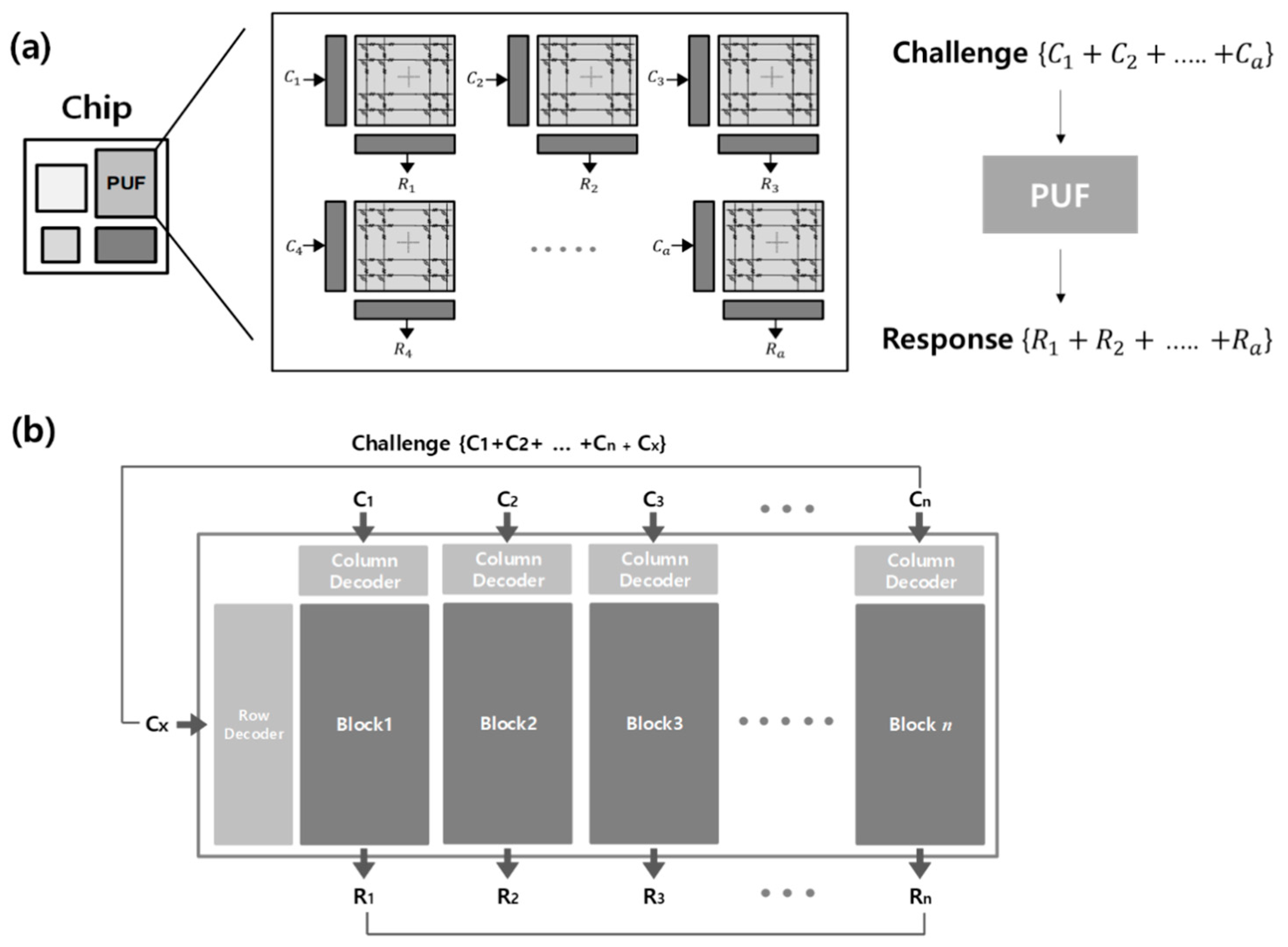
The proposed bank design is portrayed in Figure 3. The entire PUF consists of multiple small PUFs, each of which returns the bit strings ( R 1 , R 2 ,…,   R a ) in response to the corresponding challenge bit strings ( C 1 , C 2 ,…, C a ). The group of bit strings forms a single multibit response and challenge that is an overall input and output of the whole PUF as depicted in Figure 3a. Combining multiple PUFs in this way allows the production of multiple response bit strings in parallel which can significantly reduce the number of operating cycles needed to generate a multibit response. However, building a PUF from simply a combination of multiple PUFs increases area and total power consumption, thus a practical circuit implementation of bank design is suggested in Figure 3b. The entire array is divided into n subarrays and challenge bit strings are applied to each subarray through row and column decoders that select a particular cell out of the block. Since this practical structure is derived from a single cross-point array, each block operates from the same conditions, and a single row decoder is shared to select a row through n blocks. Therefore, fewer decoders are needed, saving area and power. Consequently, the corresponding response bit strings are generated from each block, and together they form a multibit response.

2.4. Pm-PUF Architecture

The circuit shown in Figure 4a is an implementation of the proposed pm-PUF architecture. The pm-PUF can be divided into four key parts: an MxN cross-point array, the control blocks, the decoder blocks, and the sense amplifier block. In the cross-point array of n subarrays, memristors are implemented at each junction and have the initial distribution of entropy resulting from the widely varied resistances of the gradual state transitions during the writing phase. The operation of the pm-PUF comprises a writing phase and a reading phase as determined by the read or write (R/W) signal. During the writing phase, the R/W signal is set to “0”, and, during the reading phase, the R/W signal is set to “1”.
The circuit operates initially with the control blocks which connect each row and column to the random pulse generator or the decoder block depending on the R/W signal. The control blocks comprise the row control circuitry in Figure 4b and the column control circuitry in Figure 4c. The control circuitry is connected to each of the rows and columns. It also controls the voltages applied to each of the memristors by applying the required voltages to the rows and columns. The decoder blocks determine whether a cell is read or not while the circuit is in its reading phase. The circuit implementation of decoder blocks is shown in Figure 4d,e. The row decoder circuitry is connected to one of the inputs of the control circuitry, but the column decoder circuitry, which is allocated per subarray, is connected to the gate of a switch that connects each column to the sense amplifier block. The inputs of the decoder blocks ( i n 1 , i n 2 ,…, i n x and I N 1 , I N 2 ,…, I N y ) are the challenge bits which contain the information about the addresses of the selected cells. The decoder for each subarray extracts the addresses and selects the cells to be read.
Here is how the pm-PUF operates in its two phases:
Writing phase. During the writing phase when the R/W and ON signals are set to “0”, the rows and columns are disconnected from the decoder blocks but connected to the random pulse generator. Pulses with different pulsewidths generated from the random pulse generator are applied to each row. The memristors are incrementally SET, and their conductance change is induced based on the applied pulsewidth. We also set the pulse amplitude higher than a threshold voltage by applying W N = 0, which ensures that the SET voltage is applied between the top and bottom electrodes. Next, W N = 0 is applied to each row and pulses are applied to each column resulting in a gradual RESET to the memristor devices. The result of these SET and RESET operations is that the array’s resistance variations, the entropy source of the pm-PUF, become widely distributed, as shown in Figure 2b.
Reading phase. During the reading phase, the R/W signal is set to “1”, connecting each row to the row decoder circuitry and column to the sense amplifier block with a switch that the column decoder circuitry controls. When a challenge for pm-PUF is applied, it is split into small challenge bit strings that are applied to the decoder of each subarray, providing the addresses of the selected cells. Then, the row and column decoders release output bits where one of the bits that corresponds to the selected row and column is “1” and the others are “0”. In the row decoder circuitry, the output of its AND gate connects a read voltage to each row when both of the inputs for AND gate (ON signal and the output of the decoder) are “1”. The ON signal is added to the decoder circuitry to block the AND gates before the address information is determined. When the decoder outputs are all delivered to the AND gates, the ON signal is set to “1” and the read voltage V r e a d is applied to the selected row, allowing read current to flow through the connected memristors. The read current of each memristor is likely to differ because it directly depends on the conductance determined during the writing phase. Likewise, in the column decoder circuitry, one of the switches connected to the selected column in each subarray is on and the other switches are off. Although current flows through the rest of the memristors connected to the selected row, a single column in each subarray is open for the current to flow to the sense amplifier block.
The sense amplifier block generates multibit responses by quantizing block output voltage. The sense amplifier block consists of multiple voltage sense amplifiers, as shown in Figure 5a. Sense amplifiers are one of the major components in a dense memory because they detect small voltage differences between two inputs and easily produce a binary output without additional circuits and processing. The current that flows from each block, which is related to the selected memristor’s resistance, is converted to a corresponding voltage by the load resistor R l o a d . The sense amplifiers compare the voltage with reference voltages to determine which sections the voltage value includes; each section is assigned to certain bits. The number of sense amplifiers required depends on the number of sections and response bits generated per block. The total CRPs are estimated as
C R P t o t a l   =   M   ×   ( N n ) n
where M is the number of rows and N is the number of columns. The parameter n is the number of blocks. The parameters can be altered for the required number of CRPs.
In our pm-PUF structure, the range of voltage values that the node V m can have is quantized into four sections, as shown in Figure 5b, to generate a 2-bit response for each subarray, thus three sense amplifiers are used. One of the quantized sections is allocated to each of the two-bit responses (00, 01, 10, and 11) and each section’s voltage boundaries are determined by three reference voltages of 227V, 234, and 241 mV. We investigated the voltage distribution of the possible combinations of selected cells and determined the reference voltages that divides the distribution equally into four sections. For example, the voltage value between 227 and 234 mV is assigned to the two-bit response “01”; any value over 241 mV is assigned to the two-bit response “11”.
By using the quantization blocks, more than one bit can be stored in a single cell, increasing the storage efficiency of a given array size [32]. As a result, the assigned response bits are gathered block by block to form a single multibit response. For example, if the voltage values from each of two blocks resulted in responses of “00” and “10”, the overall response would be “0010” obtained by concatenating the two-bit responses. Challenge–response behavior can be made more unpredictable with a more complex assignment method, but, in this paper, the simplest method of sequential assignment is used.

3. Results

3.1. Simulation Environment

We conducted a circuit simulation to build and evaluate the proposed pm-PUF. In this simulation, the pm-PUF was built using a 64 × 64 cross-point array with 1.2 Ω for line resistance and voltage sense amplifiers, as shown in Figure 5a. For the implementation of the bank design, the entire array was divided into eight subarrays of 64 × 8. Each memristor in the array followed the electrical characteristics of an experimentally measured T a 2 O 5 memristor device and was coded in Verilog-A for HSPICE circuit simulation using its generalized memristor model. Figure 1b shows that the simulation results of the Verilog model fit well with experimental results. It should be noted that minimum initial variations were used in these simulations to maximize the effect of pulses on variations. Pulse amplitude was set to 1.5 V, which is higher than the positive threshold voltage (=1 V), and the read voltage was set to 0.75 V, which is under the threshold voltage. The read voltage should not alter the resistance of the memristors. As a result of the circuit simulations with a 64 × 64 PM-PUF architecture, we obtained 2 30 possible CRPs using 30-bit challenges and two-bit responses combined from each subarray to form 16-bit responses.

3.2. Performance Evaluation

Performance evaluation is an essential process in the verification of practical and secure PUFs. There have been several methods proposed to measure PUF performance [33,34]. We selected the quantitative and statistical evaluation method proposed in [33] to analyze and quantitatively evaluate the performance of pm-PUF in terms of randomness, diffuseness, uniqueness, and steadiness. To evaluate intra-device performance, we applied 5500 different random challenges to a pm-PUF and measured randomness and diffuseness with the 5500 obtained CRPs. Uniqueness was evaluated for 100 different PUF instances. For steadiness, temperature and voltage deviations were tested with 256-bit responses. Temperature steadiness was measured at 0, 25, 50, and 85 °C with a constant supply voltage of 1.5 V. Voltage steadiness was measured at supply voltages of 1.4, 1.5, and 1.6 V at a constant room temperature of 25 °C
(1)
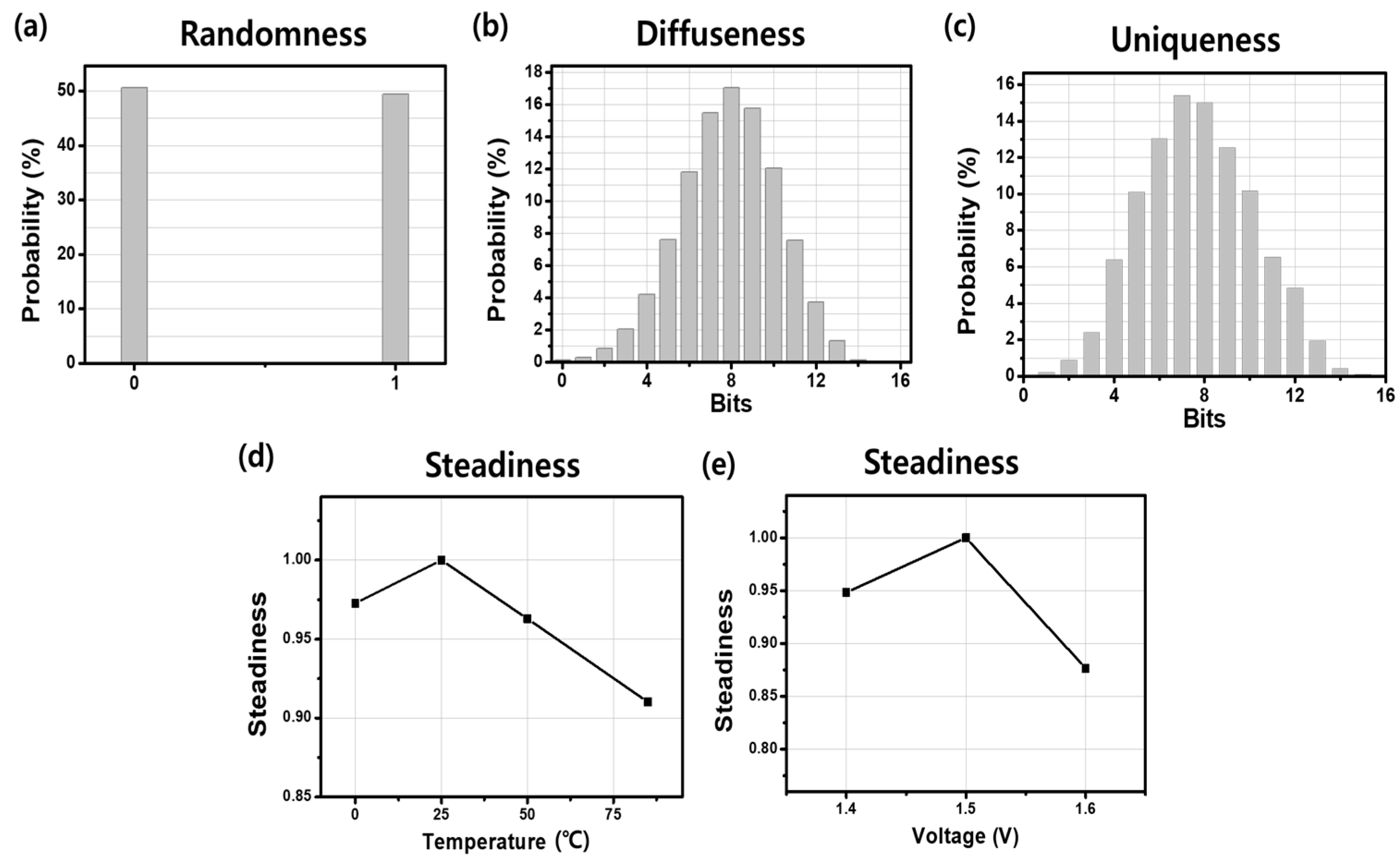
Randomness. Ideal “0” and “1” response bits generated from a PUF are expected to be equiprobable. Randomness is a measure of the balance of “0” and “1” values in the responses; Equations (9) and (10) define the randomness H n . Randomness is not related to the response generating mechanism because only the frequency of the two values is considered. To measure the frequency, we investigated 5500 responses obtained from the pm-PUF. The randomness of the pm-PUF is 0.9828 (98.28%), slightly lower than the ideal value of 1. This randomness corresponds to the probability of a “0” being 50.6% (49.4% for a “1”), as shown in Figure 6a. Therefore, almost 8 bits (8.096 bits) out of a 16-bit response are likely to be 1, which indicates that the pm-PUF shows a high degree of randomness.
H n   =   log 2 max ( p n ,   1 p n )
p n   =   1 K · T · L k = 1 K t = 1 T l = 1 L b n , k , t , l
where b n , k , t , l is the experimentally generated the lth bit of the kth response in device n in the tth test and p n is the relative frequency of 1 in all the response bits generated in device n.
(2)
Diffuseness. Diffuseness indicates the degree of difference among the responses obtained by applying different challenges to the same PUF. Diffuseness D n is determined by calculating the intra-hamming distance (intra-HD) of all possible responses from a PUF instance, as shown in Equations (11) and (12). To measure the diffuseness of the pm-PUF, we applied 5500 sets of random challenge bits to the PUF and obtained 5500 sets of 16-bit response bits. The distribution of intra-HDs among the obtained responses is shown in Figure 6b, and the mean of the HDs is 7.886 bits, which means 49.29%. The diffuseness of the pm-PUF as calculated with the equations below is 0.9871, which is close to the highest value of 1, thus the PM-PUF is expected to have high intra-device performance.
D n   =   1 L l = 1 L d n , l ( K / 2 ) 2
d n , l   =   i = 1 K 1 j = i + 1 K ( b n , i , l       b n , j , l )
where d n , l is the sum of HD of the possible bit combinations in b n , l .
(3)
Uniqueness. When the same challenges are applied to different PUF instances, the responses are expected to be different due to the variations of the PUFs. Uniqueness indicates the probability of difference between responses from the same challenge applied to different PUFs. Uniqueness U n can be calculated with the inter-HDs of responses from different PUFs and is defined below in Equation (13). To evaluate the uniqueness of the pm-PUF, we used 100 different PM-PUF instances, and the distribution of the number of different bits among the responses is shown in Figure 6c. The figure shows an inter-HD mean of 47.93%, which is 7.67 bits out of the 16-bit response. From Equation (13), the uniqueness of the pm-PUF is 0.9507, which is close to the ideal value of 1.
U n   =   4 K · L · N k = 1 K l = 1 L j = 1 , j n N ( b n , k , l       b j , k , l )
(4)
Steadiness. Steadiness (or reliability) indicates how stably a PUF operates. When the same challenge is applied to the same PUF several times, the responses are expected to be identical. However, due to environmental changes such as temperature and voltage shifts, steadiness can become a critical problem [35]. To evaluate the steadiness of the pm-PUF, we obtained a 256-bit response by repeatedly applying a set of random challenges at varied temperatures (0, 25, 50, and 85 °C) and voltages (1.4, 1.5, and 1.6 V) and by comparing the response bits. The reference response was obtained with 1.5 V at 25 °C. Steadiness can be measured based on the number of bit flips in the response bits during multiple tests. Device steadiness S n is defined as Equations (14) and (15). An ideal intra-HD between the responses under different operating conditions is 0 bits which corresponds to a steadiness of 1. The results are displayed in Figure 6d,e. Figure 6d shows that the worst steadiness of the pm-PUF is 0.9102 when the temperature is 85 °C. At the other temperatures, the pm-PUF also shows high steadiness (0.9726 at 0 °C and 0.9628 at 50 °C). In Figure 6e, the pm-PUF shows its worst voltage steadiness of 0.8765 for 1. 6V and 0.9484 for 1.4 V.
S n   =   1 K · L k = 1 K l = 1 L S n , k , l
S n , k , l   =   1 + log 2 max ( p n , k , l ,   1 p n , k , l )
where p n , k , l is the relative frequency of 1 in the lth bit of the kth response in device n and S n , k , l is the steadiness of the lth bit of the kth response expected to be generated in device n.

4. Discussion

We compared our pm-PUF with other memristor-based PUFs, as illustrated in Table 2. All PUFs are based on a new memristor that has wide variations. As mentioned in Section 2.2, the proposed pm-PUF utilizes the characteristics of analog memristors to make enhanced initial variations by using varied pulses, whereas the authors of [16] utilized a weak write mechanism to induce initial variations and the authors of [36] utilized the multilevel cell characteristics of RRAM. In Table 2, all PUFs have a randomness close to the ideal value of 50%. We compared the uniqueness of the method in [36] without bit shuffling because the pm-PUF incorporates a sequential assignment method. Uniqueness is not presented in [16].
In terms of total CRPs, the methods in [16,36] produce the same number of CRPs from their typical crossbar structures whereas the pm-PUF has significantly more CRPs. It is important to be able to improve the performance of a given PUF by increasing its number of CRPs.
The concept of reconfigurability has been suggested in [37] with the desire to generate different responses to the same challenge for the same PUF. In our pm-PUF design, responses are obtained from the voltage value at V m ; the value is a function of the output current, which is related to the resistance of selected memristors. Therefore, by altering the resistance distributions, a given PUF can be transformed into a new PUF with a new challenge–response behavior that makes it unique from others, yielding a new set of CRPs from the same PUF. Furthermore, additional reconfiguration circuits for the pm-PUF are not needed other than applying a RESET voltage to the memristors and rewriting them.
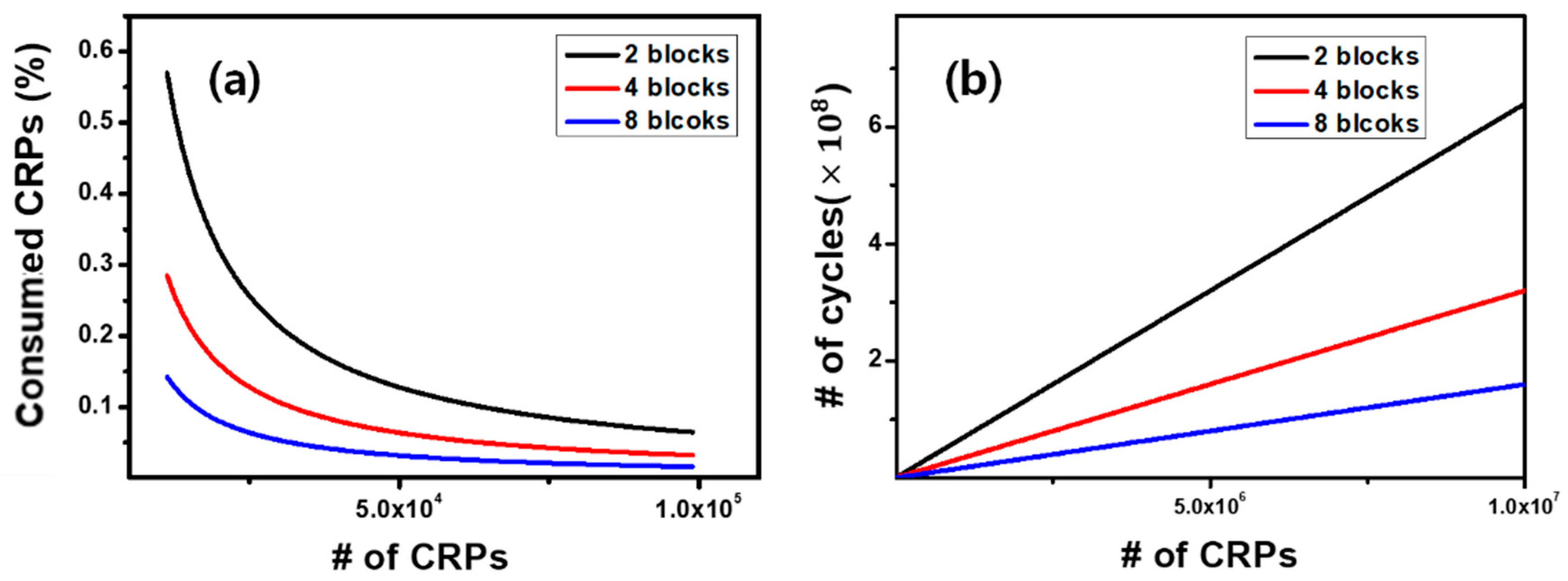
In contrast to other memristor-based PUF structures [16,17], the proposed pm-PUFs incorporate a bank design to create multibit responses in a single cycle. Figure 7 shows a promising property of the design that was investigated by employing circuit simulations. Three different pm-PUFs, where the total structure was comprised of two, four, or eight subarrays (blocks) each, were simulated, and responses from each PUF were combined to form a single 128-bit response. Figure 7a shows that the percentage of CRPs consumed to create a single response bit string is decreased overall as the total number of CRPs increases. It also can be seen that, the more the entire structure is divided, the fewer CRPs are wasted.
Challenges and responses from a PUF are saved in a CRP table and kept by manufacturers to be used in applications such as authentication. For manufacturers having the whole CRP table, less time to build CRP tables is beneficial. Figure 7b shows how many cycles are needed to build the complete CRP table; the PUFs with more subarrays require fewer cycles and take less time for a given CRP table.
In Figure 8, we compare a single bit-generating PUF [16,17] and the multibit pm-PUF responses. The cycle ratio (y-axis) represents the ratio of the total cycles needed to create a given number of response bits for a single bit-generating PUF compared with the pm-PUF. The highest cycle ratio value is 1 when both PUFs use the same number of cycles at one block with one quantized level. A PUF that has a lower cycle ratio shows optimized performance with more cycles saved. It can be seen that the cycle ratio is generally low and decreases significantly as the numbers of quantized levels and blocks increase.

5. Conclusions

In this paper, a pm-PUF architecture is newly proposed as a promising candidate for a PUF hardware security device. It showed that memristor-based PUFs have unique properties such as non-volatility, two modes of switching behavior, and ultra-high density in nano cross-point arrays. The study investigated the electrical characteristics of an analog memristor model subjected to different pulsewidths which resulted in wider device variations. The variations make it possible to store more than one bit in each memristor by quantizing output voltage levels arising from the variations. In our proposed pm-PUF, two-bit values are allocated to each of four quantized response voltage sections yielding two bits per subarray. More bits per section would reduce CRP consumption and production time, thus the development of a pm-PUF with more quantization levels would be a good subject for future work. We described a practical circuit implementation, simulated it with the HSPICE tool, and evaluated its performance. The simulation results show a 0.9828 randomness and a 0.9871 diffuseness, which are both near the ideal 1 value. Moreover, the results show a 0.9507 uniqueness result, 0.9102 temperature steadiness, and 0.8765 voltage steadiness for the worst case, indicating superior intra-device performance.

Author Contributions

Conceptualization, W.S.; software, S.C., D.K., and Y.C.; investigation, S.C., D.K., Y.C., W.S., and H.S.; writing—original draft preparation, S.C.; writing—review and editing, W.S. and H.S.; project administration, W.S.; and funding acquisition, H.S. All authors have read and agreed to the published version of the manuscript.

Funding

This research was supported by the Basic Science Research Program through the National Research Foundation of Korea (NRF) funded by the Ministry of Education, Science and Technology (Nos. NRF-2019R1A2C1084063 and NRF-2020R1I1A1A01065622).

Conflicts of Interest

The authors declare no conflict of interest.

References

  1. Shamsi, K.; Jin, Y. Security of emerging non-volatile memories: Attacks and defenses. In Proceedings of the 34th IEEE VLSI Test Symposium, Las Vegas, NV, USA, 25–27 April 2016; pp. 1–4. [Google Scholar]
  2. Herder, C.; Yu, M.; Koushanfar, F.; Devadas, S. Physical Unclonable Functions and Applications: A Tutorial. Proc. IEEE 2014, 102, 1126–1141. [Google Scholar] [CrossRef]
  3. Uddin, M.; Majumder, M.B.; Rose, G.S. Robustness Analysis of a Memristive Crossbar PUF against Modeling Attacks. IEEE Trans. Nanotechnol. 2017, 16, 396–405. [Google Scholar]
  4. Uddin, M.; Majumder, B.; Rose, G.S. Nanoelectronic Security Designs for Resource-Constrained Internet of Things Devices: Finding Security Solutions with Nanoelectronic Hardwares. IEEE Consum. Electron. Mag. 2018, 7, 15–22. [Google Scholar] [CrossRef]
  5. Pappu, R.; Recht, B.; Taylor, J.; Gershenfeld, N. Physical one-way functions. Science 2002, 297, 2026–2030. [Google Scholar] [CrossRef] [PubMed] [Green Version]
  6. Gao, Y.; Ranasinghe, D.C.; Al-Sarawi, S.F.; Kavehei, O.; Abbott, D. Emerging physical unclonable functions with nanotechnology. IEEE Access 2016, 4, 61–80. [Google Scholar] [CrossRef] [Green Version]
  7. Suh, G.E.; Devadas, S. Physical unclonable functions for device authentication and secret key generation. In Proceedings of the 44th ACM/IEEE Design Automation Conference 2017, San Diego, CA, USA, 4–8 June 2007; pp. 9–14. [Google Scholar]
  8. Ardakani, A.; Baradaran Shokouhi, S. A secure and area-efficient FPGA-based SR-Latch PUF. In Proceedings of the 8th International Symposium on Telecommunications (IST), Tehran, Iran, 27–28 September 2016; pp. 94–99. [Google Scholar]
  9. Gassend, B.; Clarke, D.; Van Dijk, M.; Devadas, D. Silicon physical random functions. In Proceedings of the 9th ACM Conference on Computer and Communications Security, Washington, DC, USA, 18–22 November 2002; pp. 148–160. [Google Scholar]
  10. Rostami, M.; Wendt, J.B.; Potkonjak, M.; Koushanfar, M. Quo vadis, PUF?: Trends and challenges of emerging physical-disorder based security. In Proceedings of the Design, Automation & Test in Europe Conference & Exhibition (DATE), Dresden, Germany, 21 April 2014; pp. 1–6. [Google Scholar]
  11. Huai, Y. Spin-transfer torque MRAM (STT-MRAM): Challenges and prospects. AAPPS Bull. 2008, 18, 33–40. [Google Scholar]
  12. Wong, H.-S.P.; Raoux, S.; Kim, S.; Liang, J.; Reifenberg, J.P.; Rajendran, B.; Asheghi, M.; Goodson, K.E. Phase Change Memory. Proc. IEEE 2010, 98, 2201–2227. [Google Scholar] [CrossRef]
  13. Strukov, D.; Snider, G.; Stewart, D. The missing memristor found. Nature 2008, 453, 80–83. [Google Scholar] [CrossRef] [PubMed]
  14. Kavehei, O.; Linn, E.; Nielen, L.; Tappertzhofen, S. An associative capacitive network based on nanoscale complementary resistive switches for memory-intensive computing. Nanoscale 2013, 5, 5119–5128. [Google Scholar] [CrossRef] [PubMed]
  15. Guajardo, J.; Kumar, S.S.; Schrijen, G.J.; Tuyls, P. FPGA Intrinsic PUFs and Their Use for IP Protection. In Cryptographic Hardware and Embedded Systems—CHES 2007; Paillier, P., Verbauwhede, I., Eds.; Springer: Berlin/Heidelberg, Germany, 2007; Volume 4727, pp. 43–80. [Google Scholar]
  16. Koeberl, P.; Kocabaş, Ü.; Sadeghi, A. Memristor PUFs: A new generation of memory-based Physically Unclonable Functions. In Proceedings of the 2013 Design, Automation & Test in Europe Conference & Exhibition (DATE), Grenoble, France, 18–22 March 2013; pp. 428–431. [Google Scholar]
  17. Rose, G.S.; McDonald, N.; Yan, L.; Wysocki, B. A write-time based memristive PUF for hardware security applications. In Proceedings of the IEEE/ACM International Conference on Computer-Aided Design (ICCAD), San Jose, CA, USA, 18–21 November 2013; pp. 830–833. [Google Scholar]
  18. Chen, A. Analysis of Partial Bias Schemes for the Writing of Crossbar Memory Arrays. IEEE Trans. Electron Devices 2015, 62, 2845–2849. [Google Scholar] [CrossRef]
  19. Wang, C.; Feng, D.; Liu, J.; Tong, W.; Wu, B.; Zhang, Y. DAWS: Exploiting Crossbar Characteristics for Improving Write Performance of High Density Resistive Memory. In Proceedings of the 2017 IEEE International Conference on Computer Design (ICCD), Boston, MA, USA, 5–8 November 2017; pp. 281–288. [Google Scholar]
  20. Gao, Y.; Ranasinghe, D.; Al-Sarawi, S.; Kavehei, O.; Abbott, D. mrPUF: A Novel Memristive Device Based Physical Unclonable Function. In Applied Cryptography and Network Security; Malkin, T., Kolesnikov, V., Lewko, A., Polychronakis, M., Eds.; Springer: Cham, Switzerland, 2015; Volume 9092, pp. 595–615. [Google Scholar]
  21. Woo, J.; Padovani, A.; Moon, K.; Kwak, M.; Larcher, L.; Hwang, H. Linking Conductive Filament Properties and Evolution to Synaptic Behavior of RRAM Devices for Neuromorphic Applications. IEEE Electron Device Lett. 2017, 38, 1220–1223. [Google Scholar] [CrossRef]
  22. Sun, W.; Choi, S.; Kim, B.; Park, J. Three-Dimensional (3D) Vertical Resistive Random-Access Memory (VRRAM) Synapses for Neural Network Systems. Materials 2019, 12, 3451. [Google Scholar] [CrossRef] [PubMed] [Green Version]
  23. Kim, B.; Jo, S.; Sun, W.; Shin, H. Analysis of the Memristor-Based Crossbar Synapse for Neuromorphic Systems. J. Nanosci. Nanotechnol. 2019, 19, 6703–6709. [Google Scholar] [CrossRef] [PubMed]
  24. Jo, S.; Sun, W.; Kim, B.; Kim, S.; Park, J.; Shin, H. Memristor Neural Network Training with Clock Synchronous Neuromorphic System. Micromachines 2019, 10, 384. [Google Scholar] [CrossRef] [PubMed] [Green Version]
  25. Sun, W.; Choi, S.; Kim, B.; Shin, H. Effect of Initial Synaptic State on Pattern Classification Accuracy of 3D Vertical Resistive Random Access Memory (VRRAM) Synapses. J. Nanosci. Nanotechnol. 2020, 20, 4730–4734. [Google Scholar] [CrossRef] [PubMed]
  26. Yakopcic, C.; Taha, T.M.; Subramanyam, G.; Pino, R.E. Generalized Memristive Device SPICE Model and its Application in Circuit Design. IEEE Trans. Comput.-Aided Des. Integr. Circuits Syst. 2013, 32, 1201–1214. [Google Scholar] [CrossRef]
  27. Long, B.; Li, Y.; Jha, R. Switching Characteristics of Ru/HfO2/TiO2−x/Ru RRAM Devices for Digital and Analog Nonvolatile Memory Applications. IEEE Electron Device Lett. 2012, 33, 706–708. [Google Scholar] [CrossRef]
  28. Kuhn, K.J. Reducing Variation in Advanced Logic Technologies: Approaches to Process and Design for Manufacturability of Nanoscale CMOS. In Proceedings of the 2007 IEEE International Electron Devices Meeting, Washington, DC, USA, 10–12 December 2007; pp. 471–474. [Google Scholar]
  29. Kim, Y.; Seshadri, V.; Lee, D.; Liu, J.; Mutlu, O. A case for exploiting subarray-level parallelism (SALP) in DRAM. In Proceedings of the 39th Annual International Symposium on Computer Architecture (ISCA), Portland, OR, USA, 9–13 June 2012; pp. 368–379. [Google Scholar]
  30. Chang, K.K. Improving DRAM performance by parallelizing refreshes with accesses. In Proceedings of the IEEE 20th International Symposium on High Performance Computer Architecture (HPCA), Orlando, FL, USA, 15–19 February 2014; pp. 356–367. [Google Scholar]
  31. Sahoo, D.P.; Saha, S.; Mukhopadhyay, D.; Chakraborty, R.S.; Kapoor, H. Composite PUF: A new design paradigm for Physically Unclonable Functions on FPGA. In Proceedings of the IEEE International Symposium on Hardware-Oriented Security and Trust (HOST), Arlington, VA, USA, 6–7 May 2014; pp. 50–55. [Google Scholar]
  32. Shibata, N.; Maejima, H. A 70 nm 16Gb 16-level-cell NAND Flash Memory. In Proceedings of the 2007 IEEE Symposium on VLSI Circuits, Kyoto, Japan, 14–16 June 2007; pp. 190–191. [Google Scholar]
  33. Hori, Y.; Yoshida, T.; Katashita, T.; Satoh, A. Quantitative and Statistical Performance Evaluation of Arbiter Physical Unclonable Functions on FPGAs. In Proceedings of the 2010 International Conference on Reconfigurable Computing and FPGAs, Quintana Roo, Mexico, 13–15 December 2010; pp. 298–303. [Google Scholar]
  34. Maiti, A.; Gunreddy, V.; Schaumont, P. A Systematic Method to Evaluate and Compare the Performance of Physical Unclonable Functions. In Embedded Systems Design with FPGAs; Athanas, P., Pnevmatikatos, D., Sklavos, N., Eds.; Springer: New York, NY, USA, 2013; pp. 245–267. [Google Scholar]
  35. Chen, A. Utilizing the Variability of Resistive Random Access Memory to Implement Reconfigurable Physical Unclonable Functions. IEEE Electron Device Lett. 2015, 36, 138–140. [Google Scholar] [CrossRef]
  36. Lee, G.S.; Kim, G.; Kwak, K.; Jeong, D.S.; Ju, H. Enhanced Reconfigurable Physical Unclonable Function Based on Stochastic Nature of Multilevel Cell RRAM. IEEE Trans. Electron Devices 2019, 66, 1717–1721. [Google Scholar] [CrossRef]
  37. Lim, D.; Lee, J.W.; Gassend, B.; Suh, G.E.; van Dijk, M.; Devadas, S. Extracting secret keys from integrated circuits. IEEE Trans. Very Large Scale Integr. (VLSI) Syst. 2005, 13, 1200–1205. [Google Scholar]
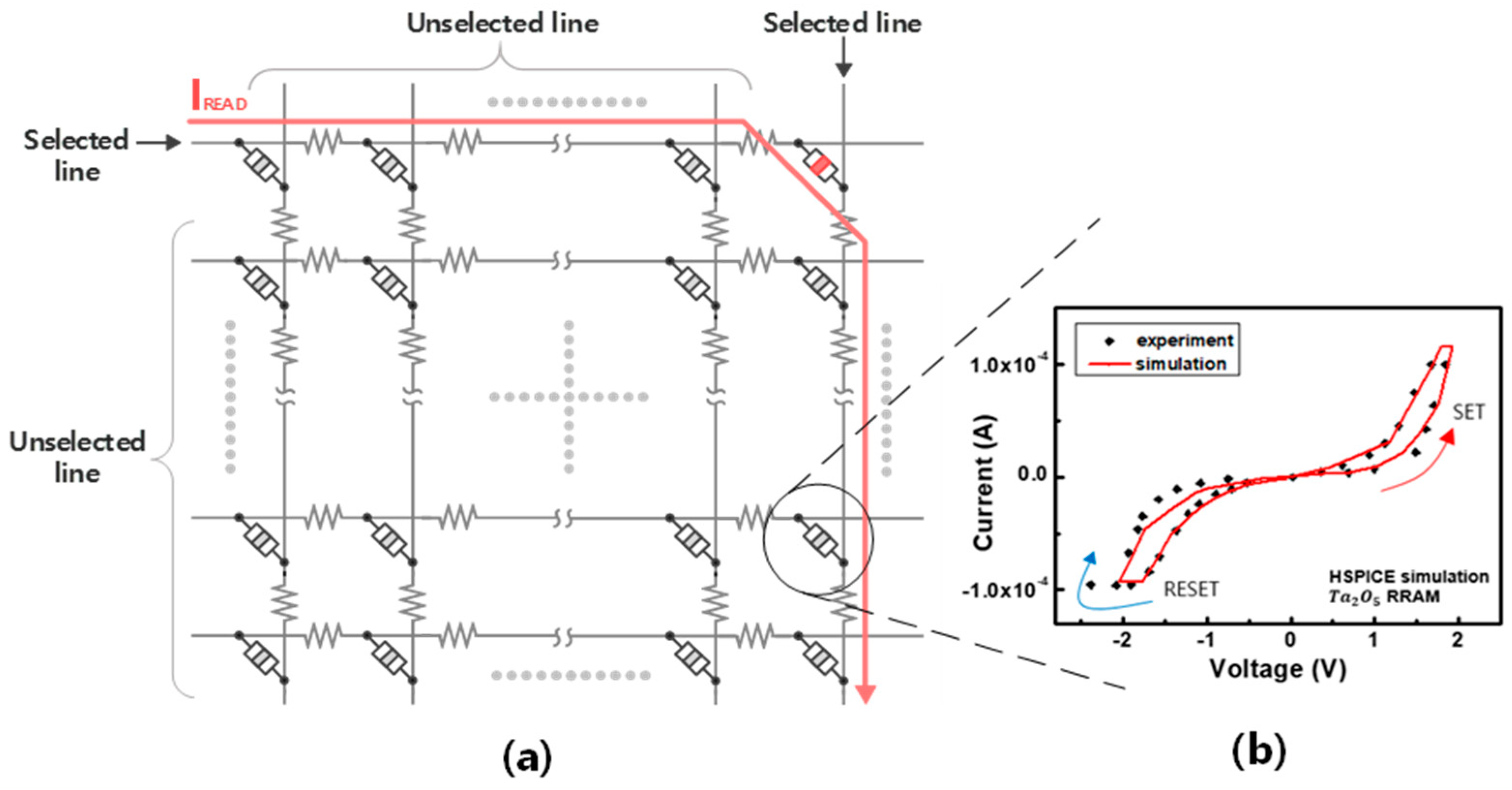
Figure 1. (a) The structure of a nano cross-point array; and (b) the currentvoltage (I-V) characteristics of a T a 2 O 5 memristor implemented in (a). The black diamond-shaped dots show the experimental results for a T a 2 O 5 memristor obtained from [21] and the red line shows the simulated results.
Electronics 09 01446 g001
Figure 2. (a) Resistance change under pulses with various pulsewidths (20, 50, and 100 ns); and (b) resistance distributions of analog memristors in their initial state (black), HRS and LRS states (blue), and gradual transitions induced by various pulses (red).
Electronics 09 01446 g002
Figure 3. (a) A concept of the bank design for a PUF; and (b) a schematic diagram for the practical implementation of the bank design.
Electronics 09 01446 g003
Figure 4. (a) Simplified pm-PUF architecture; (b) row control circuitry; (c) column control circuitry; (d) row decoder circuitry; and (e) column decoder circuitry.
Electronics 09 01446 g004
Figure 5. (a) Sense amplifier block circuitry, where each block has the same circuitry; and (b) voltage distribution quantized into four sections. The voltage indicates the red marked node V m in (a) and each section is allocated to a two-bit response (00, 01, 10, or 11).
Electronics 09 01446 g005
Figure 6. pm-PUF performance evaluation: (a) randomness, the occurrence probability of a “0” and “1” in the responses; (b) diffuseness, the possibility of generating different responses with the same challenge; (c) uniqueness, the possibility of generating different responses among different PUFs; and (d,e) steadiness under (d) temperature and (e) voltage variations.
Electronics 09 01446 g006
Figure 7. (a) The percentage of consumed CRPs; and (b) the number of cycles required according to the increasing number of CRPs.
Electronics 09 01446 g007
Figure 8. Cycle ratios for increasing quantized levels.
Electronics 09 01446 g008
Table 1. Model parameters used in the memristor model.
SymbolValueSymbolValue
a 1 10 5 a 2 10 5
V p 1 (V) V n 1 (V)
A p 3 × 10 6 A n 10 7
α p 7 α n 6
b2 x 0 0.3
Table 2. Comparison of the pm-PUF with other memristor-based PUFs.
[16][36]pm-PUF
Randomness 50%54%50.6%
Uniqueness-38%47.96%
Total CRPsM   ×   NM   ×   N M   × ( N n ) n
Reconfigurablenoyesyes
Multibit-generatingnoyesyes