Article

MFMIS Negative Capacitance FinFET Design for Improving Drive Current

Department of Electrical and Computer Engineering, Sungkyunkwan University, Suwon 16419, Korea
*
Author to whom correspondence should be addressed.
Electronics 2020, 9(9), 1423; https://doi.org/10.3390/electronics9091423
Submission received: 30 July 2020 / Revised: 29 August 2020 / Accepted: 30 August 2020 / Published: 2 September 2020
(This article belongs to the Section Semiconductor Devices)

Abstract

:
The effect of remnant polarization (Pr), coercive electric-field (Ec), and parasitic capacitance of baseline device on the drive current (ION) of a metal-ferroelectric-metal-insulator-semiconductor (MFMIS) negative capacitance FinFET (NC FinFET) was investigated. The internal gate voltage in the MFMIS structure was simulated considering gate leakage current. Using technology computer aided design (TCAD) tool, the device characteristic of 7 nm FinFET was quantitatively estimated, for the purpose of modeling the baseline device of MFMIS NC FinFET. The need for appropriate parasitic capacitance to avoid performance degradation in MFMIS NC FinFET was presented through the internal gate voltage estimation. With an appropriate parasitic capacitance, the effect of Pr and Ec was investigated. In the case of Ec engineering, it is inappropriate to improve the device performance for MFMIS NC FinFET without threshold voltage degradation. Rather than Ec engineering, an adequate Pr value for achieving high ION in MFMIS NC FinFET is suggested.

1. Introduction

The negative capacitance field effect transistor (NCFET) was introduced as one of the steep switching devices [1]. The NCFET enables effectively lowering of the power supply voltage of conventional metal oxide semiconductor field effect transistor (MOSFET) because of its super steep switching feature, i.e., sub-60-mV/decade subthreshold swing at room temperature. Unlike the other steep switching devices (e.g., Tunnel FET [2] and nano-electro-mechanical (NEM) relay [3,4]), the NCFET requires an additional ferroelectric layer in its gate stack. Recent studies demonstrated some conspicuous characteristics of NCFET, e.g., improved subthreshold slope, hysteresis-free behavior, and improved DIBL (drain-induced barrier lowering) effect [5,6,7,8,9,10]. There are several factors which play an important role in determining the performance of NCFET. Those factors include electrical properties, such as coercive electric field (Ec), remnant polarization (Pr), and parasitic capacitance of baseline device without ferroelectric layer. Ec and Pr represent the electrical properties of the ferroelectric layer in NCFET. It is known that a hafnium-based ferroelectric material can have various values of Ec and Pr in a certain range, depending on fabrication conditions or dopants [11,12]. Therefore, the impact of Ec, Pr, and parasitic capacitance on NCFET performance was widely investigated [13,14]. Those studies have shown that the NCFET can improve its subthreshold slope and threshold voltage, by taking appropriate values of Ec, Pr, and parasitic capacitance. Additionally, the gate stack structure in NCFET affects the device performance of NCFET. As a gate stack structure for NCFET, a metal-ferroelectric-metal-insulator-semiconductor (MFMIS) structure was suggested. It was expected that the intermediate metal layer in the MFMIS structure can act as an equipotential layer that alleviates multi-domain effects, so that it generates a higher voltage gain than in a metal-ferroelectric-insulator-semiconductor (MFIS) structure [15,16]. However, Khan et al. [17] showed that, if there exists a leakage current in the MFMIS structure, it is impossible for the polarization of ferroelectric material to stably exist in the negative capacitance (NC) region (i.e., where dP/dV < 0). This is because the polarization of ferroelectric material slips toward either positive or negative Pr, so that a stabilized voltage gain cannot be expected. There is little study of the impact of those parameters on the device performance of MFMIS NCFET (which is affected by the leakage of intermediate metal). To benefit the performance improvement in MFMIS NCFET, the impact of Ec, Pr, and parasitic capacitance should be investigated. In this work, the impact of Ec, Pr, and parasitic capacitance on MFMIS NC FinFET was investigated through the framework of Khan and 7 nm technology node fin-shaped field effect transistor (FinFET). In addition, we suggest how to design the MFMIS NC FinFET to obtain better device performance.

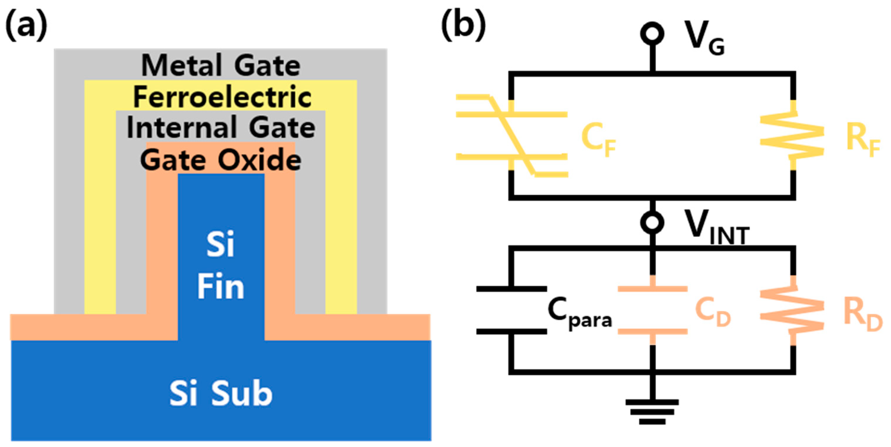
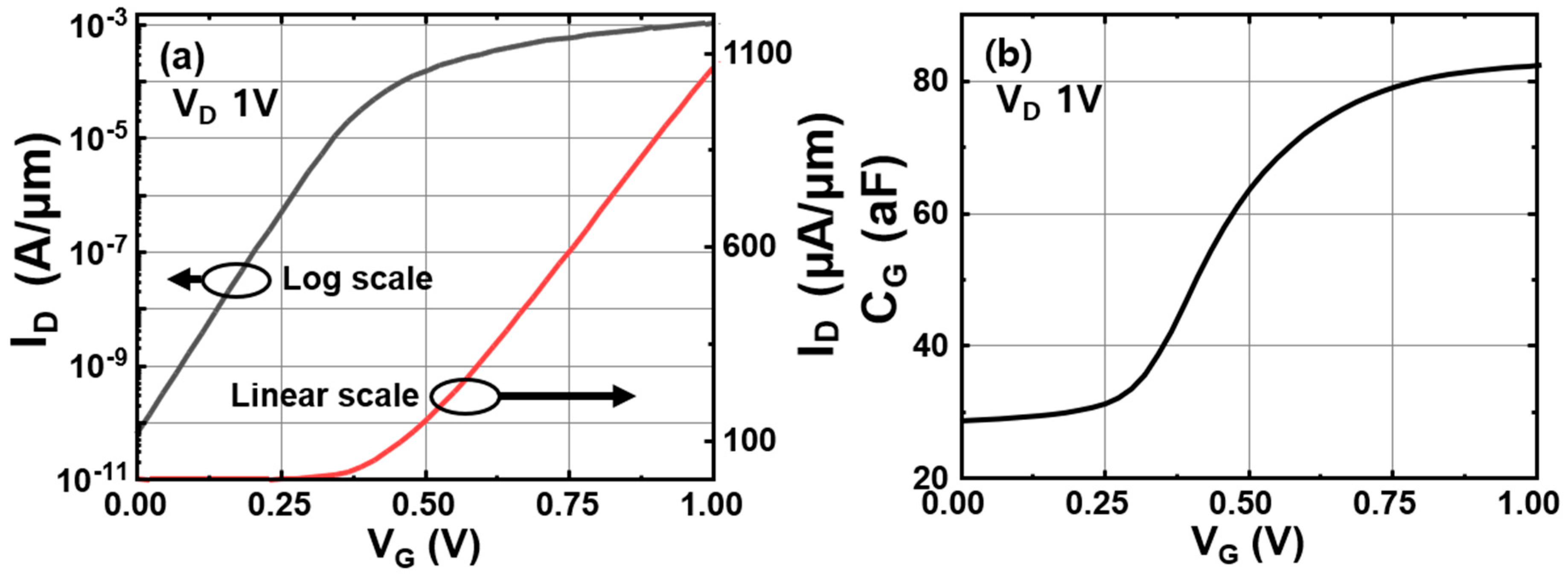
2. Simulation Method for MFMIS NC FinFET

The MFMIS structure for NCFET was used in this work (see Figure 1a). Due to the leakage current through the internal gate, the ferroelectric layer cannot stay in the negative capacitance region (i.e., negative slope region in polarization-vs.-electric field plot of ferroelectric material), and thereby, the MFMIS NCFET cannot be expected to benefit the stable voltage amplification of the ferroelectric layer. In order to take advantage of using the voltage amplification of the ferroelectric layer in MFMIS NCFET, the dynamic response should be considered. From the perspective of time-dependency, we have used the framework of [17] to estimate the voltage amplification in MFMIS NCFET. In reference [17], the metal-ferroelectric-metal-insulator-metal (MFMIM) structure was modeled as the series-connected circuit network (see Figure 1b). The ferroelectric and dielectric thin film can be modeled as the parallel connection of the capacitor and resistor, and the intermetal layer was modeled as the internal node because the intermetal layer acts as the equipotential surface between the ferroelectric and dielectric film. The polarization-vs.-electric-field behavior of ferroelectric material is analytically described with the Landau-Khalatnikov (LK) Equation (1) as below.
V F = T F · ( α · P F + β · P F 3 ) ,
where TF indicates the thickness of ferroelectric layer, and the coefficients (i.e., α and β) are defined as below.
α = 3 3 2 · ( E c / P r )       ,     β = 3 3 2 · ( E c / P r 3 )
Applying the Kirchhoff’s current law at the internal metal of the series network, we can derive the equation below.
d Q F d t = C D d V G d t + V G R D ( 1 R F + 1 R D ) ( α Q F + β Q F 3 ) 1 + C D ( α + 3 β Q F 2 )   ,
where RF, RD are computed as Vapp/(JL × A), where JL is the leakage current that is approximately 10−2 A/cm2 for an applied bias of 1 V [18]. The equation shows the amount of charge in the ferroelectric layer over time. Thus, applying a triangular pulse, the amount of charge in the ferroelectric layer can be estimated, and thereby, it turned out that the MFMIM structure can show the voltage amplification across the ferroelectric layer. Note that the equation is derived from the MFMIM structure, but it is applicable to MFMIS NCFET [19].
Although the MFMIS NCFET can use the negative slope region of ferroelectric layer, the performance degradation of the MFMIS NCFET was expected. The work function engineering was suggested to prevent the performance degradation as well as to enhance the on-state drive current of NCFET [19]. Using metal materials with two different work function values to wrap around the ferroelectric layer, the S-curves in polarization versus voltage plot can be shifted along the voltage axis. The voltage shift can put the ferroelectric into the negative capacitance state (i.e., a smaller amount of VG can put the ferroelectric into the negative capacitance state). In this simulation work, 0.2 V of Voffset is applied through the work function engineering between two metal layers (see Figure 2a). It is noteworthy that the ID-vs.-VG and CG-vs.-VG of baseline FinFET without MFM layer are estimated using Sentaurus TCAD tool (see Figure 3). The FinFET is modeled in accordance with 7 nm technology of IRDS 2017 roadmap [20]. The physical device dimensions of the FinFET are shown in Table 1. With the estimated ID-vs.-VG and CG-vs.-VG of baseline FinFET, and the Equation (3), the ID-vs.-VG of MFMIS NC FinFET was estimated. In this work, the capacitance condition was well satisfied in all VG sweep regions [1], so that there is no hysteresis in the ID-vs.-VG of MFMIS NC FinFET.

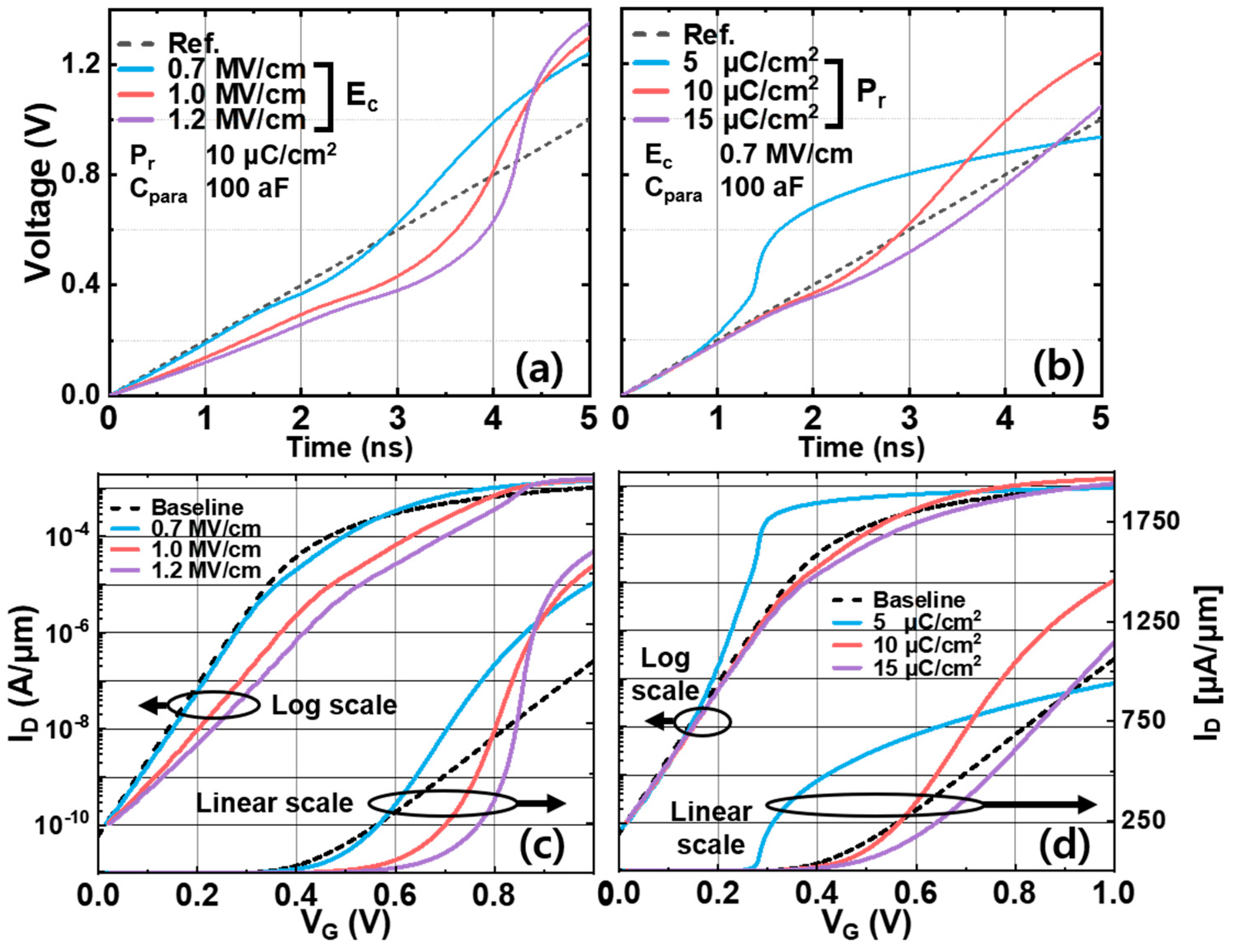
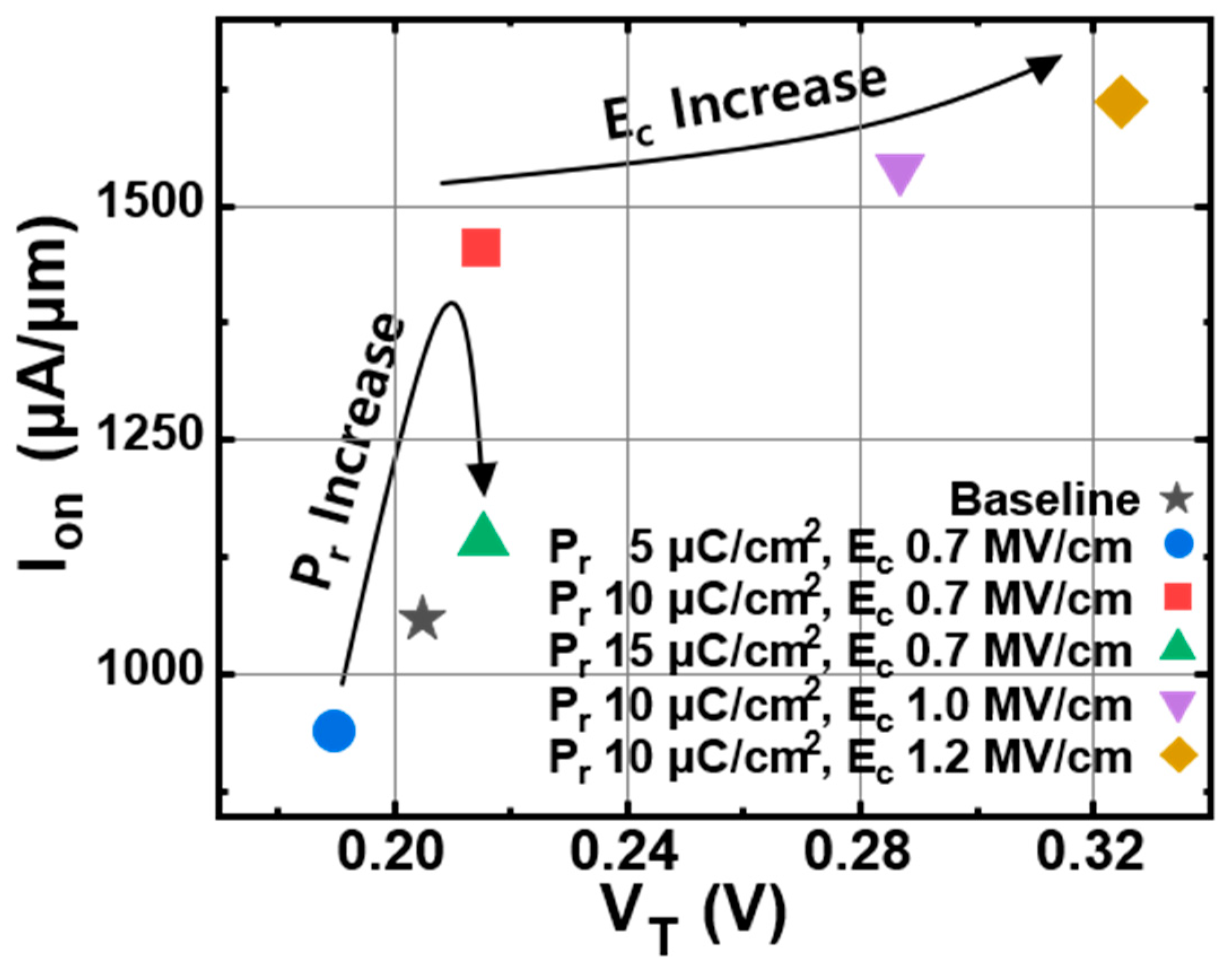
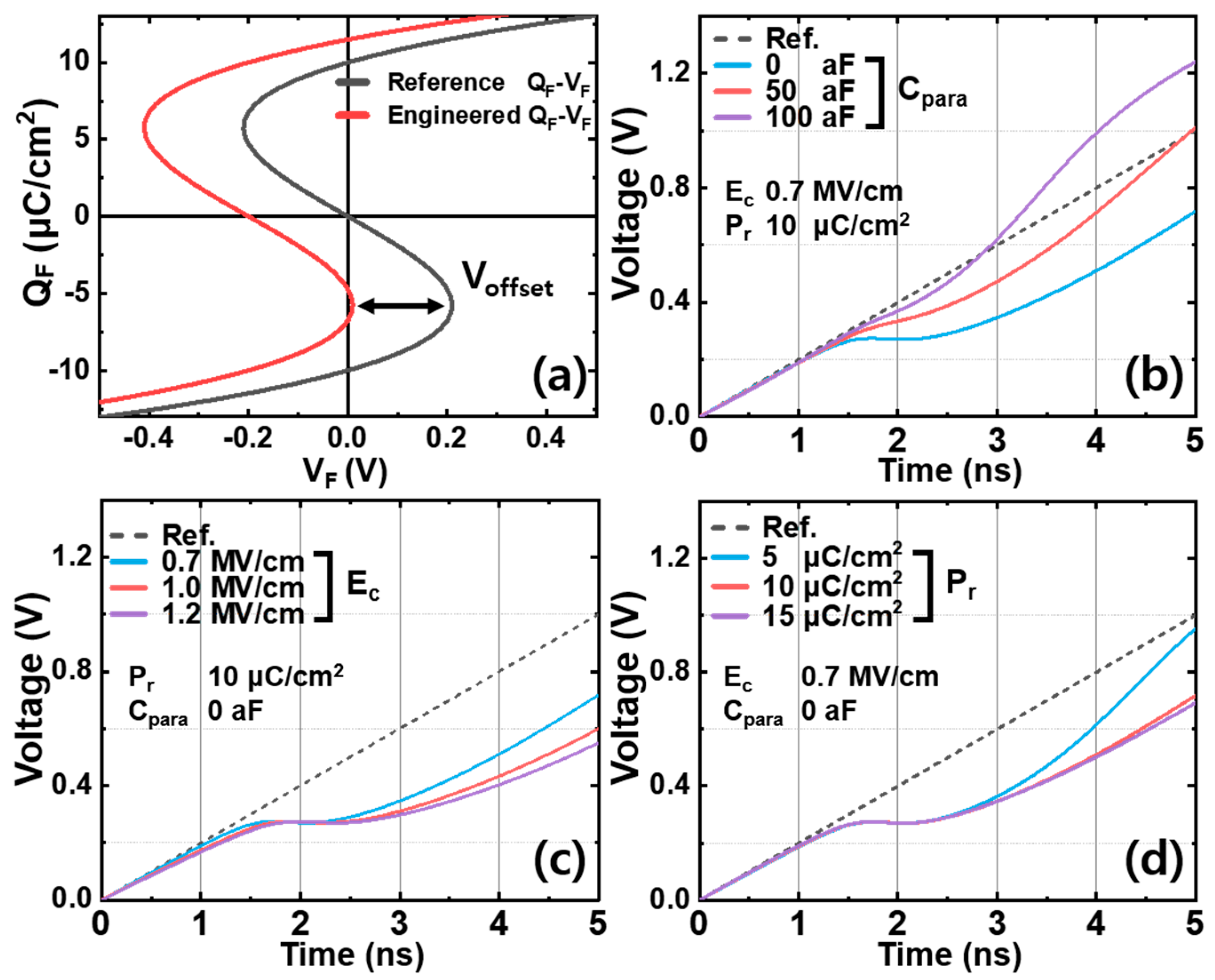
3. Effect of Ec, Pr, and Parasitic Capacitance on MFMIS NC FinFET

Using (1) 100 MHz 1 V triangular pulses, (2) the parameter of hafnium oxide ferroelectric material, and (3) CG-vs.-VG of baseline device, we can find out the voltage-vs.-time characteristic of MFMIS NC FinFET. Note that Ec and Pr used for the S-curve in Figure 2a was 0.7 MV/cm and 10 μC/cm2, respectively [12,13,14]. The S-curve of ferroelectric material (in which the work function is engineered) is shown in Figure 2a. We used the 100 MHz frequency because if the frequency of sweeping VG is faster than the “effective time constant” [17], the impact of the leakage current should be neglected.
The impact of varied Ec and Pr of ferroelectric material is shown in Figure 2c,d. As shown in the figures, the internal voltage decreased and was lower than the reference voltage over the whole time. The internal voltage decreases more with increasing Ec. In the case of decreasing Pr, the internal voltage increases but is still lower than the reference voltage over the whole time. The reason for the internal voltage lowering comes from the fact that CG in the baseline FinFET increases at about 0.3 V (see Figure 3b) due to the inversion layer, and thereby, the internal amplification deteriorates. In this case, an appropriate parasitic capacitance can alleviate the internal voltage lowering, and therefore, it induces a proper voltage amplification in MFMIS structure (see Figure 2b). Total device capacitance (CTOT) can be calculated as (CG + Cpara). In the case of 100 aF of parasitic capacitance, VINT of ≈1.2 V can be implemented by applying a VG of 1 V. By applying 100 aF of parasitic capacitance to obtain a proper voltage amplification, the impact of Ec and Pr was investigated again. First, increasing Ec makes the amount of voltage amplification (at 1 V of reference voltage) become higher (see Figure 4a). However, at a low reference voltage, the lowering of internal voltage becomes severe. This is because a higher Ec needs additional voltage to put ferroelectric material into the negative slope region. In the case of higher Ec, the lowering of internal voltage can be compensated using different metal (which makes Voffset more than 0.2 V) [8].
When Pr is increased, the reference voltage (at which the internal voltage is amplified) is pushed to a higher voltage (see Figure 4b). Low Pr (i.e., 5 μC/cm2) can derive the voltage amplification at a much lower reference voltage. However, the internal voltage at a high reference voltage will be degraded. Additionally, even if Pr becomes lower, it is hard to expect performance enhancement at the deep subthreshold region. In the case of high Pr (i.e., 15 μC/cm2), the internal voltage loses the voltage amplification in all regions of the reference voltages. Using the internal voltages of various conditions, ID-vs.-VG of NC FinFETs were estimated (see Figure 4c,d). In the ID-vs.-VG of NC FinFETs, the on-state drive current (ION) and threshold voltage (VT) were extracted (see Figure 5). Note that VT was extracted at the constant current of 100 nA/um. Higher Ec enables the MFMIS NC FinFET to achieve the highest ION, but, at the same time, it increases VT significantly. If Pr is in-between 5 μC/cm2 and 10 μC/cm2, ION and VT have a trade-off relationship to each other. However, the trade-off is not found in the case of 15 μC/cm2. Even using a low Pr in MFMIS NC FinFET, a significant improvement in VT is hard to expect.

4. Conclusions

The impact of Ec, Pr, and parasitic capacitance on the performance of MFMIS NC FinFET was investigated. To find out the voltage of intermediate metal in the MFMIS structure, Landau-Khalatnikov model with the gate leakage current was used. Investigating the effect of parasitic capacitance on the MFMIS structure, the parasitic capacitance can be the key knob to control the internal voltage. With 100 aF of parasitic capacitance, Ec and Pr in ferroelectric material were varied between 5–15 μC/cm2 and 0.7–1.2 MV/cm, respectively. In order to design MFMIS NC FinFET to achieve high drive current, Ec of 1.2 MV/cm can induce the highest drive current (i.e., 1.5 times higher drive current than in baseline device). However, the threshold voltage of the NC FinFET was increased (by ≈0.12 V) than that of baseline device. On the other hand, the NC FinFET with an appropriate value of Pr (i.e., 10 μC/cm2) can achieve 1.4 times higher drive current than baseline device with little VT degradation.

Author Contributions

Conceptualization, J.M. and C.S.; methodology, J.M.; software, J.M.; validation, J.M. and C.S.; formal analysis, J.M.; investigation, J.M.; resources, J.M.; data curation, J.M. and C.S.; writing—original draft preparation, J.M.; writing—review and editing, C.S.; visualization, J.M.; supervision, C.S.; project administration, C.S.; funding acquisition, C.S. All authors have read and agreed to the published version of the manuscript.

Funding

This study was supported by the National Research Foundation of Korea (NRF) through a grant funded by the Korean government (MSIP; No. 2020R1A2C1009063, 2020M3F3A2A01081672, and 2020M3F3A2A02082473). Additionally, this work was supported by the Future Semiconductor Device Technology Development Program (10067746) funded by the Ministry of Trade, Industry & Energy (MOTIE), and the Korea Semiconductor Research Consortium (KSRC). The EDA Tool was supported by the IC Design Education Center.

Conflicts of Interest

The authors declare no conflict of interest.

References

  1. Salahuddin, S.; Datta, S. Use of negative capacitance to provide voltage amplification for low power nanoscale devices. Nano Lett. 2008, 8, 405. [Google Scholar] [CrossRef] [PubMed]
  2. Choi, W.Y.; Park, B.; Lee, J.D.; Liu, T.K. Tunneling Field-Effect Transistors (TFETs) With Subthreshold Swing (SS) Less Than 60 mV/dec. IEEE Electron Device Lett. 2007, 28, 743. [Google Scholar] [CrossRef]
  3. Choe, K.; Shin, C. Adjusting the Operating Voltage of an Nanoelectromechanical Relay Using Negative Capacitance. IEEE Trans. Electron Devices 2017, 64, 5270. [Google Scholar] [CrossRef]
  4. Nathanael, R.; Pott, V.; Kam, H.; Jeon, J.; Liu, T.K. 4-terminal relay technology for complementary logic. In Proceedings of the 2009 IEEE International Electron Devices Meeting (IEDM), Baltimore, MD, USA, 7–9 December 2009. [Google Scholar]
  5. Jo, J.; Choi, W.Y.; Park, J.-D.; Shim, J.W.; Yu, H.-Y.; Shin, C. Negative capacitance in organic/ferroelectric capacitor to implement steep switching MOS devices. Nano Lett. 2015, 15, 4553. [Google Scholar] [CrossRef] [PubMed]
  6. Jo, J.; Shin, C. Negative capacitance field effect transistor with hysteresis-free sub-60-mV/decade switching. IEEE Electron Device Lett. 2016, 37, 245. [Google Scholar] [CrossRef]
  7. Li, K.-S.; Chen, P.-G.; Lai, T.-Y.; Lin, C.-H.; Cheng, C.-C.; Chen, C.-C.; Wei, Y.-J.; Hou, Y.-F.; Liao, M.-H.; Lee, M.-H.; et al. Sub-60mV-swing negative-capacitance FinFET without hysteresis. In Proceedings of the 2015 IEEE International Electron Devices Meeting (IEDM), Washington, DC, USA, 7–9 December 2015. [Google Scholar]
  8. Zhou, H.; Kwon, D.; Sachid, A.B.; Liao, Y.; Chatterjee, K.; Tan, A.J.; Yadav, A.K.; Hu, C.; Salahuddin, S. Negative Capacitance, n-Channel, Si FinFETs: Bi-directional Sub-60 mV/dec, Negative DIBL, Negative Differential Resistance and Improved Short Channel Effect. In Proceedings of the 2018 IEEE Symposium on VLSI Technology, Honolulu, HI, USA, 18–22 June 2018; p. 53. [Google Scholar]
  9. Kwon, D.; Chatterjee, K.; Tan, A.J.; Yadav, A.K.; Zhou, H.; Sachid, A.B.; Dos Reis, R.; Hu, C.; Salahuddin, S. Improved Subthreshold Swing and Short Channel Effect in FDSOI n-Channel Negative Capacitance Field Effect Transistors. IEEE Electron Device Lett. 2018, 39, 300. [Google Scholar] [CrossRef]
  10. Shin, J.; Shin, C. Experimental observation of zero DIBL in short-channel hysteresis-free ferroelectric-gated FinFET. Solid State. Electron. 2018, 153, 12. [Google Scholar] [CrossRef]
  11. Kim, T.; Jeon, S. Pulse switching study on the HfZrO ferroelectric films with high pressure annealing. IEEE Trans. Electron Devices 2018, 65, 1771. [Google Scholar] [CrossRef]
  12. Kobayashi, M.; Hiramoto, T. Device design guideline for steep slope ferroelectric FET using negative capacitance in sub-0.2V operation: Operation speed, material requirement and energy efficiency. In Proceedings of the 2015 Symposium on VLSI Technology (VLSI Technology), Kyoto, Japan, 16–18 June 2015; p. T212. [Google Scholar]
  13. Khandelwal, S.; Duarte, J.; Khan, A.; Salahuddin, S.; Hu, C. Impact of parasitic capacitance and ferroelectric parameters on negative capacitance FinFET characteristics. IEEE Electron Device Lett. 2017, 38, 142. [Google Scholar] [CrossRef]
  14. Lin, C.; Khan, A.; Salahuddin, S.; Hu, C. Effects of the Variation of Ferroelectric Properties on Negative Capacitance FET Characteristics. IEEE Trans. Electron Devices 2016, 63, 2197. [Google Scholar] [CrossRef]
  15. Saha, A.K.; Sharma, P.; Dabo, I.; Datta, S.; Gupta, S.K. Ferroelectric transistor model based on self-consistent solution of 2D Poisson’s, non-equilibrium Green’s function and multi-domain Landau Khalatnikov equations. In Proceedings of the 2017 IEEE International Electron Devices Meeting (IEDM), San Francisco, CA, USA, 2–6 December 2017. [Google Scholar]
  16. Pahwa, G.; Agarwal, A.; Chauhan, Y.S. Numerical Investigation of Short-Channel Effects in Negative Capacitance MFIS and MFMIS Transistors: Above-Threshold Behavior. IEEE Trans. Electron Devices 2019, 66, 1591. [Google Scholar] [CrossRef]
  17. Khan, A.I.; Radhakrishna, U.; Chatterjee, K.; Salahuddin, S.; Antoniadis, D.A. Negative Capacitance Behavior in a Leaky Ferroelectric. IEEE Trans. Electron Devices 2016, 63, 4416. [Google Scholar] [CrossRef]
  18. Ando, T.; Sathaye, N.D.; Murali, K.V.R.M.; Cartier, E.A. On the Electron and Hole Tunneling in a HfO2 Gate Stack with Extreme Interfacial-Layer Scaling. IEEE Electron Device Lett. 2011, 32, 865. [Google Scholar] [CrossRef]
  19. Khan, A.I.; Radhakrishna, U.; Salahuddin, S.; Antoniadis, D. Work Function Engineering for Performance Improvement in Leaky Negative Capacitance FETs. IEEE Electron Device Lett. 2017, 38, 1335. [Google Scholar] [CrossRef]
  20. The International Roadmap for Devices and Systems (IRDS 2017). Available online: https://irds.ieee.org/roadmap-2017 (accessed on 1 August 2019).
Figure 1. (a) Cross-sectional schematic of MFMIS NC FinFET. (b) Circuit configuration of MFMIM structure. CD, CF, Cpara, RF, RD indicates the capacitance of dielectric, ferroelectric layer, and parasitic capacitance; and the resistance of the dielectric and ferroelectric layer, respectively. VG and VINT represents the gate voltage and internal metal voltage, respectively.
Electronics 09 01423 g001
Figure 2. (a) Two S-curves are drawn in polarization versus voltage plot. The red-colored one is the S-curve with work function engineering. The black-colored one is the reference S-curve, for comparison. Note that Pr and Ec of the reference S-curve are 10 μC/cm2 and 0.7 MV/cm, respectively. VINT-vs.-time for (b) various parasitic capacitances, (c) Ec, and (d) Pr. Note that the reference line (black-colored dotted line) indicates the 100 MHz 1 V triangular pulse.
Electronics 09 01423 g002
Figure 3. (a) Estimated current-vs.-voltage (ID-vs.-VG) of baseline FinFET in log (left) and linear (right) scale. (b) Estimated capacitance-vs.-voltage (CG-vs.-VG) of baseline FinFET.
Electronics 09 01423 g003
Figure 4. VINT-vs.-time for a few Ec (a) and Pr (b). The black-colored dotted reference line indicates the 100 MHz 1 V triangular pulse. The estimated drain current-vs.-gate voltage (ID-vs.-VG) of baseline FinFET (see the black-colored solid line) and MFMIS NC FinFET (see the blue/red/purple-colored solid lines) for a few Ec (c) and Pr (d).
Electronics 09 01423 g004
Figure 5. Scatter plot of extracted ION and VT of various MFMIS NC FinFETs.
Electronics 09 01423 g005
Table 1. The important device parameters for MFMIS NC FinFET.
Device ParameterQuantityDevice ParameterQuantity
Gate Length, LG18 nmOxide Thickness 1, TOX3 nm
Spacer Thickness, LSP7 nmChannel Doping, NSP1015 cm−3
Fin Height, HFin50 nmSource/Drain Doping, NSD1020 cm−3
Fin Width, WFin7 nmFerroelectric Thickness, TF3 nm
1 Hafnium oxide was used as the gate oxide.

