High Pressure Processing of Ion Implanted GaN

 , , , , ,
Abstract
:1. Introduction
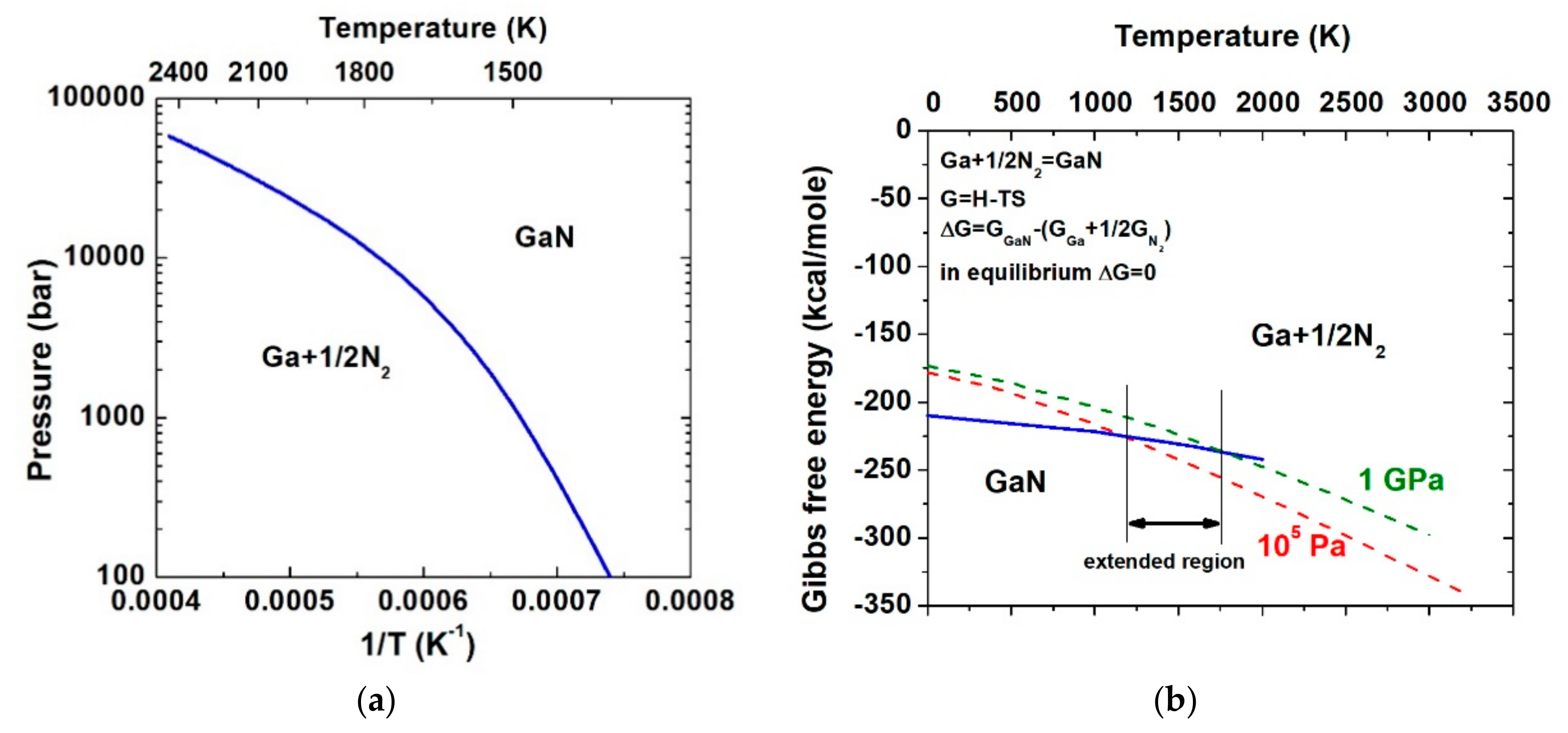
2. Thermodynamic Basics
3. Ultra-High-Pressure Annealing Process
4. P-Type GaN by Mg Implantation
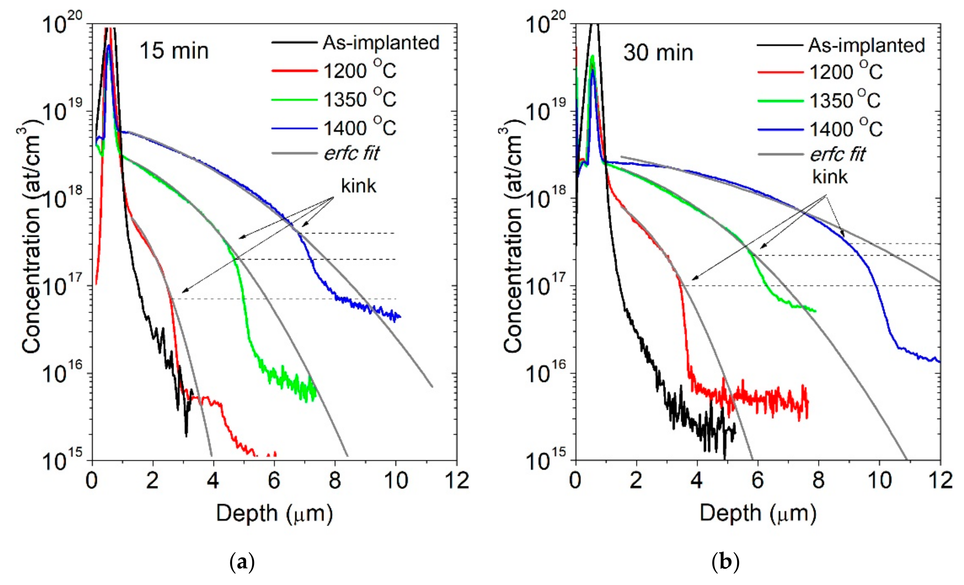
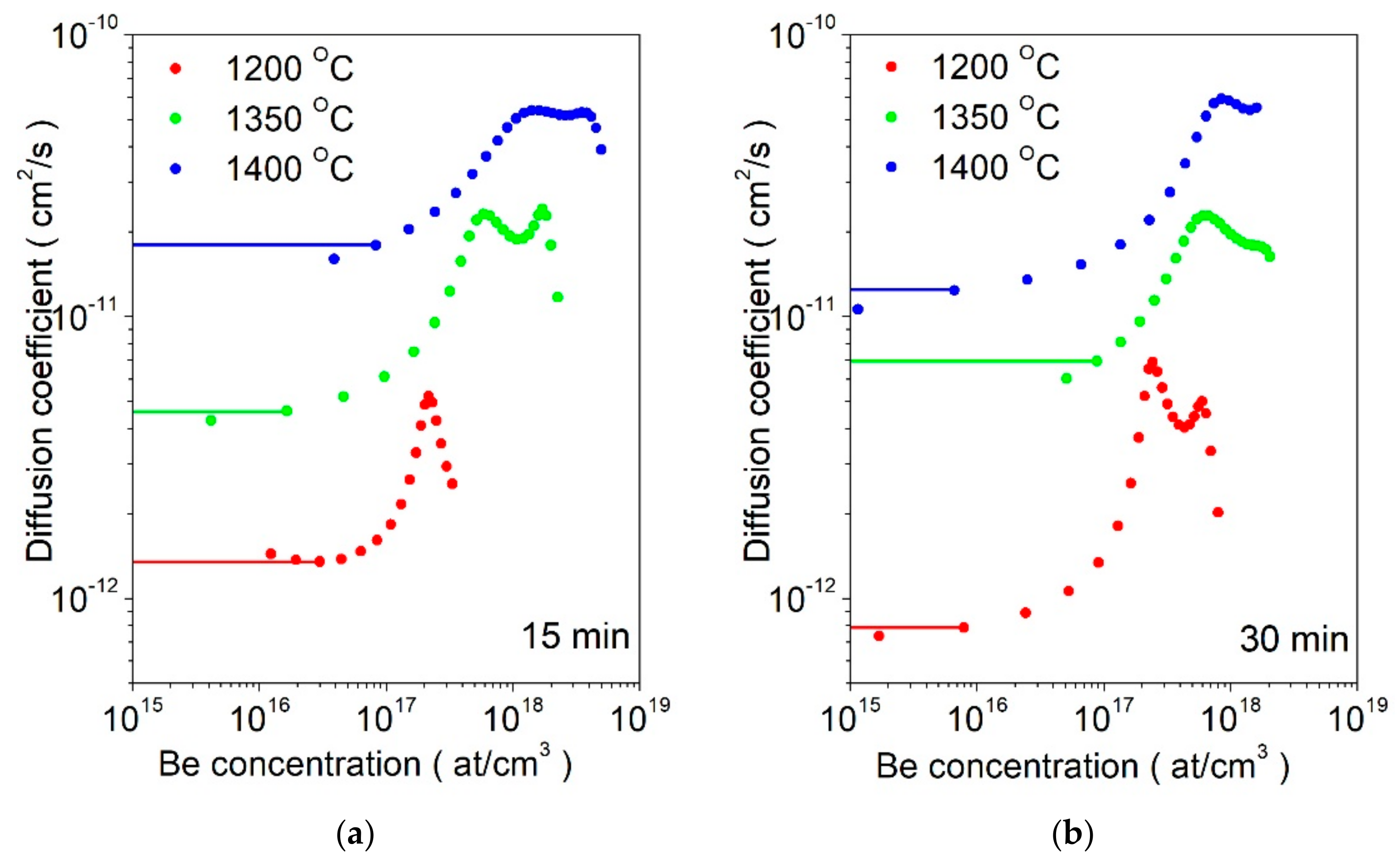
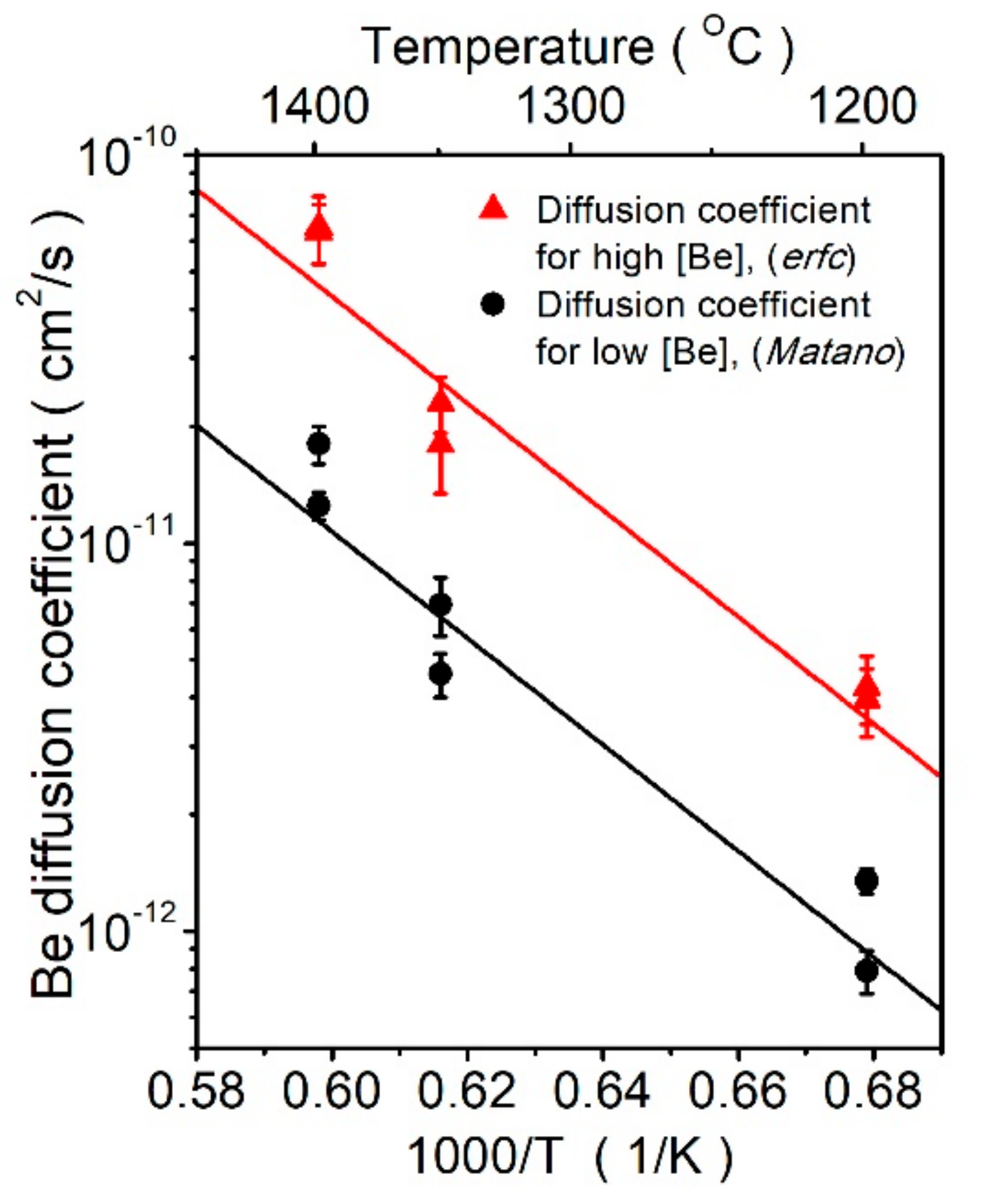
5. Diffusion Mechanism of Beryllium in GaN—Case Study
6. Summary
Author Contributions
Funding
Acknowledgments
Conflicts of Interest
References
- Shibata, D.; Kajitani, R.; Ogawa, M.; Tanaka, K.; Tamura, S.; Hatsuda, T.; Ishida, M.; Ueda, T.T. 1.7 kV/1.0 mΩcm2 normally-off vertical GaN transistor on GaN substrate with regrown p-GaN/AlGaN/GaN semipolar gate structure. In Proceedings of the IEEE International Electron Devices Meeting (IEDM16), San Francisco, CA, USA, 3–7 December 2016; p. 248. [Google Scholar]
- Takashima, S. Demonstration of vertical GaN planar MOSFET fabricated by all ionimplantation process. In Proceedings of the Invited Lecture during 9th Asia-Pacific Workshop on Widegap Semiconductors (APWS2019), Okinawa, Japan, 10–15 November 2019. [Google Scholar]
- Zolper, J.C. Ion implantation in group III-nitride semiconductors: A tool for doping and defect studies. J. Cryst. Growth 1997, 178, 157–167. [Google Scholar] [CrossRef]
- Irokawa, Y.; Fujishima, O.; Kachi, T.; Nakano, Y. Electrical activation characteristics of silicon-implanted GaN. J. Appl. Phys. 2005, 97, 083505. [Google Scholar] [CrossRef]
- Greenlee, J.D.; Feigelson, B.N.; Anderson, T.J.; Tadjer, M.J.; Hite, J.K.; Mastro, M.A.; Eddy, C.R.J.; Hobart, K.D.; Kub, F.J. Multicycle rapid thermal annealing optimization of Mg-implanted GaN: Evolution of surface, optical, and structural properties. J. Appl. Phys. 2014, 116, 063502. [Google Scholar] [CrossRef]
- Oikawa, T.; Saijo, Y.; Kato, S.; Mishima, T.; Nakamura, T. Formation of definite GaN p–n junction by Mg-ion implantation to n−-GaN epitaxial layers grown on a high-quality free-standing GaN substrate. Nucl. Instrum. Methods Phys. Res. Sect. B 2015, 365, 168–170. [Google Scholar] [CrossRef]
- Pearton, S.J.; Vartuli, C.B.; Zolper, J.C.; Yuan, C.; Stall, R.A. Ion implantation doping and isolation of GaN. Appl. Phys. Lett. 1995, 67, 1435. [Google Scholar] [CrossRef]
- Uedono, A.; Takashima, S.; Edo, M.; Ueno, K.; Matsuyama, H.; Kudo, H.; Naramoto, H.; Ishibashi, S. Vacancy-type defects and their annealing behaviors in Mg-implanted GaN studied by a monoenergetic positron beam. Phys. Status Solidi B 2015, 252, 2794–2801. [Google Scholar] [CrossRef]
- Karpiński, J.; Porowski, S. High pressure thermodynamics of GaN. J. Cryst. Growth 1984, 66, 11–20. [Google Scholar] [CrossRef]
- Ehrentraut, D.; Bockowski, M. Handbook of Crystal Growth Second Edition: Bulk Crystal Growth: Basic Techniques, and Growth Mechanisms and Dynamics; Rudolph, P., Ed.; Elsevier: Amsterdam, The Netherlands, 2015; pp. 577–619. [Google Scholar]
- Grzegory, I.; Bockowski, M.; Porowski, S. Bulk Crystal Growth of Electronic, Optical and Optoelectronic Materials; Capper, P., Ed.; Wiley & Sons: Hoboken, NJ, USA, 2005; p. 173. [Google Scholar]
- Ben Sedrine, N.; Rodrigues, J.; Cardoso, J.; Nd Faye, D.; Fialho, M.; Magalhães, S.; Martins, A.F.; Neves, A.J.; Alves, E.; Bockowski, M.; et al. Optical investigations of europium ion implanted in nitride-based diode structures. Surf. Coat. Technol. 2018, 355, 40–44. [Google Scholar] [CrossRef]
- Ben Sedrine, N.; Rodrigues, J.C.; Nd Faye, D.; Neves, A.J.; Alves, E.; Bockowski, M.; Hoffmann, V.; Weyers, M.; Lorenz, K.; Correia, M.R.; et al. Eu-Doped AlGaN/GaN Superlattice-Based Diode Structure for Red Lighting: Excitation Mechanisms and Active Sites. ACS Appl. Nano Mater. 2018, 1, 3845–3858. [Google Scholar] [CrossRef]
- Singh, A.K.; O’Donnell, K.P.; Edwards, P.R.; Lorenz, K.; Kappers, M.J.; Bockowski, M. Hysteretic photochromic switching of Eu-Mg defects in GaN links the shallow transient and deep ground states of the Mg acceptor. Sci. Rep. 2017, 7, 41982. [Google Scholar] [CrossRef] [Green Version]
- Singh, A.K.; O’Donnell, K.P.; Edwards, P.R.; Cameron, D.; Lorenz, K.; Kappers, M.J.; Bockowski, M.; Yamaga, M.; Prakash, R. Luminescence of Eu3+ in GaN (Mg, Eu): Transitions from the 5D1 level. Appl. Phys. Lett. 2017, 111, 241105. [Google Scholar] [CrossRef] [Green Version]
- Lorenz, K.; Miranda, S.M.C.; Alves, E.; Roqan, I.S.; O’Donnell, K.P.; Bockowski, M. High pressure annealing of Europium implanted GaN. In Proceedings of the SPIE, San Francisco, CA, USA, 21–26 January 2012; Volume 8262. UNSP 82620C. [Google Scholar]
- Smedskjaer, M.M.; Rzoska, S.J.; Bockowski, M.; Mauro, J.C. Mixed alkaline earth effect in the compressibility of aluminosilicate glasses. J. Chem. Phys. 2014, 140, 054511. [Google Scholar] [CrossRef] [PubMed]
- Svenson, M.N.; Bechgaard, T.K.; Fuglsang, S.D.; Pedersen, R.H.; Tjell, A.Ø.; Østergaard, M.B.; Youngman, R.E.; Mauro, J.C.; Rzoska, S.J.; Bockowski, M.; et al. Composition-Structure-Property Relations of Compressed Borosilicate Glasses. Phys. Rev. Appl. 2014, 2, 024006. [Google Scholar] [CrossRef]
- Smedskjaer, M.M.; Bauchy, M.; Mauro, J.C.; Rzoska, S.J.; Bockowski, M. Unique effects of thermal and pressure histories on glass hardness: Structural and topological origin. J. Chem. Phys. 2015, 143, 164505. [Google Scholar] [CrossRef] [PubMed]
- Svenson, M.N.; Guerette, M.; Huang, L.; Lönnroth, N.; Mauro, J.C.; Rzoska, S.J.; Bockowski, M.; Smedskjaer, M.M. Universal behavior of changes in elastic moduli of hot compressed oxide glasses. Chem. Phys. Lett. 2016, 651, 88–91. [Google Scholar] [CrossRef] [Green Version]
- Østergaard, M.B.; Petersen, R.R.; König, J.; Bockowski, M.; Yue, Y.J. Foam glass obtained through high-pressure sintering. Am. Ceram. Soc. 2018, 101, 3917–3923. [Google Scholar] [CrossRef]
- Bockowski, M.; Iwinska, M.; Amilusik, M.; Fijalkowski, M.; Lucznik, B.; Sochacki, T. Challenges and future perspectives in HVPE-GaN growth on ammonothermal GaN seeds. Semicond. Sci. Technol. 2016, 31, 093002. [Google Scholar] [CrossRef]
- Nakano, Y.; Jimbo, T. Co-implantation of Si+N into GaN for n-type doping. J. Appl. Phys. 2002, 92, 3815. [Google Scholar] [CrossRef]
- Sakurai, H.; Omori, M.; Yamada, S.; Furukawa, Y.; Suzuki, H.; Narita, T.; Kataoka, K.; Horita, M.; Boćkowski, M.; Suda, J.; et al. Highly effective activation of Mg-implanted p-type GaN by ultra-high-pressure annealing. Appl. Phys. Lett. 2019, 115, 142104. [Google Scholar]
- Narita, T.; Sakurai, H.; Bockowski, M.; Kataoka, K.; Suda, J.; Kachi, T. Electric-field-induced simultaneous diffusion of Mg and H in Mg-doped GaN prepared using ultra-high-pressure annealing. Appl. Phys. Express 2019, 12, 111005. [Google Scholar] [CrossRef]
- Iwata, K.; Sakurai, H.; Arai, S.; Nakashima, T.; Narita, T.; Kataoka, K.; Bockowski, M.; Nagao, M.; Suda, J.; Kachi, T.; et al. Defect evolution in Mg ions implanted GaN upon high temperature and ultrahigh N2 partial pressure annealing: Transmission electron microscopy analysis. Appl. Phys. 2020, 127, 105106. [Google Scholar] [CrossRef]
- Wang, Y.; Huynh, K.; Liao, M.E.; Yu, H.-M.; Bai, T.; Tweedie, J.; Breckenridge, M.H.; Collazo, R.; Sitar, Z.; Bockowski, M.; et al. Strain Recovery and Defect Characterization in Mg-Implanted Homoepitaxial GaN on High-Quality GaN Substrates. Phys. Status Solidi B 2020, 257, 1900705. [Google Scholar] [CrossRef]
- Horita, M.; Takashima, S.; Tanaka, R.; Matsuyama, H.; Ueno, K.; Edo, M.; Takanashi, T.; Shimizu, M.; Suda, J. Hall-effect measurements of metalorganic vapor-phase epitaxy-grown p-type homoepitaxial GaN layers with various Mg concentrations. Jpn. J. Appl. Phys. 2017, 56, 031001. [Google Scholar] [CrossRef]
- Kumar, A.; Uzuhashi, J.; Ohkubo, T.; Tanaka, R.; Takashima, S.; Edo, M.; Hono, K. Atomic-scale quantitative analysis of implanted Mg in annealed GaN layers on free-standing GaN substrates. J. Appl. Phys. 2019, 126, 235704. [Google Scholar] [CrossRef]
- Zajac, M.; Kucharski, R.; Grabianska, K.; Gwardys-Bak, A.; Puchalski, A.; Wasik, D.; Litwin-Staszewska, E.; Piotrzkowski, R.; Domagala, J.Z.; Bockowski, M. Basic ammonothermal growth of Gallium Nitride–State of the art, challenges, perspectives. Prog. Cryst. Growth Charact. Mater. 2018, 64, 63–74. [Google Scholar] [CrossRef]
- Matano, C. On the Relation between Diffusion-Coefficients and Concentrations of Solid Metals. Jpn. J. Phys 1932, 8, 109. [Google Scholar]
- Mehrer, H. Diffusion in Solids; Springer: Berlin/Heidelberg, Germany, 2017. [Google Scholar]
- Jakiela, R.; Sierakowski, K.; Sochacki, T.; Iwinska, M.; Fijalkowski, M.; Barcz, A.; Bockowski, M. Investigation of diffusion mechanism of beryllium in GaN. Physica B Condens. Matter 2020, 594, 412316. [Google Scholar] [CrossRef]


| Pre-Exponent Factor D0 (cm2 s−1) | Activation Energy (eV) | |
|---|---|---|
| Higher Be concentration (erfc fitting) | 7.8 ± 1 × 10⁻³ | 2.73 ± 0.05 |
| Lower Be concentration (Matano analysis) | 1.8 ± 1 × 10⁻³ | 2.72 ± 0.05 |
© 2020 by the authors. Licensee MDPI, Basel, Switzerland. This article is an open access article distributed under the terms and conditions of the Creative Commons Attribution (CC BY) license (http://creativecommons.org/licenses/by/4.0/).
Share and Cite
Sierakowski, K.; Jakiela, R.; Lucznik, B.; Kwiatkowski, P.; Iwinska, M.; Turek, M.; Sakurai, H.; Kachi, T.; Bockowski, M. High Pressure Processing of Ion Implanted GaN. Electronics 2020, 9, 1380. https://doi.org/10.3390/electronics9091380
Sierakowski K, Jakiela R, Lucznik B, Kwiatkowski P, Iwinska M, Turek M, Sakurai H, Kachi T, Bockowski M. High Pressure Processing of Ion Implanted GaN. Electronics. 2020; 9(9):1380. https://doi.org/10.3390/electronics9091380
Chicago/Turabian StyleSierakowski, Kacper, Rafal Jakiela, Boleslaw Lucznik, Pawel Kwiatkowski, Malgorzata Iwinska, Marcin Turek, Hideki Sakurai, Tetsu Kachi, and Michal Bockowski. 2020. "High Pressure Processing of Ion Implanted GaN" Electronics 9, no. 9: 1380. https://doi.org/10.3390/electronics9091380