Article

Single Inductor Multiple Output Auto-Buck-Boost DC–DC Converter with Error-Driven Randomized Control

School of Integrated Technology, Yonsei University, 85 Songdo-Gwahakro, Yeonsu-Gu, Incheon 21983, Korea
*
Author to whom correspondence should be addressed.
Electronics 2020, 9(9), 1335; https://doi.org/10.3390/electronics9091335
Submission received: 20 July 2020 / Revised: 10 August 2020 / Accepted: 17 August 2020 / Published: 19 August 2020
(This article belongs to the Section Power Electronics)

Abstract

:
We propose a single inductor multiple output (SIMO) auto-buck-boost DC–DC converter with error-driven randomized control (EDRC). The conventional controls in a SIMO DC–DC converter supply power to outputs that have been selected in a sequential order. Furthermore, they control the inductor current levels at either edge of a switching period in a steady state to be at the same level to alleviate cross-regulation. However, this limits the flexibility of the converter to respond to changes in load requirements. A sequential selection of light loads results in these loads being selected more often than a load demand, degrading the efficiency for light loads. In addition, limited flexibility leads to delayed responses. This paper introduces an auto-buck-boost topology that selects outputs based on output errors, and instantaneously adjusts the inductor current level. Moreover, we propose a technique for allowing any output to avoid selection when all outputs are fully supplied. The proposed EDRC scheme achieves improvements in efficiency in regards to light loads, cross-regulation, and output driving capability.

1. Introduction

Since the early 2000s, researchers have investigated and studied single inductor multiple output (SIMO) DC–DC converters. A SIMO DC–DC converter employs a single inductor (instead of multiple inductors) to convert a DC voltage to multiple DC voltages. Prior to 2005, researchers had proposed SIMO DC–DC converters that regulate only buck outputs or boost outputs [1,2]. In accordance with increasingly diverse power requirements of circuit systems, SIMO DC–DC converters capable of regulating both buck and boost outputs were subsequently proposed [3,4,5]. The works in [3,4,5] were designed based on the assumption that the output type for both buck and boost outputs does not change during the operation of the converter. However, in reality, an input voltage variation dependent upon the state of charge (SoC) of a battery affects the output types. The operating modes of the outputs of a SIMO DC–DC converter must change to maintain a constant supply voltage if the SoC of a battery is altered during operation of the converter. The ability to achieve regulation of output voltages through adaptive changes in the operating mode depending on the varying relationship of the input voltage is known as the auto-buck-boost capability [6,7]. In a SIMO DC–DC converter, the outputs of the converter time-share the single inductor of the converter [1,2,3,4,5,6,7,8]. This causes the outputs to become cross-coupled; thus, any abrupt change in an output load will result in changes in all other outputs. This problem is known as the cross-regulation problem [1,2].
Moreover, the limited capacitance of the filtering capacitors connected in shunt to each output limits the current driving capability. Accordingly, there is a need for a design scheme that enhances performance with regard to both cross-regulation and output-driving capability. Another critical performance indicator regarding SIMO DC–DC converters is the efficiency in light loads. The degradation in efficiency for light loads with low-power outputs is a disadvantage of the SIMO DC–DC converter.
The SIMO converters reported in [1,2,3,4,5,6,7,8,9,10,11,12,13,14,15,16,17,18], select their respective outputs in a sequential order, and adjust the duty ratio of each of their respective outputs to control the power delivered to the respective outputs, as shown in Figure 1a. In the conventional sequential-order-based output selection scheme, an increase in the duty ratio of a SIMO DC–DC converter output reduces the length of the time duration when the inductor can be energized and de-energized for the other outputs, as the outputs time-share a predetermined time interval, causing cross-regulation.
In a SIMO DC–DC converter with a discontinuous conduction mode (DCM), to mitigate the cross-regulation arising from the sequential-order-based output selection, the inductor current is energized at a level equal to zero, returned to zero after a power delivery, and maintained at zero until the start of the energizing cycle of the next output [1]. The timing margin of the zero-inductor-current allows the inductor current level at the start of the energizing cycle of the next output to be zero. However, under certain load requirements, this timing margin is not guaranteed. Such load requirements interfere with the initial value of the inductor current at the start of the energizing cycle of the next output. They cause the SIMO DC–DC converter to deviate from the controllable range, causing severe cross-regulation. Accordingly, the output driving capability is limited, and the cross-regulation is not completely resolved. Moreover, the return of the inductor current level to zero after each power delivery causes the inductor current to flow discontinuously, limiting the total supply of output power.
In a SIMO DC–DC converter with a pseudo-continuous conduction mode (PCCM), the inductor current is energized at a level greater than zero, and returned to the level after a power delivery. The level is then maintained until the start of the energizing cycle of the next output [2]. Continuous conduction of the inductor current improves the current driving capability, more so than in the case of a SIMO DC–DC converter with a DCM. In a PCCM scheme, to maintain the inductor current at a constant level, it is mandatory to have a freewheeling technique for circulating the inductor current, shunting the freewheeling cycle. Consequently, in any given time slot, it is necessary to include an additional cycle for shunting the inductor, and the implementation thereof increases the circuit complexity. Moreover, as in the case of the DCM scheme, under specific load requirements, the related timing margin is not guaranteed. In such cases, severe cross-regulation will occur.
In a control scheme with sequential-order-based output selection, there is a topological disadvantage with regard to efficiency in light loads: in any given time-slot, an output must be selected, regardless of the load–current demand. If an output without a load demand is sequentially selected, it may cause an unwanted output ripple voltage, and a degradation of power efficiency. To alleviate the degradation of efficiency with light loads, the error-based control (EBC) proposed in [14] prioritizes outputs based on output errors, and instantaneously selects output with the maximum output error according to the priority of the output selection, as shown in Figure 1b. Such error-based output selection allows light loads to be selected less often than heavy loads. The EBC adopts a hybrid architecture comprising of a switching converter and an add-on linear regulator to mitigate cross-regulation. The linear regulator instantaneously provides current to any of the output channels requiring additional current because of variations in the load requirements. However, in a SIMO converter with error-based output selection, the topology only regulates buck outputs. Moreover, its design has not been fully investigated in regards to whether it can collectively improve the cross-regulation, efficiency with light loads, and output driving capability.
Figure 2 shows power stage of a single inductor buck-boost DC–DC converter and inductor current paths for switching control modes [3,4,16,17,18,19,20,21,22,23]. There are four possible switching control modes of inductor current paths, which are the energizing inductor (SWE), de-energizing inductor (SWD), bypassing (SWB), and freewheeling path (SWF) [17].
In this study, we propose a SIMO auto-buck-boost DC–DC converter with error-driven randomized control (EDRC). In the proposed SIMO converter, we use an error-based output selection, which is an extended version of the auto-buck-boost topology. Additionally, we introduce a control scheme for instantaneously adjusting the inductor current level according to the load requirement to lessen cross-regulation, without the need of an additional current supply such as an add-on linear regulator.
This paper is organized as follows. Section 2 presents the control method and architecture behind the EDRC scheme of the proposed converter. Section 3 presents the MATLAB simulation results. Section 4 shows experimental results based on implementing the proposed converter with three buck-boost outputs with discrete components. Section 5 presents a discussion of the proposed converter. Finally, we concluded this work in Section 6.

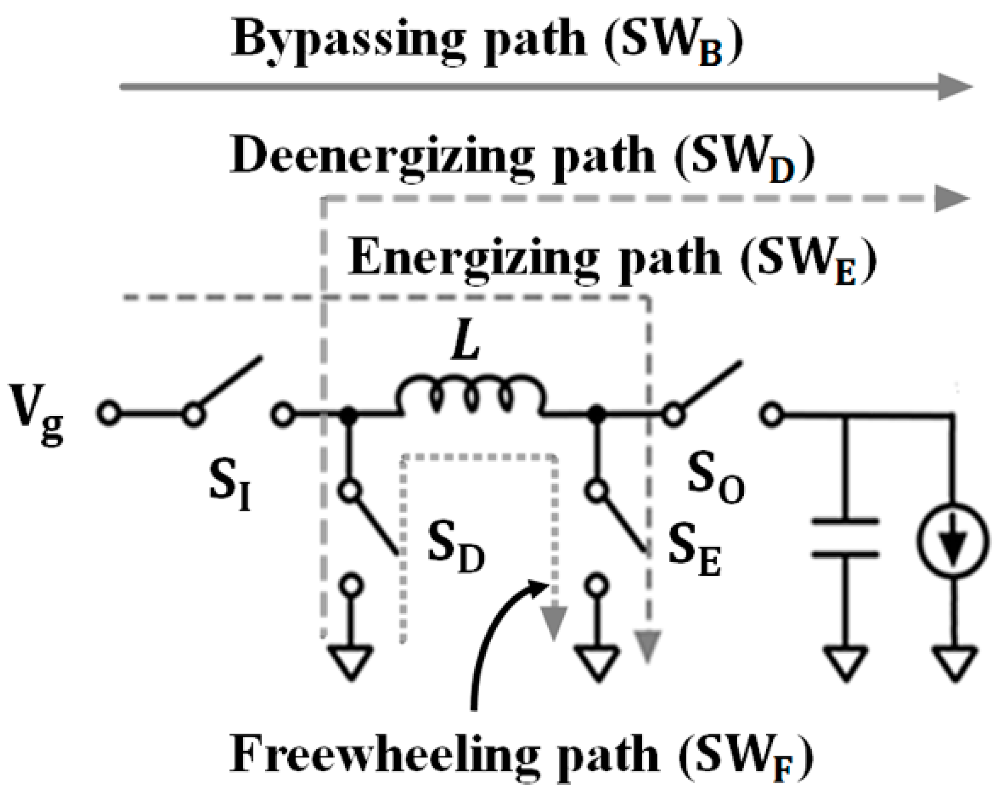
2. Proposed SIMO Architecture and Control Scheme

In this section, we introduced the operational principle, condition setting of the deep boost, and architecture of the proposed SIMO auto-buck-boost DC–DC converter with EDRC.

2.1. Error-driven Randomized Control (EDRC) for Auto Buck-Boost SIMO Converter

We used the power stage shown in Figure 2, which is from a non-inverting buck-boost DC–DC converter in the proposed converter, which is capable of simultaneously regulating buck and boost outputs.
Figure 3a, b illustrates inductor current waveforms of two operation modes, inductor power switching mode A ( IPSM A   ) and inductor power switching mode B ( IPSM B ), respectively. IPSM A mode charges energy in inductor with the energizing phase (TE) and delivers the energy to one of the outputs with the de-energizing phase (TD), while IPSM B delivers energy to an output with the bypassing phase (TB). If outputs within the range of a typical buck ( V O   <   V g   or   V O     V g ) or mild boost type ( V O   >   V g ) are operated in IPSM A and outputs within the range of the deep boost type ( V O     V g ) are operated in IPSM B , then the converter can support auto-buck-boost as in the control scheme in [19], assuming that regulation is achieved.
We denote the duty of IPSM A as D A , and the duty of IPSM B as D B . If we set D A to always be wider than D B , then the transition of the operation mode from IPSM A to IPSM B for any output can increase the charge supplied to that output, without affecting the size of the time intervals for the next outputs. The relation of D A and D B can be expressed as follows:
D A =   D B   +   β
Here, β is the difference in duty between the two modes and positive. Next, the relationships of the charges supplied to any output of IPSM A and IPSM B can be approximated as follows:
Q B     Q A   +   T S     β     I i
Here, I i is the inductor current level at the start of an energizing phase. The derivation of Equation (2) is explained in Appendix A. Thus, the transition of the mode from IPSM A to IPSM B for any output can increase the charge supplied to that output by T S β I i , and the increase in the duration of power delivery for the output does not reduce the size of the time intervals for the next output. In this study, we utilized the operation modes IPSM A and IPSM B with the adoption of β, to adjust the inductor current level and amount of charge supplied to the outputs.
The duty ratios of both modes ( D A and D B ) were controlled so that the sum of the output errors becomes zero, as in the case of the EBC scheme of [14]. We set the duty difference β of the two operation modes to a constant value for simplicity. For a mode transition from I P S M A to I P S M B to raise the inductor current, the condition of Δ I L A < Δ I L B should be satisfied. The condition is expressed as follows:
Δ I LB     Δ I LA = (   V O L     β   +   V g L     V g L     D A )   T S   >   0
Here, we set the value of β to satisfy the condition in Equation (3).
Figure 4a–c shows the waveforms of the proposed EDRC scheme under a steady state, positive step change, and negative step change, respectively, where we presumed that output 1 is of the deep boost type. At the preceding edge of each switching period, the output errors were sampled. The output having the maximum output error was selected based on a comparison of the output errors; the output error was the voltage level resulting from subtracting the output voltage from the reference voltage. We denoted the output error as V error .
In Figure 4a, we presumed that load requirement in output 2 is the lowest among all outputs; therefore, the slope of V error 2 is the lowest among all outputs while increasing. This makes output 2 the least selected. The error-based output selection also flexibly controls the frequency of selection of the outputs. In Figure 4b, the rise in the load requirement in output 2 at t 1 increased the slope of V error . It increased the frequency of the selection of output 2. In Figure 4c, the decline in the load requirement in output 2 at t 4 decreased the frequency of selection of output 2. This flexible error-based output selection helped to mitigate load regulation.
The control circuit assigns the operation mode to the selected output at the preceding edge of the switching period. In the following, we will explain the criteria for assigning the operation modes.
The proposed converter should raise the inductor current level or widen the power delivery duration in response to a rise in the load requirement. A rise in the load requirement results in an increase in the sum of the output errors. Therefore, the proposed converter monitors the sum of the output errors to detect variations in the load requirement. We denoted the sum of the output errors by V error _ sum . We adopted two reference voltage levels, V ref + and V ref , for detecting the increase or decrease in V error _ sum . The reference voltage levels, V ref + and V ref , are voltage levels of the same magnitude but different signs, as shown in Figure 4. V error _ sum was sampled at the preceding edge of the switching period, and the control circuit assigns an operation mode based on a comparison of V error _ sum with V ref + and V ref .
If the sampled V e r r o r _ s u m is sensed to be smaller than V r e f + but greater than V r e f , that is V r e f +   >   V e r r o r _ s u m   >   V r e f , then the average inductor current level should be maintained. The control circuit assigns I P S M A to an output within the range of the typical buck type ( V O   <   V g   o r   V O     V g ) or mild boost type ( V O   >   V g ). The combination of T E and T D in I P S M A allows for auto-buck-boost regulation to be achieved [24]. The control circuit assigns I P S M B to an output within the range of the deep boost type ( V O     V g ), as in [19]. We will cover the criteria for determining the range of the deep boost type in the next section. In Figure 4a, all sampled V e r r o r _ s u m values were sensed to be V r e f +   >   V e r r o r _ s u m   >   V r e f . Therefore, outputs 2 and 3 were operated in I P S M A , and output 1 was operated in I P S M B .
Provided that the sampled V_(error_sum) was greater than V_(ref+), i.e., V_(error_sum) > V_(ref+), the control circuit assigned IPSM_B, to increase both the inductor current level and power delivery duration. In Figure 4b, the rise in the load requirement in output 2 at t_1 increased the slope of V_(error_sum), raising the sampled V_(error_sum) above V_(ref+) between t_2 and t_3. Accordingly, all selected outputs were operated in IPSM_B between t_2 and t_3 as indicated by the N2 mark, whereas IPSM_B (indicated by the N1 mark) was assigned for supplying the deep boost output. The operation mode of outputs 2 and 3 was switched from IPSM_A to IPSM_B. The mode transition instantaneously increased the inductor current level. In particular, IPSM_B of buck output 3 increased the inductor current level for the entire switching period. This instantaneous adjustment in the inductor current level led to an improvement in the drivable load current and cross-regulation. However, the instantaneously increased inductor current level might cause the output ripple voltage to rise instantly. The simulation and experimental results will show how the output ripple voltage was increased.
If the sampled V error _ sum is sensed to be lower than V ref , i.e., V error _ sum   <   V ref , then the control circuit assigns IPSM A , to decrease both the inductor current level and power delivery duration. In Figure 4c, the decrease in the load requirement of output 2 at t 4 reduced the sampled V error _ sum below V ref after t 5 . Thus, all selected outputs were operated in IPSM A after t 5 until the sampled V error _ sum was increased over V ref . The mode transition from IPSM B to IPSM A of output 1 led to a reduction in the inductor current level.
When all outputs are fully supplied, the selection of any output forces that output to be supplied with more load current than it demands, wasting power and increasing the output ripple voltage. Therefore, in such cases, the converter does not select any output. We denoted this technique as "no demand no selection (NDNS). We adopted the reference voltage V r e f _ N S for determining whether all outputs are sufficiently supplied, as shown in Figure 4c. If the control circuit senses that all sampled output errors at the preceding edge of a switching period are lower than V r e f _ N S , then it freewheels the inductor current without selecting outputs, as indicated by the N3 mark.

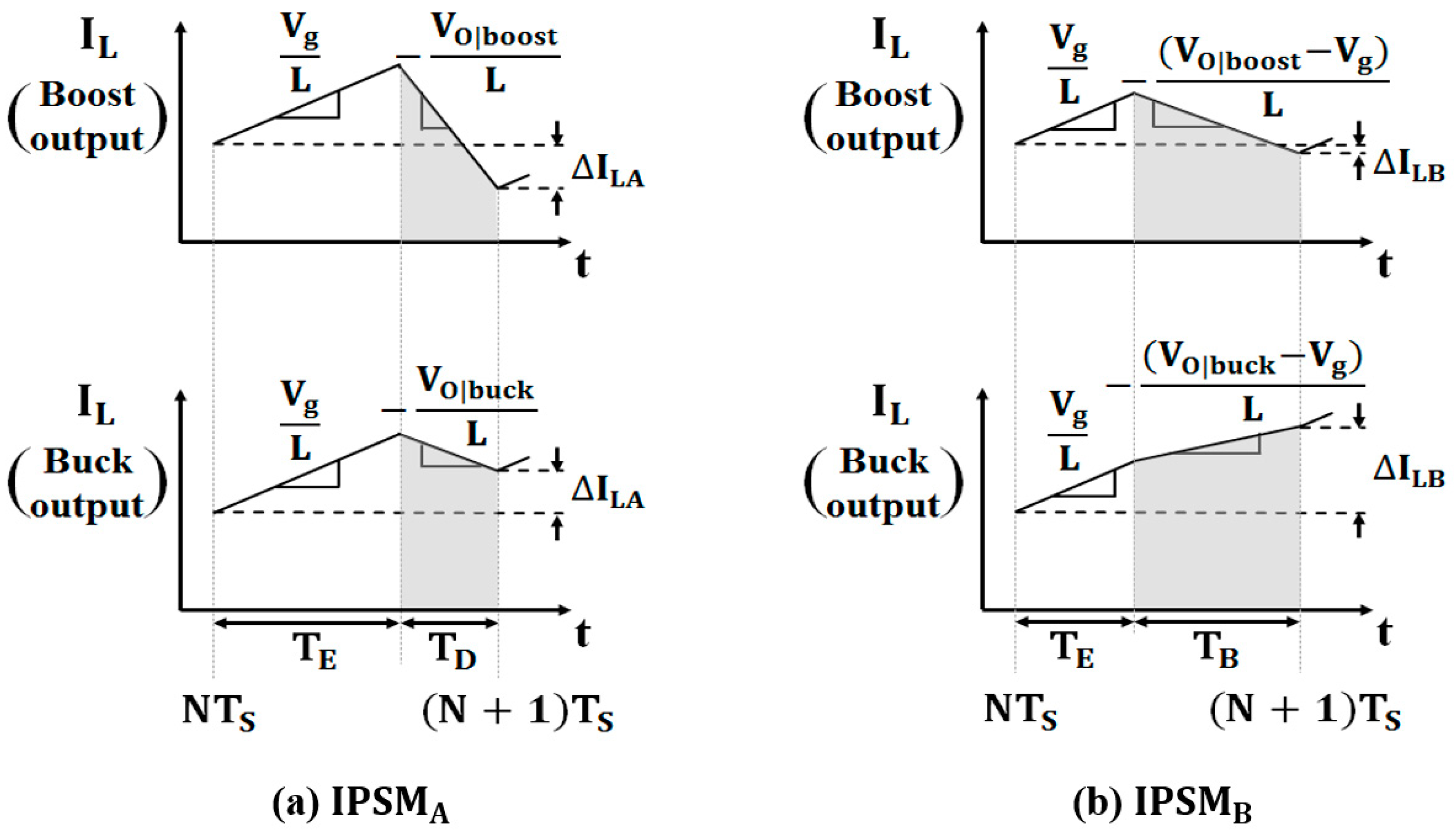
2.2. Condition Setting of Deep Boost

We set the range of the deep boost based on a comparison of the input voltage and scaled-down output voltage, as follows:
V g   <   α     V O
where α is a constant scalar factor. We will provide a guideline for choosing α in this section. If V g increases from below α V O to above α V O , then the operation mode of the output is switched from IPSM B to IPSM A , assuming that the sampled V error _ sum is sensed to be between V ref + and V ref . However, the inductor current changes of IPSM A and IPSM B for one switching period, i.e., Δ I LA and Δ I LB , are different. Consequently, a mode transition may cause a change in the inductor current level, resulting in an overshoot of the output voltages.
Figure 5 shows a simulated average overshoot voltage waveform corresponding to α in the proposed converter, in a case where increasing V g changes the operation mode of output 2. The constant scalar factor α is mathematically in the range between 0 and 1. When α is 0.5, the boundary level for determining the operation mode, V g =   α V O , is 1.5 V. In the simulation, 1.5 V of V g was too small to achieve regulation of the output voltage. Therefore, we simulated the average overshoot voltage by varying α in the range between 0.6 and 1. Within this range, an average overshoot voltage below 60 mV was guaranteed. Thus, a designer can set α to ensure that the average overshoot voltage does not exceed a specified value. We selected α as 0.7, as this value produced the lowest average overshoot voltage for the results in Figure 5.

2.3. Architecture of the Proposed EDRC

Figure 6 shows a block diagram of the proposed EDRC scheme. The analog subtractor comprises of one op-amp and four resistors, and produces the output error voltage. In the maximum output error selector (MOES) block, comparator circuits compare the output errors with each other, and the MOES block selects the output having the maximum output error. An analog adder (comprising one op-amp and four resistors) aggregates the output error voltages to produce V (error_sum). Comparator circuits compare each output error voltage with V (ref_NS) to sense when all outputs are fully supplied. The EDRC operates in a DCM mode when the inductor current becomes zero during the power delivery duration. The zero current detection block detects when the inductor current becomes zero, and is implemented by adopting the method in [1,25]. The IPSM block determines the operation mode of the output selected by the MOES block. The truth table for the IPSM block is summarized in Table 1.
The combination of T E and T D allows for the control-to-output transfer function of IPSM A to have right half plane (RHP) zero [26,27,28,29]. The RHP zero causes a phase lag, and results in the phase margin being negative [26,27,28,29]. To make the phase margin positive, multiple works in [29,30] employed a Type III compensation network. Therefore, we employed a Type III compensation network to compensate for V error _ sum as well, as shown in the duty timing controller (DTC) block.
In the DTC block, the comparator circuit produced a pulse width modulation (PWM) signal for IPSM A , based on receiving the compensated V error _ sum and ramp signal V rampA . Likewise, another comparator circuit produced a PWM signal for IPSM B , based on receiving the compensated V error _ sum and ramp signal V rampB (which was delayed by β T S as compared to V rampA ). The mux block selected one of two PWM signals for receiving the output signal of the IPSM block.
The control logic and gate driver block stored the inputs at the rising edge of CLK; the CLK signal is a clock signal whose period is T S . The rising edge of the CLK signal and the falling edge of V rampA were synchronized.

3. Simulation Results

In this section, we used MATLAB to simulate a version of the proposed converter with three outputs, to verify its effectiveness. The simulation environment includes V g = 2 V, V o u t 1 = 3.3 V, V o u t 2 = 2.5 V, V o u t 3 = 1.5 V, f S = 781 kHz, L = 5.8 μ   H, C o u t 1 = C o u t 2 = C o u t 3 = 10 μ   F, α = 0.7, and β = 0.19.
Figure 7 shows simulated waveforms of the output voltages of the proposed EDRC scheme, in a case where the sampled V e r r o r _ s u m was sensed to be within V r e f +   >   V e r r o r _ s u m   >   V r e f . The outputs were randomly selected. Output 3 was operated in I P S M B and outputs 1 and 2 were operated in I P S M A , according to a comparison of V g with α V O . The pulse width in S O 3 was wider than those of the remaining outputs; this determined the operation modes of the outputs. The load current of output 3 was 330 mA, i.e., the largest among all outputs. Therefore, output 3 seems to be the most frequently selected. However, the wider power delivery duration of I P S M B allowed for more power to be received in one switching period than in the cases of outputs 1 and 2. Therefore, output 3 was the least selected output from among all outputs, even though output 3 had the largest load current among all outputs.
Figure 8a, b shows the simulated transient waveforms of the proposed EDRC scheme, where we measured the maximum driving current, load regulation, and cross-regulation. We compared the measurements with the performances measured in the SIMO auto-buck-boost DC–DC converter of [19], based on the PCCM scheme. Figure 8c shows the simulated transient waveforms of the proposed EDRC scheme, but without the NDNS technique. We show the effectiveness of the NDNS technique through a comparison of Figure 8b,c.
In Figure 8a, 0.372 mV/mA and 0.012 mV/mA were the simulated values of load regulation and cross-regulation in response to a driving current of 250 mA, respectively. In Figure 8b, 0.18 mV/mA and 0.01 mV/mA were the simulated values of load regulation and cross-regulation, respectively. The work in [19] achieves 2 mV/mA and 0.67 mV/mA of load regulation and cross-regulation in response to a maximum driving current of 110 mA, respectively. In reality, the load requirement varies, in units of mA/ms. To show the change in the inductor current level and increase in the output ripple voltage, Figure 8 shows the results of simulating extreme cases, in which an increase or decrease in a load current of 250 mA occurred in 1 ns. Nevertheless, the performances of the load regulation, cross-regulation, and maximum driving current as simulated in Figure 8 are improved over those in [19].
The proposed EDRC scheme instantaneously adjusted the inductor current level in response to a change in the load requirement. In Figure 8a, it allowed the inductor current to rise from 0.97 A to 1.3 A with only five cycles, in response to an increase in load current of 250 mA. The instantaneous adjustment of the inductor current level by the proposed EDRC scheme led to improvements in the performances of the load regulation, cross-regulation, and output driving capability.
In Figure 8c, the load and cross-regulations were measured at 0.46 mV/mA and 0.164 mV/mA, respectively. The proposed EDRC scheme without the NDNS technique achieved worse performances in regards to load regulation and cross-regulation than those in Figure 8b, although it achieves better performances than those of [19]. The selection of an output that does not require a load current increased the output ripple voltage (as shown by the boxes with the dashed lines), thereby aggravating load regulation and cross-regulation.
The instantaneous adjustment in the inductor current level can abruptly increase the output ripple voltage. We assumed a worst-case scenario where the output ripple voltage increases in the proposed EDRC scheme, and show the guaranteed maximum increase in the output ripple voltage from the simulation. The worst-case scenario is that the average inductor current level is elevated, and the operation mode is switched from I P S M A to I P S M B . We modeled the increase in the output ripple voltage of the scenario in Appendix A, as expressed in Equation (A5). We plotted Equation (A5) regarding D A in Figure 9. Figure 9 shows that the increase in output ripple voltage was guaranteed to be less than 65 mV.
Figure 10 shows the waveforms of the output voltages and inductor current where V g was increased from 1.7 to 3.4 V and decreased from 1.7 to 3.4 V at a slope of 0.4 V/ms. The sections of the graph in Figure 10a that are marked by “(b)”, “(c)”, “(d)”, and “(e)” (4 μ   s in width) were enlarged in Figure 10b–e, respectively. In these sections, the sampled V e r r o r _ s u m was sensed to be within V r e f +   >   V e r r o r _ s u m   >   V r e f . In Figure 10b, the outputs 3, 2, and 1 operated in I P S M B , I P S M B , and I P S M A , respectively, depending on the relationship between V g and V O i α . Likewise, in Figure 10c, the outputs 3, 2, and 1 operated in I P S M B , I P S M A , and I P S M A , respectively, and in Figure 10d,e all outputs operated in I P S M A . The proposed EDRC scheme maintained constant output voltages by switching the operation mode seamlessly, according to the variation of V g .

4. Experimental Results

We implemented the power stage of the proposed converter and analog part of the control circuit with discrete components, and the digital part of the control circuit with field-programmable gate arrays. Figure 11 shows the photography of the implemented converter on the PCB board. The specifications and component values for the proposed converter are summarized in Table 2. Figure 12 shows the measured waveforms of the output voltages and gate-drive signal on switch S E in a case where the sampled V error _ sum was sensed to be between V ref + and V ref . The output voltage of each output rose, in random order. Outputs 3, 2, and 1 operated in IPSM B , IPSM A , and IPSM A , respectively, depending on the relationship between V g and V Oi α   . The operation mode of each output can be confirmed by the pulse width of the gate-drive signal applied to switch S E . In the waveform of the gate-drive signal, two types of pulse widths are shown, “wider width” and “narrower width”. The “wider width” pulse represents IPSM A , and the “narrower width” pulse represents IPSM B . This waveform also shows that one of the output voltages increased randomly while the duty was low in the steady state.
Figure 13 shows the measured transient waveforms. In Figure 13a,b, the load current of output 3 was changed from 33 to 220 mA and from 220 to 33 mA, respectively, where the load currents in the cases of outputs 2 and 1 were I out 2 = 250 mA, and I out 1 = 220 mA, respectively. Figure 13c,d shows the load current change in output 2 from 7 to 284 mA and from 284 to 7 mA, respectively, where I out 1 = 220 mA, and I out 3 = 150 mA. Figure 13e, f shows the load current change in output 1 from 5 to 205 mA and from 205 to 5 mA, respectively, where I out 1 = 220 mA, and I out 2 = 250 mA. The load and cross-regulations were measured as 0.27 mV/mA and 0.042 mV/mA, respectively, which were based on the calculation of measurement in Figure 13c.
In Figure 13c, the output ripple voltages of outputs 1, 2, and 3 increased from 55 to 76 mV, from 42 to 102 mV, and from 53 to 70 mV, respectively, after the occurrence of the transient load. At 0.1 W of total output power, 85.5% efficiency was achieved. At 1.28 W of the total output power, the maximum efficiency of 91.2% was achieved, as shown in Figure 14. To confirm the improvement in efficiency when employing the NDNS technique, we also measured the efficiency when not employing the NDNS technique, as shown by the dashed line in Figure 14. The adoption of the NDNS technique achieved an improvement in efficiency of 1.3% at 0.1 W.

5. Discussions

The operation of the proposed converter was verified in the simulation and experimental results sections. In this section, we discussed the performance improvements and techniques that lead to the advantages over the techniques in previous articles. Table 3 compares the performances between the previous and proposed works. In the simulation results, we described the structural advantage of the proposed instantaneous adjustment of the inductor current level in regards to the output driving capability, load regulation, and cross-regulation. The proposed converter achieved 0.042 mV/mA of cross-regulation and 0.27 mV/mA of load regulation in response to a change in load current of 277 mA. Table 3 shows the performance improvements compared to those of the previous works, except for the load regulation of the EBC control in [14].
The EBC control selects outputs based on output errors to improve efficiency in light loads, and employs an add-on linear regulator to alleviate cross-regulation. We introduced a technique for mitigating cross-regulation by adjusting the inductor current level without a linear regulator, and extend the output selection technique based on output errors to an auto-buck-boost topology.
We introduced the NDNS technique. As shown in Figure 8c in the three dashed-line boxes, the power of 0.45 W was over-supplied. The NDNS technique can save the wasted power. Figure 14 shows that the NDNS technique resulted in an increase of efficiency. An efficiency of 85.5% in the case of the proposed converter was achieved at 0.1 W of the total output power, an improvement over the previous works.
In addition, in our simulation results, we have shown how the NDNS technique could improve performances in the cross-regulation, load regulation, and output ripple voltage. However, an instantaneous adjustment in the inductor current level may cause an abrupt increase in the output ripple voltage. We modeled the increase in the output ripple voltage of the proposed converter in the simulation section. The simulation results show that the increase in output ripple voltage was guaranteed to be less than 65 mV. An increase in the switching frequency can reduce the increase in the output ripple voltage.
To reduce the average inductor current level, the work in [20] allows for the operation modes of outputs within the range of typical buck or mild boost types to include a bypassing cycle. In our scheme, it would be possible to lower the average inductor current level if IPSM A were to include a bypassing cycle. However, we allowed IPSM A to consist of only energizing and de-energizing cycles, to reduce the circuit complexity and to instantaneously adjust the inductor current level.
We employed filtering capacitors with a capacitance larger than that of the quoted previous publications in Table 3, as the discrete components used in this study limited the speed of the converter. However, we expected that on-chip fabrication of the proposed converter would increase the switching frequency, and thereby enable the use of 10   μ F capacitors. The operation of the proposed converter with 10 μ F filtering capacitors was verified through simulation.

6. Conclusions

In this study, we proposed a SIMO auto-buck-boost DC–DC converter with error-driving randomized control. We extended an output selection technique based on output errors to an auto-buck-boost topology, and introduced a technique for instantaneously adjusting the inductor current level. In addition, we introduced the NDNS technique, which does not select any output when the loads are sufficiently supplied. The proposed EDRC scheme achieves performance improvements in efficiency in regards to light loads, cross-regulation, and output driving capability in SIMO auto-buck-boost DC–DC converters.

Author Contributions

H.P. implemented the methodology as well as validating the proposed method and results. S.K. supervised the overall research. All authors have read and agreed to the published version of the manuscript.

Funding

This research was supported by the MSIT (Ministry of Science and ICT), Korea, under the “ICT Consilience Creative Program” (IITP-2019-2017-0-01015) supervised by the IITP (Institute for Information & Communications Technology Planning & Evaluation).

Acknowledgments

The authors performed this work as a part of research projects under the Yonsei Global Talent Fostering Program supported by SK Hynix.

Conflicts of Interest

The authors declare no conflict of interest.

Appendix A

In the Appendix A, we derived Equation (A2) and the equation for the increase in the output ripple voltage of the worst-case scenario in the proposed EDRC, which was employed to plot the waveforms in Figure 9. The amounts of charge supplied to the output of operation mode IPSM A and the output of operation mode IPSM B are driven by Equations (A1) and (A2), respectively, where I i denotes the initial value of the inductor current.
Q A   =   D A T S ( I i + V g L D A T S V O 2 L D A T S )
Q B   =   Q A + T S β I i + T S 2 { V g L D A β V O 2 L D A β + ( D A + β ) 2 L ( V g D A V O β V g β ) }
In Equation (A2), the T S 2 term is negligible as compared with the remaining terms. Therefore, Equation (A2) is approximated by Equation (A2).
Figure A1 illustrates a worst-case scenario of an increase in the output ripple voltage. In this scenario, the operation mode is changed from IPSM A to IPSM B , and the average inductor current level is increased from I L | avr ( m ) to I L | avr ( n ) , where I L | avr is the average inductor current level, m is the time before the output ripple voltage increase, and n is the time after the output ripple voltage increase. The increases in the output ripple voltages during the power delivery durations of t m and t n are expressed by Equations (A3) and (A4), respectively.
Δ V O | D A = D A T S ( I L | avr ( m ) I O ( m ) ) / C out
Δ V O | D B   =   D B T S ( I L | avr ( n ) I O ( n ) ) / C out
The increase in the output ripple voltage is derived by subtracting Equation (A3) from Equation (A4), and is expressed as follows:
Δ V O | D A Δ V O | D B   =   [ D A { ( I L | avr ( n ) I L | avr ( m ) ) ( I O ( n ) I O ( m ) ) }   + β ( I L | avr ( n ) I O ( n ) ) ] T S / C out
Figure A1. Illustration of the worst-case scenario of the increase in an output ripple voltage in the proposed EDRC scheme, where the average inductor current level is increased, and the operation mode is changed from IPSM A to IPSM B .
Electronics 09 01335 g0a1

References

  1. Ma, D.; Ki, W.H.; Tsui, C.Y.; Mok, P.K. Single-inductor multiple-output switching converters with time-multiplexing control in discontinuous conduction mode. IEEE J. Solid-State Circuits 2003, 38, 89–100. [Google Scholar]
  2. Ma, D.; Ki, W.H.; Tsui, C.Y. A pseudo-CCM/DCM SIMO switching converter with freewheel switching. IEEE J. Solid-State Circuits 2003, 38, 1007–1014. [Google Scholar]
  3. Koon, S.-C.; Lam, Y.-H.; Ki, W.-H. Integrated charge–control single-inductor dual-output step-up/step-down converter. In Proceedings of the IEEE International Symposium on Circuits and Systems, Kobe, Japan, 23–26 May 2005; pp. 3071–3074. [Google Scholar]
  4. Jia, J.; Leung, K.N. Digital-control single-inductor triple-output dc-dc converter with pre-sub-period inductor-current control. IEEE Trans. Power Electron. 2012, 27, 2028–2042. [Google Scholar] [CrossRef]
  5. Patra, P.; Patra, A.; Misra, N. A single-inductor multiple-output switcher with simultaneous buck, boost, and inverted outputs. IEEE Trans. Power Electron. 2012, 27, 1936–1951. [Google Scholar] [CrossRef]
  6. Le, H.-P.; Chae, C.-S.; Lee, K.-C.; Wang, S.-W.; Cho, G.-H.; Cho, G.-H. A single-inductor switching dc-dc converter with five outputs and ordered power-distributive control. IEEE J. Solid-State Circuits 2007, 42, 2706–2714. [Google Scholar] [CrossRef]
  7. Woo, Y.; Le, H.-P.; Cho, G.-H.; Cho, G.-H. Load-independent control of switching DC-DC converters with freewheeling current feedback. IEEE J. Solid-State Circuits 2008, 43, 2798–2808. [Google Scholar] [CrossRef]
  8. Chae, C.-S.; Le, H.-P.; Lee, K.-C.; Cho, G.-H.; Cho, G.-H. A single-inductor step-up DC-DC switching converter with bipolar outputs for active matrix OLED mobile display panels. IEEE J. Solid-State Circuits 2009, 44, 509–524. [Google Scholar] [CrossRef] [Green Version]
  9. Lee, Y.-H.; Huang, T.-C.; Yang, Y.-Y.; Chou, W.-S.; Chen, K.-H.; Huang, C.-C.; Lin, Y.-H. Minimized transient and steady-state cross regulation in 55-nm CMOS single-inductor dual-output (SIDO) step-down dc-dc converter. IEEE J. Solid-State Circuits 2011, 46, 2488–2499. [Google Scholar] [CrossRef]
  10. Zhang, Y.; Ma, D. Adaptive pseudo-continuous conduction mode operation schemes and circuit designs for single inductor multiple output switching converters. J. Analog Integr. Circ. Signal Process. 2012, 72, 419–432. [Google Scholar] [CrossRef]
  11. Shen, Z.; Chang, X.; Wang, W.; Tan, X.; Yan, N.; Min, H. Predictive digital current control of single-inductor multiple-output converters in CCM with low cross regulation. IEEE Trans. Power Electron. 2012, 27, 1917–1925. [Google Scholar] [CrossRef]
  12. Patra, P.; Ghosh, J.; Patra, A. Control scheme for reduced cross regulation in single-inductor multiple-output dc-dc converters. IEEE Trans. Ind. Electron. 2013, 60, 5095–5104. [Google Scholar] [CrossRef]
  13. Lu, D.; Qian, Y.; Hong, Z. An 87%-peak-efficiency DVS-capable single-inductor 4-output DC-DC buck converter with ripple-based adaptive off-time control. In Proceedings of the 2014 IEEE International Solid-State Circuits Conference Digest of Technical Papers (ISSCC), San Francisco, CA, USA, 9–13 February 2014; pp. 82–84. [Google Scholar]
  14. Jung, M.Y.; Park, S.H.; Bang, J.S.; Cho, G.H. An error-based controlled single-inductor 10-output dc-dc buck converter with high efficiency under light load using adaptive pulse modulation. IEEE J. Solid-State Circuits 2015, 50, 2825–2838. [Google Scholar] [CrossRef]
  15. Xu, W.; Li, Y.; Hong, Z.; Killat, D. A 90% peak efficiency single-inductor dual-output buck-boost converter with extended-PWM control. In Proceedings of the 2011 IEEE International Solid-State Circuits Conference, San Francisco, CA, USA, 20–24 February 2011; pp. 394–396. [Google Scholar]
  16. Zhou, S.; Zhou, G.; Liu, G.; Mao, G. Small-signal Modeling and Cross-regulation Suppressing for Current-mode Controlled Single-inductor Dual-output DC-DC Converters. IEEE Trans. Ind. Electron. 2020. [Google Scholar] [CrossRef]
  17. Wang, Y.; Xu, J.; Yin, G. Cross-Regulation Suppression and Stability Analysis of Capacitor Current Ripple Controlled SIDO CCM Buck Converter. IEEE Trans. Ind. Electron. 2019, 66, 1770–1780. [Google Scholar] [CrossRef]
  18. Zheng, Y.; Ho, M.; Guo, J.; Leung, K.N. A single-inductor multiple-output auto-buck-boost dc-dc converter with tail-current control. IEEE Trans. Power Electron. 2015, 31, 7857–7875. [Google Scholar] [CrossRef]
  19. Zheng, Y.; Ho, M.; Guo, J.; Mak, K.-L.; Leung, K.N. A single-inductor multiple output auto-buck-boost dc-dc converter with autophase allocation. IEEE Trans. Power Electron 2015, 31, 2296–2313. [Google Scholar] [CrossRef]
  20. Zheng, Y.; Guo, J.; Leung, K.N. A Single-Inductor Multiple-Output Buck/Boost DC–DC Converter with Duty-Cycle and Control-Current Predictor. IEEE Trans. Power Electron. 2020, 35, 12022–12039. [Google Scholar] [CrossRef]
  21. Wei, C.L.; Chen, C.H.; Wu, K.C.; Ko, I.T. Design of an average-current mode noninverting buck-boost DC-DC converter with reduced switching and conduction losses. IEEE Trans. Power Electron. 2012, 27, 4934–4943. [Google Scholar] [CrossRef]
  22. Yao, C.; Ruan, X.; Cao, W.; Chen, P. A two-mode control scheme with input voltage feed-forward for the two-switch buck-boost DC-DC converter. IEEE Trans. Power Electron. 2014, 29, 2037–2048. [Google Scholar] [CrossRef]
  23. Lee, Y.-J.; Khaligh, A.; Emadi, A. A compensation technique for smooth transitions in a noninverting buck-boost converter. IEEE Trans. Power Electron. 2009, 24, 1002–1016. [Google Scholar]
  24. Erickson, R.W.; Maksimovic, D. AC equivalent circuit modeling. In Fundamentals of Power Electronics, 2nd ed.; Kluwer Academics: Secaucus, NJ, USA, 2001; pp. 187–263. [Google Scholar]
  25. Jing, X.; Mok, P.K.T.; Lee, M.C. A wide-load-range constant-charge-auto-hopping control single-inductor-dual-output boost regulator with minimized cross-regulation. IEEE J. Solid-State Circuits 2011, 46, 2350–2362. [Google Scholar] [CrossRef]
  26. Ki, W.-H. Signal flow graph in loop gain analysis of DC-DC PWM CCM switching converters. IEEE Trans. Circuits Syst. I Fundam. Theory Appl. 1998, 45, 644–655. [Google Scholar]
  27. Wu, W.-C.; Bass, R.M. Eliminating the effects of the right-half plane zero in fixed frequency boost converters. In Proceedings of the PESC 98 Record. 29th Annual IEEE Power Electronics Specialists Conference, Fukuoka, Japan, 22 May 1998; pp. 362–366. [Google Scholar]
  28. Lee, J.J. Analysis of a Small-Signal Model of a PWM DC-DC Buck-Boost Converter in CCM. Master’s Thesis, Wright State University, Dayton, OH, USA, 2007. [Google Scholar]
  29. Linear Technology, LTC3536 Datasheet. Available online: https://www.analog.com/en/products/ltc3536.html (accessed on 18 August 2020).
  30. Sahu, B.; Rincon-Mora, G.A. A low voltage, dynamic, noninverting synchronous buck-boost converter for portable applications. IEEE Trans. Power Electron 2004, 19, 443–452. [Google Scholar] [CrossRef]
Figure 1. Illustrated example waveforms of output voltage of a single inductor multiple output single inductor multiple output (SIMO) converter with three outputs. Control scheme utilizing (a) sequential-order-based output selection [6,7,19,20], and (b) error-based output selection of [14].
Electronics 09 01335 g001
Figure 2. Power stage of a single inductor buck-boost DC–DC converter and switching control modes of inductor current paths.
Electronics 09 01335 g002
Figure 3. Illustrating inductor current waveforms of two inductor power switching mode modes (a) energizing and then de-energizing phases (we named the inductor power switching mode A (IPSMA)) and (b) energizing and then bypassing phases (named IPSMB). The proposed error-driven randomized control (EDRC) employs both inductor power switching modes.
Electronics 09 01335 g003
Figure 4. Illustrated transient waveforms of the proposed EDRC scheme under (a) steady state, (b) a positive step change and (c) a negative step change of load current in output 2. We presume that output 1 is of the deep boost type ( V O V g ). The IPSM B indicated by N1 mark is assigned for supplying the deep boost output, the IPSM B indicated by N2 is assigned for increasing the inductor current level, and the Φ NS indicated by N3 mark is the inductor current freewheeling phase where no output is selected.
Electronics 09 01335 g004
Figure 5. Simulated average overshoot voltage waveform in terms of α of the proposed EDRC scheme, in the case where increasing V g changes the operation mode of output 2. The simulation environment is as follows: V g = 2 V, V O 1 = 1.5 V, V O 2 = 2.5 V, and V O 3 = 3.3 V.
Electronics 09 01335 g005
Figure 6. Block diagram of the proposed EDRC. Black lines with an arrow represent an analog signal, and gray lines with an arrow represent a digital signal.
Electronics 09 01335 g006
Figure 7. Simulated waveforms of output voltages, gate-drive voltages for output switches, and inductor current while sampled V error _ sum is sensed to be within V ref +   >   V error _ sum   >   V ref .
Electronics 09 01335 g007
Figure 8. Simulated transient waveforms of the proposed EDRC (a) under a positive step change of load current in output 2 from 10 to 260 mA and (b) under a negative step change of load current in output 2 from 260 to 10 mA. (c) Simulated transient waveforms of the EDRC without adopting the no demand no selection (NDNS) technique under a negative step change of load current in output 2 from 260 to 10 mA. The dashed boxes show when power supply exceeded demand.
Electronics 09 01335 g008
Figure 9. Simulated waveforms of the increase in output ripple voltage in terms of D A when the average inductor current level rises. The simulation is performed based on Equation (A5). The load current is (a) 100 mA, (b) 330 mA, and (c) increased from 50 to 330 mA.
Electronics 09 01335 g009
Figure 10. (a) Simulated transient waveforms of out voltage of each node and inductor current while Vg increases from 1.4 to 3.4 V and decreases from 3.4 to 1.4 V. In order to display details of transient signals, Figure from (b) to (e) show enlarged parts marked by (b)–(e) in Figure 10 (a).
Electronics 09 01335 g010
Figure 11. Fabricated SIMO auto-buck-boost DC–DC converter. It is implemented with discrete components on PCB board. In the PCB, there are 5 outputs, but only 3 outputs were used in the experiments.
Electronics 09 01335 g011
Figure 12. Measured waveforms of output voltages and gate-drive signal on switch SE while the sampled is sensed to be between and where = 2 V, = 100 mA, = 104 mA, and = 53 mA.
Electronics 09 01335 g012
Figure 13. Measured transient waveforms of outputs, when one of output load–current changes abruptly, for all cases supply voltage V g is 2 V. For each figure, the out load current changed as indicated. Load current of output 3 was changed from 33 to 220 mA (a), from 220 to 33 mA (b). The load current of output 2 changes from 7 to 284 mA (c), and from 284 to 7 mA (d). For Figure (e) and Figure (f), load current of output 1 changes from 5 to 205 mA (e), and from 205 to 5 mA (f), respectively.
Electronics 09 01335 g013
Figure 14. Solid line is the measured efficiency of the proposed EDRC scheme versus total output power. Dashed line is measured efficiency without adopting the NDNS technique.
Electronics 09 01335 g014
Table 1. Truth table of output of inductor power switching mode (IPSM) block.
Conditions Based on Comparison of Magnitude of InputsOutput
V r e f + > V e r r o r _ s u m > V r e f V g >   α V O ( i ) 0 ( IPSM A )
V g <   α V O ( i ) 1 ( IPSM B )
V error _ sum >   V ref + -1 ( IPSM B )
V error _ sum <   V ref -0 ( IPSM A )
Table 2. Specifications and component values of the proposed converter.
Number of Channels3
Vg1~3.5 V (2 V nominal)
Vout1, Vout2, and Vout31.5 V, 2.5 V, 3.3 V
Switching frequency195 kHz
L(DCR)5.8 μ H (5 m Ω )
Cout1, Cout2, and Cout3(ESR)39 μ F (15 m Ω )
α 0.7
β 19%
Table 3. Comparison of performance with previous publications.
Ref [14] Ref [18] Ref [19] Ref [20] Present Work
Published Year2015201620162020-
Implementation Discrete component0.35   μ m CMOS0.35   μ m CMOS0.35   μ m CMOSDiscrete component
Input voltage (V)4.851.85–2.92.51.7– 3.4
Number of outputs210443
Output voltages (V)3.3, 1.23.3 (3), 2.8 (2), 2.5 (2), 1.8 (3)3.3, 3, 2.5, 1.83.4, 3, 2.5, 1.83.3, 2.5, 1.5
Switching frequency (MHz)0.10.70.250.75~10.195
Peak efficiency (%)7888.78989.591.2
Light-load efficiency77%@0.11 W83.5%@0.14 W7%@0.2 W83%@0.15W85.5%@0.1 W
Auto-buck-boostNoNoYesYESYes
Output driving capability (mA)100185110300277
Load-regulation (mV/mA)10.1720.560.27
Cross-regulation (mV/mA)0.50.10.670.050.042

