Review

Supply-Scalable High-Speed I/O Interfaces

1
Department of Electrical Engineering and Computer Sciences, University of California at Berkeley, Berkeley, CA 94720, USA
2
Ayar Labs, Santa Clara, CA 95054, USA
Electronics 2020, 9(8), 1315; https://doi.org/10.3390/electronics9081315
Submission received: 25 July 2020 / Revised: 12 August 2020 / Accepted: 13 August 2020 / Published: 15 August 2020
(This article belongs to the Special Issue Low-Voltage Integrated Circuits Design and Application)

Abstract

:
Improving the energy efficiency of computer communication is becoming more and more important as the world is creating a massive amount of data, while the interface has been a bottleneck due to the finite bandwidth of electrical wires. Introducing supply voltage scalability is expected to significantly improve the energy efficiency of communication input/output (I/O) interfaces as well as make the I/Os efficiently adapt to actual utilization. However, there are many challenges to be addressed to facilitate the realization of a true sense of supply-scalable I/O. This paper reviews the motivations, background theories, design considerations, and challenges of scalable I/Os from the viewpoint of computer architecture down to the transistor level. Thereafter, a survey of the state-of-the-arts fabricated designs is discussed.

1. Introduction

Nowadays, there are huge demands on a smarter world for better human convenience and happiness (i.e., manufacturing, smart city, autonomous vehicle, security…). In order to realize those, it is inevitable that we have to create, replicate, and process tremendous amount of data [1]. For example, ref. [2] forecasts that the amount of data will increase by more than 3× in five years. Handling those explosive data is a large burden on computer communications in the current computer architecture [3]. As a result, high-speed input/output (I/O) standards used for computer communications are evolving very rapidly, and moreover, new I/O standards are also being introduced to address various needs. In accordance with those trends, multi-standard I/O transceivers (transmitter and receiver) are getting a huge attention from industry to provide considerable flexibilities to IC products [4,5,6,7,8,9,10,11]. To support multiple standards with a single transceiver design, it needs to be flexible for a variety of specifications, especially for a wide range of operating data rates. In addition, even for the cases of dealing with a single I/O standard, many standards require backward compatibility to their own legacy generations; for example, PCI Express, USB, serial ATA, etc.; thus, the wide-range operation is also very important [12,13].
However, implementing such wide-range capability introduces a large burden on the I/O design. Before deep diving into what the burden is, we briefly review the overall I/O transceiver architecture and how it works. As shown in the overall block diagram in Figure 1, the I/O transceiver is composed of three big parts: clock generation, a transmitter (TX), and a receiver (RX) [14]. In the clock generation, a phase-locked loop (PLL) is generally used to generate a high-frequency clock for the high-speed I/O from a low-frequency reference clock. These days, a half-rate clock (e.g., 14 GHz for 28 Gb/s NRZ datastream, also referred to as a double-data rate (DDR) clock) and a quarter-rate clock (i.e., 7 GHz for 28 Gb/s NRZ, also referred to as a quarter-data rate (QDR) clock) are generally used. The clock generation circuitry can be shared across multiple transmitter and receiver lines to amortize the area and power consumption [15,16,17]. The high-frequency clock is distributed to the individual transmitters and receivers with a clock buffer chain. Depending on the macro floorplan, the distribution distance can be a few hundred µm or even longer; a long chain of buffers needs to be used so that the distribution circuit consumes a significant amount of power. In addition, the high-speed clock may experience duty-cycle distortion and phase skew across the chain because of inherent device mismatch and duty-cycle error amplification [18,19]. As a result, a duty-cycle correction (DCC) circuit or a quadrature error correction (QEC) circuit is frequently used at the transmit side to correct such distortions for better eye opening at the transmitter output. Based on the timing information from the corrected clock, parallel input data are serialized into a high-speed bitstream (serializer). The serialized data stream is transmitted through the transmission line driven by the TX output driver, whose output impedance is supposed to match with the characteristic impedance of the transmission line for signal integrity. To compensate inter-symbol interference (ISI) due to the channel loss at high frequency, a feed-forward equalizer (FFE), which combines multiple adjacent bits to cancel out the ISI effect, is frequently implemented at the transmit side. To adapt with various channel conditions and receiver sensitivity, the output voltage swing is configurable. On the receiver side, the received data is usually highly distorted by the ISI due to the limited channel bandwidth. Therefore, a continuous time linear equalizer that boosts high-frequency gain is generally placed at the front-end of the receiver. RX slicers are used to decide whether the received analog signal is ‘1’ or ‘0’ by sampling the signal at the timing when the signal-to-noise ratio (SNR) is maximized. A variable-gain amplifier (VGA) can be preceded by the slices to amplify the input signal for better sensitivity. Since it is important to sample the received signal when the SNR is maximized, finding the optimum sampling timing is one of the utmost tasks of the receiver. The clock and data recovery (CDR) circuit collects such timing information from edge slicers (bang-bang CDR) or error slicers (baud-rate CDR), and based on the collected information, it adjusts the sampling timing by using a phase interpolator (PI) [20]. A multi-phase generation circuit such as a delay-locked loop (DLL) or an injection-locked oscillator (ILO) is widely used to provide a high enough number of phases for the PI. On the other hand, a decision-feedback equalizer (DFE) is used to fully compensate the residual ISI. The basic concept of the DFE is to utilize the previously received data stream to help the decision of the currently received bit to compensate the ISI. Unlike the FFE or continuous-time linear equalizer (CTLE), the DFE does not degrade the SNR, so nowadays, it has become a very essential building block of the receiver. Finally, the recovered data is de-serialized to the parallel stream.
As mentioned before, introducing wide-range operation results in significant overhead on design complexity and an energy/area efficiency penalty as well. For example, because it is not easy to cover the entire frequency range with a single PLL or a single voltage-controlled oscillator (VCO), multiple PLLs (or VCOs) are frequently implemented together and are selected with respect to the operating frequency. In addition, most of the building blocks needs to be designed to work properly at the highest rate. It leads to a significant impact on the energy efficiency at a lower data rate. For better understanding, Figure 2 shows a simple example of a CMOS inverter. The delay (τd) and rise/fall time (approximately 2τd) of a CMOS inverter is proportional to the fan-out of the inverter, which is a ratio of the gate output capacitance over the gate input capacitance. To retain a full rail-to-rail CMOS swing and to reduce jitter generation, the rise/fall time must be fast enough for given operating frequency. As a rule of thumb, τd should be no larger than one-fourth of bit period (Tbit) [21,22]. It implies that the fan-out has to be low enough to sustain a proper operation at the highest frequency. On the other hand, the dynamic switching power consumption of a CMOS inverter chain whose final output load is CL is given as
P = F O F O 1 C L V D D 2 f c l k
where FO, VDD, and fclk represent the fan-out of the chain, the supply voltage, and the switching frequency, respectively [23]. That means that if the fan-out is set for the optimum operation at the highest frequency, then in fact, it is overkill and causes unnecessary power consumption at a lower frequency. In addition, there are also overheads to make circuits work at a low frequency, which makes the efficiency at high frequency worse (i.e., capacitors). These observations can be proven from the survey of wide-range and supply-scalable transceivers shown in Figure 3, where the energy efficiencies of transmitters, receivers, and transceivers in [15,16,22,24,25,26,27,28,29,30,31,32,33,34,35] are marked in the scatter plot with respect to how wide the operating range is (highest data rate/lowest data rate). Note that the energy efficiencies depicted in the Figure 3 are measured at the highest data rate of each design. It is observed that the energy efficiency becomes worse as the range widens, which proves the overhead of the wide range.
To resolve such efficiency loss due to the wide-range operation, introducing supply scalability, whose impact has been already well-demonstrated in microprocessors and Internet of Things (IoT) applications [36], to the I/O transceiver has been proposed. The basic concept is to lower the supply voltage when the I/O works at low speed where it does not require full voltage due to the relaxed bandwidth, in order to reduce the power consumption, which is similar to the concept of dynamic voltage and frequency scaling (DVFS) of microprocessors [24,37,38,39,40]. More details on the supply-scalable I/O interfaces will be discussed in the following section.

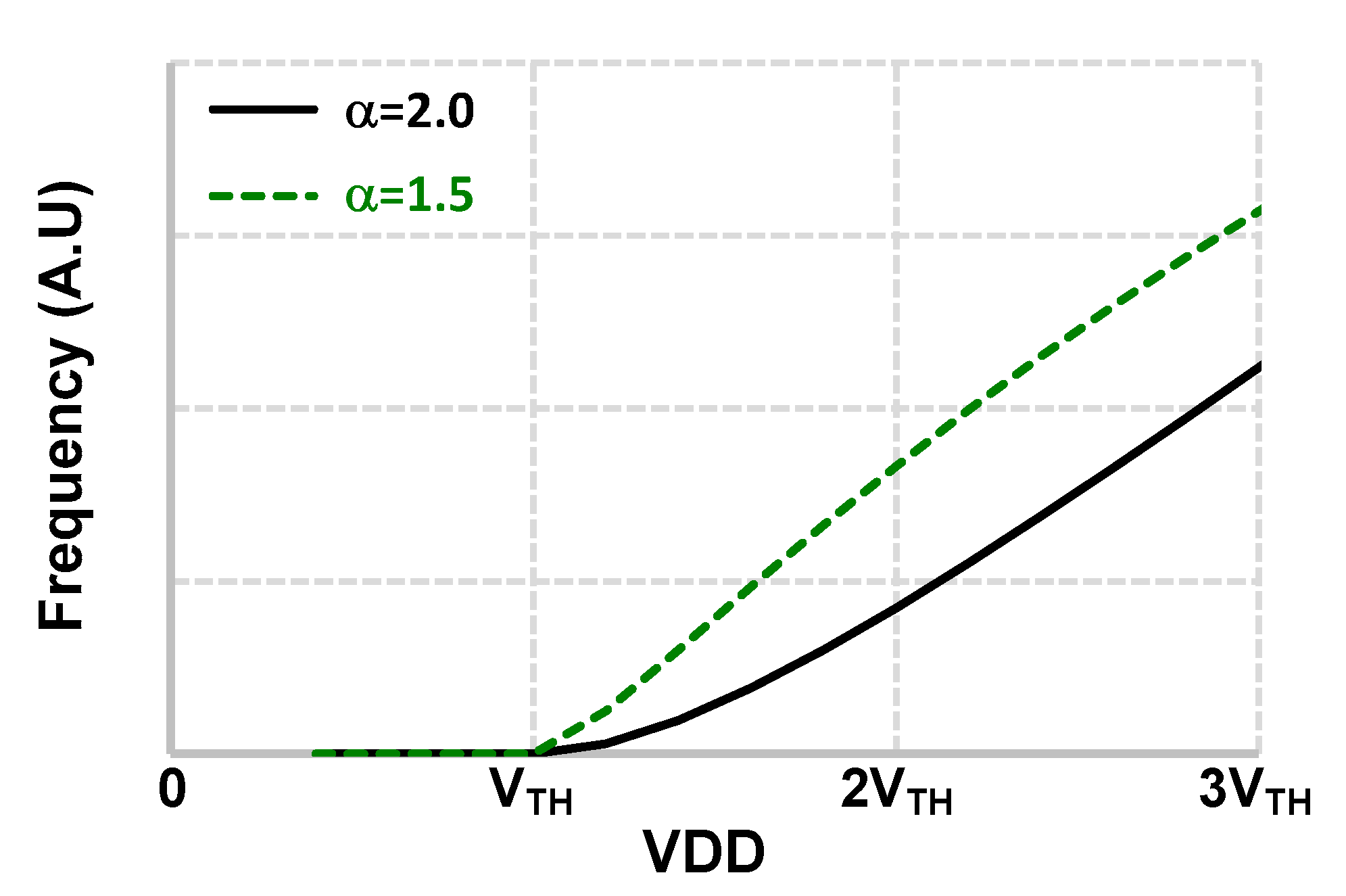
2. Basic Concept of Supply-Scalable I/O

In addition to the demands on the multi-standard or the backward-compatible I/Os discussed in the previous section, the fact that the link utilization of computer communications is rarely maximum is another important motivation of supply-scalable I/O [37,38,39,40]. For example, in [39], Google disclosed that the servers’ utilization is mostly between 10% and 50% of their maximum utilization levels, where they exhibit poor efficiency. For example, ref. [40] shows that if a system (servers and network) is 15% utilized while the servers are fully energy-proportional, the network will then consume nearly 50% of the overall power, which is a huge waste. As a result, if the communication network is able to adapt the power consumption by scaling the supply voltage according to the communication bandwidth required by the utilization, a significant energy saving is expected. In addition, recent FinFET technology offers a better performance at a lower supply voltage compared to conventional planar MOSFET, which amplifies the benefits of the supply scaling [41]. However, conventional I/O designs typically assume fixed-voltage operation. Even for some wide-range designs, the power consumption is usually dominated by the supply voltage post-fabrication; frequency scaling alone rarely saves much power but instead hurts performance [42].
To see more deeply how the supply scaling improves the energy efficiency, we review the power consumption of I/O interface circuits, which can be divided into three groups [43,44]. The first one is CMOS dynamic switching power, which is proportional to CV2f. In the block diagram of Figure 1, the serializer, deserializer, digital circuits, slicers, and some of the clocking circuits fall into this category. The second thing is the power consumption from the static current, which includes analog circuits relying on current biases—for example, amplifiers and current-mode logic (CML) buffers. The last one is the signaling power, which includes equalization circuits and TX drivers as well as the power dissipated at 50-Ω terminations. Those three types of power consumption exhibit very different aspects when the operating speed changes, which is illustrated on the left side of Figure 4. As we can easily expect from CV2f, the dynamic switching power scales linearly as the data rate scales. On the other hand, the others do not scale with the data rate. In fact, at high frequency, the signaling power increases non-linearly as the data rate increases, because extensive equalization and higher transmit swing are required to overcome the channel loss at such high frequency [25,45]. As a result, as shown in the leftmost plot of Figure 4, the total power consumption of the I/O transceiver increases linearly as the data rate increases but becomes non-linear at the high-frequency region. It also consumes considerable static power even at very low speed. The corresponding efficiency curve is illustrated in the inset plot, where we find that the efficiency is severely degraded at a low speed region. For example, ref. [40] shows that a link configured for 2.5 Gb/s consumes as much as 42% of the power for 40 Gb/s, which is ideally expected to be only 6.25%.
If we reduce the supply voltage at a lower speed, then how much we can reduce it? Basically, the supply voltage can be reduced until the circuits marginally work at the given speed. The free-running frequency of CMOS ring oscillators, which is usually used to evaluate the speed of CMOS devices, is a great indicator to see the relation between the speed and the voltage. The free-running frequency of a CMOS ring oscillator is expressed as
f = 1 2 N · β ( V D D V T H ) α C V D D ,
where N, β, VTH, and C represent the number of stages, transistor coefficient, threshold voltage of CMOS devices, and nodal capacitance of the ring, respectively [19]. α is another coefficient that characterizes a transistor performance, which equals two in the conventional long-channel devices but becomes closer to one for recent short-channel devices. (2) is illustrated in Figure 5 for α = 2 and 1.5. For both cases, we can see a linear-like relation as long as VDD is higher than VTH, so we can assume that the supply voltage can be linearly scaled with the data rate [24]. The resulting power consumption and efficiency when we apply the linear scaling of supply voltage are depicted in the right-side plot and inset in Figure 4. The power consumption by the static current scales linearly with the frequency (P = VI), while the CMOS dynamic power scales cubically (P = CV2f) [44]. On the other hand, it is assumed that the signaling power cannot scale with the supply voltage due to the SNR constraint. The resulting efficiency curve is much flatter than that without supply scaling, implying that the power consumption is almost linearly proportional to the data rate, which is the ideal case assumed in [40]. It also shows that the optimum efficiency may locate at an intermediate speed because of the signaling power, which is practically observed in many state-of-the-art engineering samples [15,27,32]. In addition, the signaling power overhead at a higher data rate can be confirmed from the survey in Figure 6, where the energy efficiencies at the highest rate of various scalable I/O designs are scattered with respect to the highest data rate. The efficiency becomes worse at a higher data rate above a certain data rate (approximately 8 Gb/s), implying the energy overhead to drive such high-speed signaling, which is originated from heavy equalization circuits and a larger signal swing [44].

3. Design Considerations of Supply-Scalable I/O

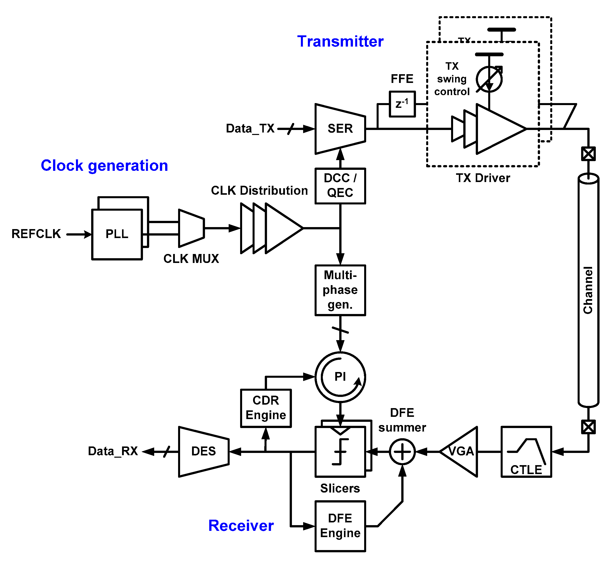
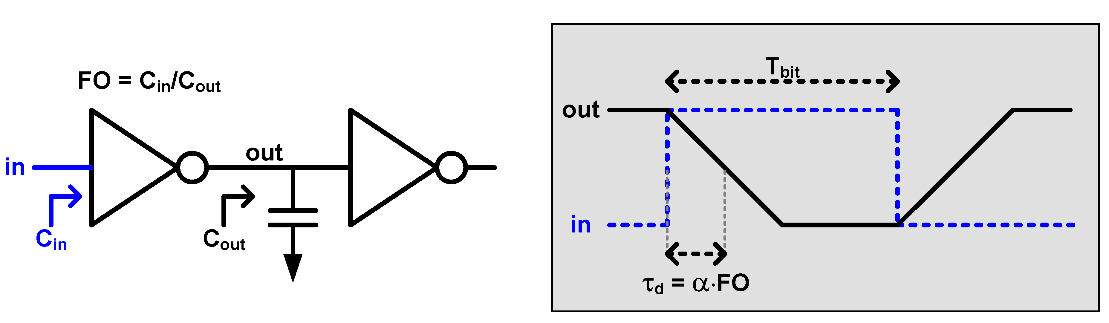
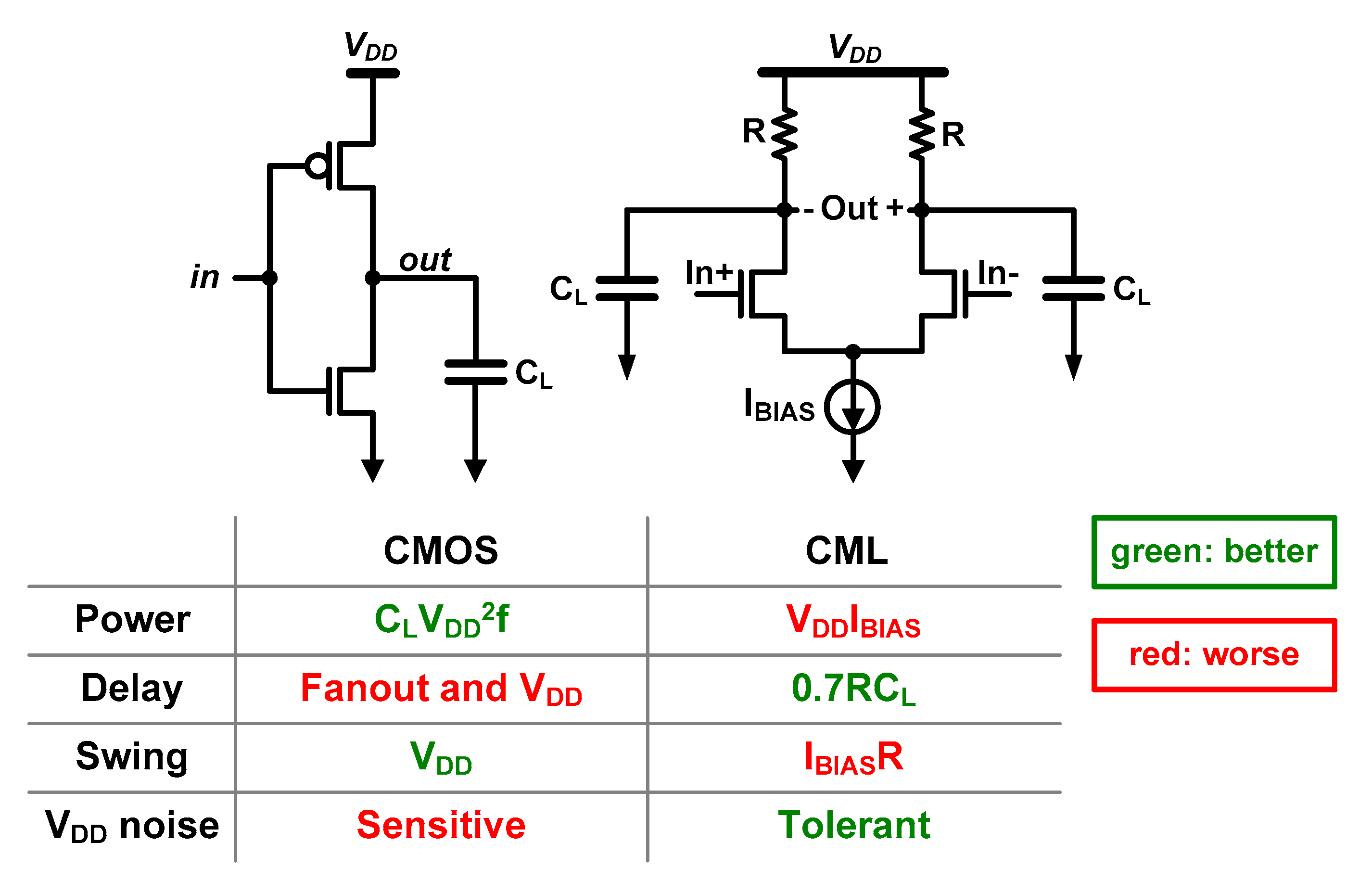
3.1. Base Circuit Topology

Figure 7 shows two major circuit topologies in CMOS technology, CMOS and CML circuits, which are most frequently used in modern analog and mixed-signal IC designs. Although current-mode logic (CML) circuits have been a majority for base circuit topology for high-speed I/O interfaces owing to their high-speed capability [46], using CMOS circuits as much as possible is preferred for supply-scalable I/O in order to maximize the frequency range and the benefit of the supply scaling [44,47]. It is mainly because the power consumption of CML circuits follows the blue line in Figure 4 (static current consumption), whereas the CMOS exhibits cubic power scaling. In addition, besides the power scaling, the CMOS circuit dissipates less power as long as the fan-out is no less than 2 [23], and it also provides a higher swing than the CML. On the other hand, the CML circuit has a much better controllability of its speed compared to the CMOS counterpart whose speed is highly deterministic to the given process technology and supply voltage. The time constant of a CML circuit is a product of the load resistance (R) and the load capacitance (CL), so tweaking R is a powerful knob of controlling the circuit speed in the design phase. The CMOS circuit can be accelerated by reducing the fan-out; however, a too-small fanout (i.e., less than 2) is not feasible in a practical circuit implementation and also results in a non-linear increase of power consumption (see (1)). As a result, the CML circuit exhibits a better capability of high-speed operation, which is a dominant issue to achieve the maximum speed of the scalable I/O. It has been one of the main reasons to make high-speed interfaces highly rely on CML circuits, although their scalability is not as good as CMOS circuits. In order to resolve this issue, ref. [25] proposed adjusting the current bias of CML circuits in accordance with the supply scaling. For example, at the minimum data rate and supply voltage (0.65 V) condition, the current bias is reduced to half of the nominal value, whereas it is raised to 1.5× when the data rate and supply voltage (1.05 V) are maximized. Instead of using a fixed resistance as CML load resistance, a symmetric load whose resistance automatically adapts with the bias current is employed in [25] to scale the circuit bandwidth while maintaining the voltage swing. As an alternative approach, a CMOS inverter with resistive feedback can be used to hit high bandwidth for fully utilizing CMOS circuits even above the CMOS limit, because the resistive feedback extends the bandwidth of the CMOS circuit at the cost of increased power consumption [48].

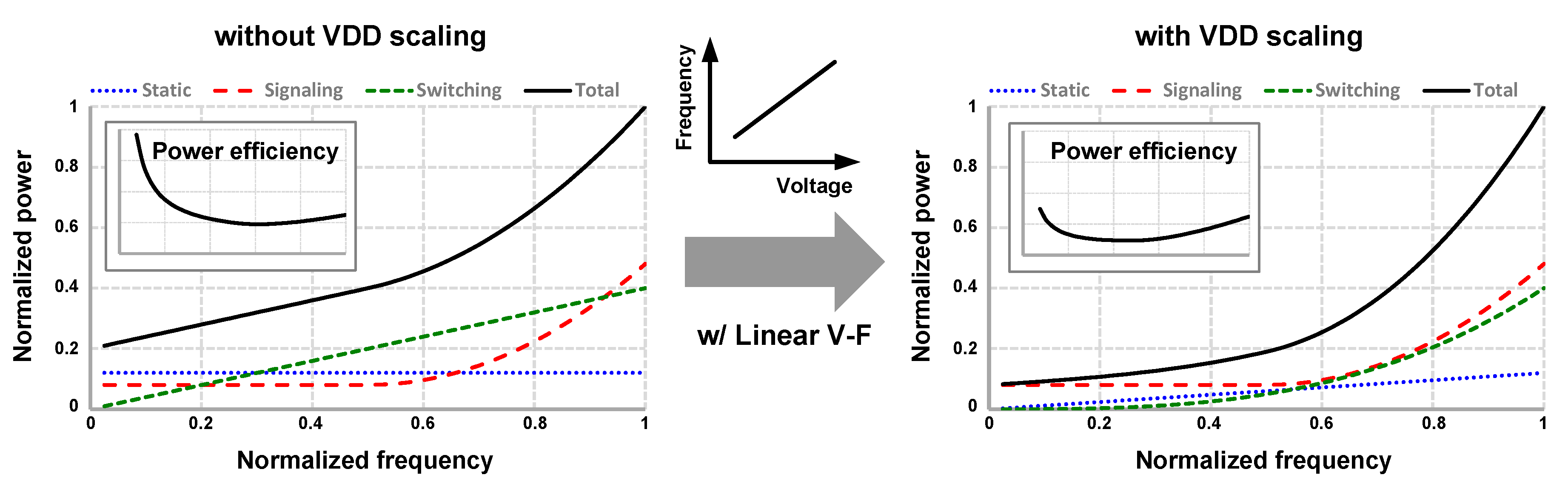
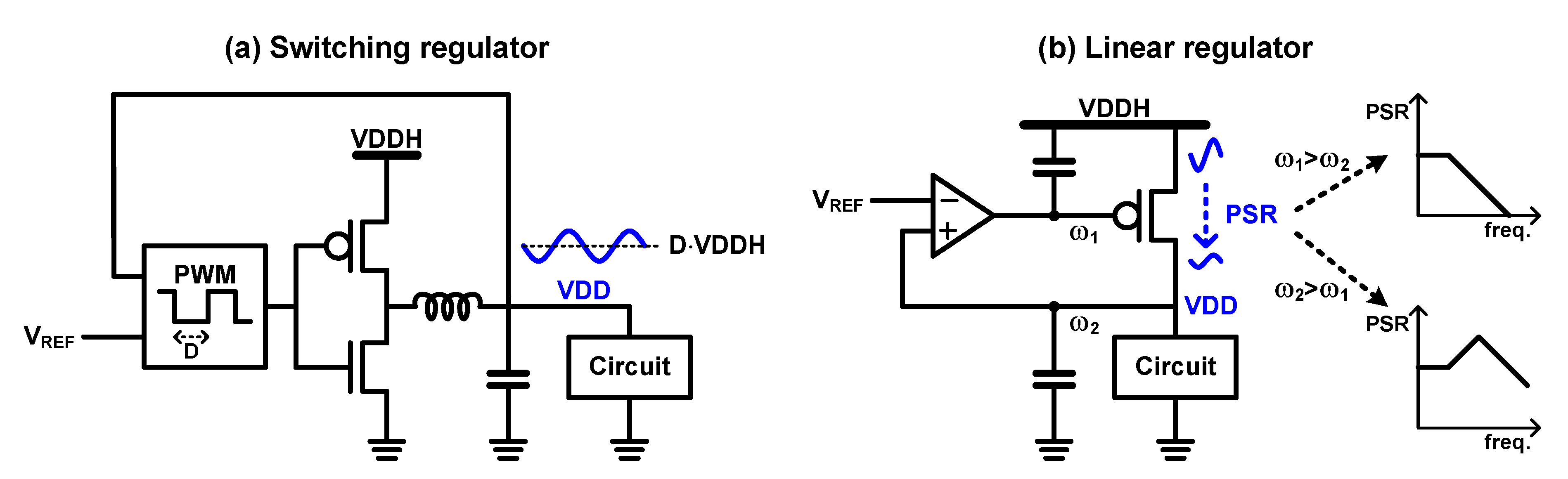
3.2. On-Chip Supply Control

From the surveys shown in Figure 3 and Figure 6, we observe there have been many works relying on off-chip supply control rather than on-chip control, and generally those works exhibit a better efficiency than those with on-chip control. It is mainly because they do not include any power overhead of supply control (either of on-chip and off-chip), so it is important to understand what the overhead is. In addition, ultimately, the supply control circuit must be integrated with the core circuits. The supply control scheme can be divided into two types: a switching regulator (DC–DC converter) and linear regulator (specifically, a low-dropout (LDO) regulator), which are depicted in Figure 8. Generally, the switching regulators exhibit higher efficiency compared to linear regulators, because there is a non-negligible voltage dropout in the linear regulators [24]. However, because of their switching behavior, the switching regulators have a periodic switching ripple on the output voltage whereas the linear regulators offer power supply noise rejection (PSR). Since most of the building blocks of high-speed I/O are very sensitive to the supply noise [49,50], the linear regulators can be more suitable for high-performance applications [12,31]. For example, [31] reveals that the link bit-error-rate (BER) degrades when a switching regulator is used. In addition, the supply sensitivity increases at a lower supply voltage, so it is more critical in supply-scalable I/O compared to fixed-supply I/O. For example, the transition delay of a CMOS inverter is approximately expressed as to
τ d = C V D D β ( V D D V T H ) α ,
where τd is the transition delay of the CMOS inverter [19]. By differentiating (3) with VDD, we can obtain the supply sensitivity of the transition delay, which represents the jitter induced by supply noise of ∆VDD as
d τ d d V D D = τ d ( 1 V D D α V D D V T H ) ,
where α equals two in long-channel devices but becomes smaller in short-channel devices, as mentioned in the Section 2. (4) is illustrated in Figure 9 for α = 2.0 and 1.5, where we find the supply sensitivity dramatically increases as the supply voltage scales [19,51]. As a result, for the case of using a switching regulator, the switching frequency and CDR bandwidth should be carefully chosen to minimize the impact of supply ripple on the link BER [22,33]. Figure 8b shows one of the design considerations of a linear regulator regarding PSR. The linear regulator is based on a negative feedback loop with two poles, one is at the output of the amplifier (ω1, gate of pass transistor) and the other is at the output (ω2, regulated supply voltage). Depending on the pole locations, the regulator exhibits different PSR characteristics. For example, if ω1 is the dominant pole (ω2 > ω1), the PSR has a peaking, whereas the opposite case exhibits a plain low-pass filter characteristic [19,52]. However, making ω2 dominant requires a huge capacitance because of low output resistance at the VDD node due to the circuit load. It costs a huge silicon area and frequently needs an off-chip capacitor, and it also severely constraints the supply transition time. To summarize, there are lots of design trade-offs (e.g., PSR versus efficiency, PSR versus silicon area), which need to be carefully examined to find the best topology and design parameters for a given application.

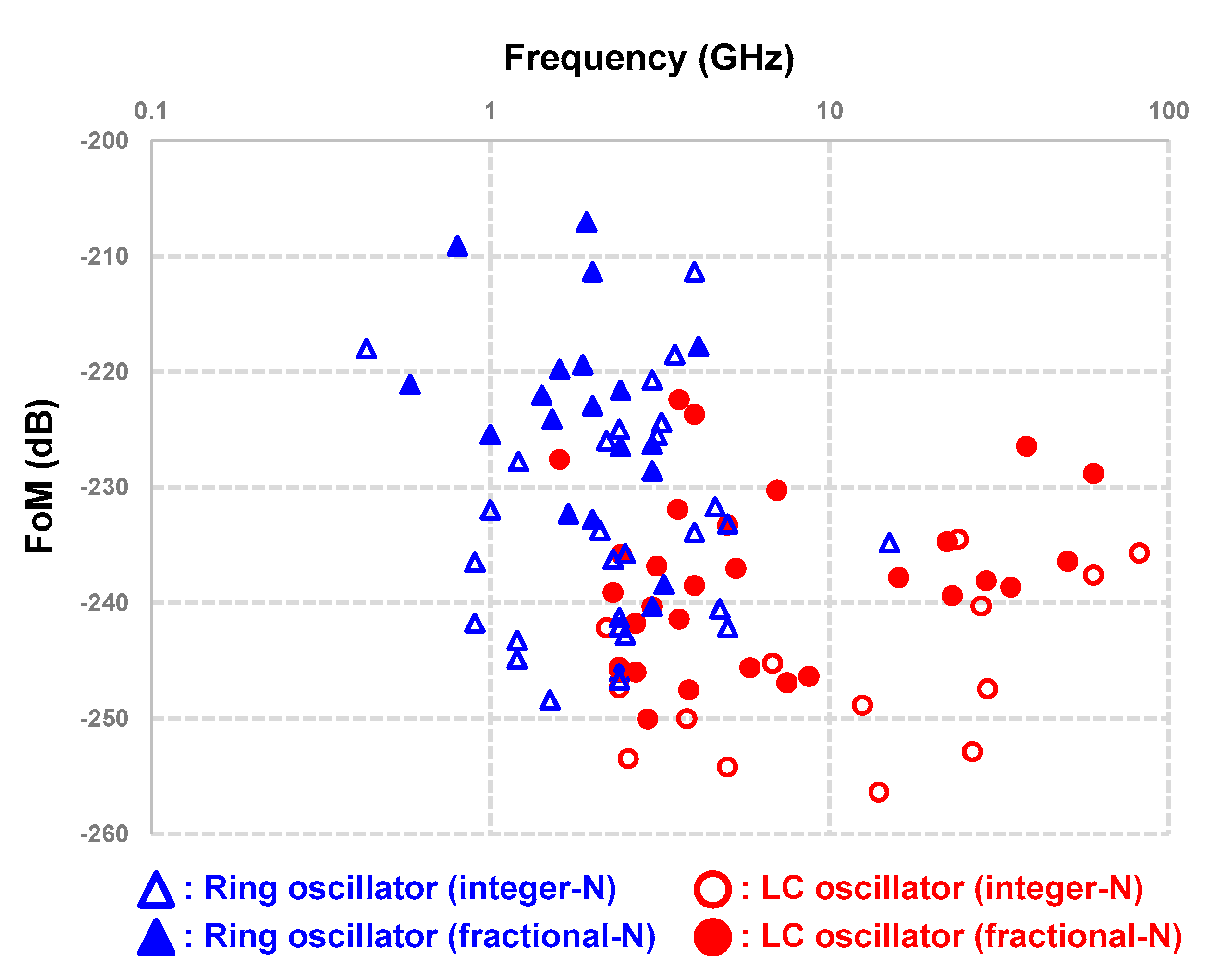
3.3. Clock Generation

As mentioned briefly in the introduction, multiple PLLs (or multiple oscillators in a single PLL) are frequently implemented in wide-range transceivers to cover the entire frequency range [4,8,10,11,53]. It is mainly because LC oscillators are popular for high-speed I/O applications because of its superior phase noise performance and high-speed capability compared to ring oscillators, and they are also less sensitive to supply voltage variation. However, LC oscillators occupy a much larger area, so using multiple LC oscillators is an expensive solution. The survey results given in Figure 10 and Figure 11 validate such trade-off between LC-based PLL and ring-based PLL. Figure 10 illustrates a scatter plot of figure-of-merit (FoM) of PLL versus operating frequency of PLL designs presented in IEEE International Solid-State Circuits Conference (ISSCC) from 2010 to 2019 [19]. The FoM of the PLL is defined as
F o M P L L = 10 log ( ( σ J 1 s ) 2 · ( P P L L 1 m W ) ) .
where σJ and PPLL denote the absolute jitter and power consumption of a PLL, respectively, which is widely used to evaluate the PLL jitter performance with equalized power consumption [54]. The trend shown in Figure 10 implies that the LC-based PLLs generally exhibit better jitter performance and higher operating frequency than the ring-based counterpart. On the other hand, we can find that the ring-based PLL occupies much less silicon area from Figure 11, where the FoM versus silicon area is plotted. In addition, the tuning range of the ring is much wider than LC [19]. As a result, the design trade-off between LC- and ring-based PLLs in wide-range I/O can be summarized as follows: the LC PLL offers better jitter performance; however, its range is limited so that no less than two LC PLLs are required to cover a wide range, which results in significant area consumption. On the other hand, the ring PLL achieves wide range with a small area; however, its higher phase noise and supply sensitivity results in worse performance. Conventionally, using multiple PLLs has been a majority option for wide-range I/O transceivers [8,10,11,55,56]. Recently, there have been some ring-based works by introducing some circuit techniques to overcome the limit of ring PLLs; for example, a two-stage ring oscillator [23], clock multiplying delay-locked loop (MDLL) [31], and multi-phase calibration [57]. For specific applications where only discrete rates are used, a single PLL with a configurable division ratio can be also used [16,58].

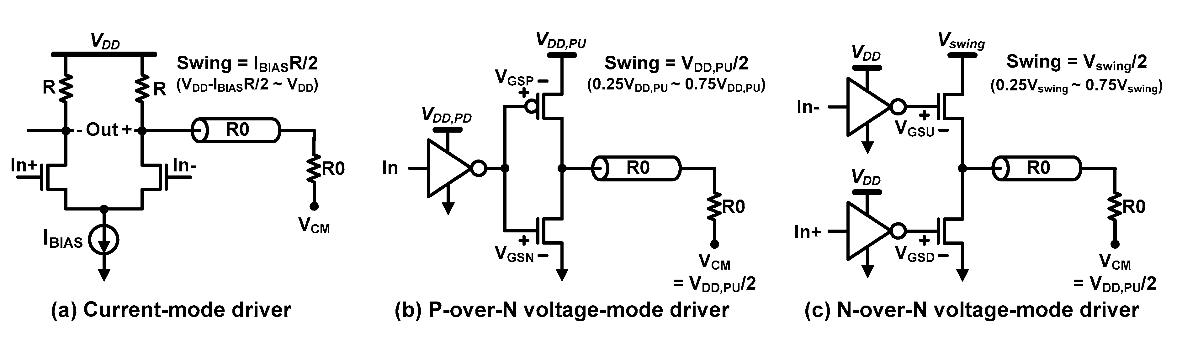
3.4. TX Driver Topology

TX output driver topology is another important factor that impacts the efficiency of scalable IO, since the TX output driver is mainly responsible for the signaling power we discussed above, although a separate supply voltage is usually dedicated for the TX driver to decouple the TX swing from the supply scaling [12,25]. The requirements for the TX driver are summarized as a proper output impedance for signal integrity, enough output swing to guarantee sufficient SNR, and optional FFE equalization for a high-loss channel. Figure 12 shows three popular topologies of TX driver implementation: a current-mode driver, P-over-N voltage-mode driver, and N-over-N voltage-mode driver [25,59,60,61,62]. In the current-mode driver, the transistors operate in the saturation region, the output impedance of the driver is generally dominated by the passive load resistance R. As a result, it provides good impedance matching across a wide range of output swing. Compared to the CML circuit that has an output swing of IBIASR, the current-mode driver has a halved swing of IBIASR/2 (single-ended), because the IBIAS splits into the load resistance and RX termination. For example, with 50-Ω termination, 20-mA current consumption is needed for 500-mV swing (=Swing/25Ω). On the other hand, the voltage-mode drivers consume less current than the current-mode driver, because there are not spilt current paths. Such a difference originates from where the termination is placed relative to the signal path, such that the termination is placed in parallel with the signal path in the current-mode driver but in series with the signal path in the voltage-mode driver. For that reason, the voltage-mode driver is also referred to the source-series terminated (SST) driver. In a P-over-N voltage-mode driver, an inverter-like PMOS-over-NMOS structure drives the channel and the RX termination. In an N-over-N voltage-mode driver, NMOS transistors are used for both pull-up and pull-down, but they are driven by an opposite polarity of input voltage. As a result, pull-up and pull-down paths are not turned on simultaneously, the current solely flows from VDD,PU (or Vswing) to VCM (or VCM to ground). As a result, assuming matched impedance for both paths, both the output swing and the common-mode voltage (VCM) are VDD,PU/2. For example, it leads to the current consumption of 5 mA for a 500-mV output swing, which is only ¼ that of the current-mode driver. The same is also applied to the N-over-N voltage-mode driver. On the other hand, the impedance matching of voltage-mode drivers is more complex than the current-mode driver, because they rely on the active devices rather than a passive resistor. Basically, the transistors should operate as a resistor to assure low output impedance so that they should be in a linear region, which constraints the gate-overdrive voltage (VOV) to be higher than the drain-source voltage (VDS). As a result, the P-over-N is more appropriate for high output swing, whereas the N-over-N fits better for low output swing [12]. A passive resistor is usually placed in series with the driver to reduce the VDS for better linearity [60,63].
As shown in Figure 12b,c, the voltage-mode drivers are driven by CMOS inverters, whereas the current-mode driver needs to be driven by a CML pre-driver, so the voltage-mode drivers are more appropriate for supply-scalable design, as we discussed in Section 3.1. However, there are constraints on the supply voltage of such inverters; hence, it limits the scalability. Since the output impedance is set by the transistors, and it is dominated by the VGS of the transistors, the supply voltage can only be adjusted in a range where the output impedance is matched within the configurable range of the driver segmentation. In the P-over-N, the VGS of PMOS and NMOS are VDD,PU and VDD,PD, respectively. In the N-over-N, the VGS of pull-up and pull-down NMOSs are VDD-VCM and VDD, respectively; therefore, the pull-up device is typically much larger to have the same impedance. For both cases, the output impedance is a function of the supply voltages of the pre-driver inverters, so the controllability on those supplies is constrained by the controllability of the output driver strength. For the supply voltage of the output driver itself, the voltage-mode driver is fully constrained by the output swing, but the current-mode driver can scale the supply until the differential pair and the current source faces a voltage headroom issue.

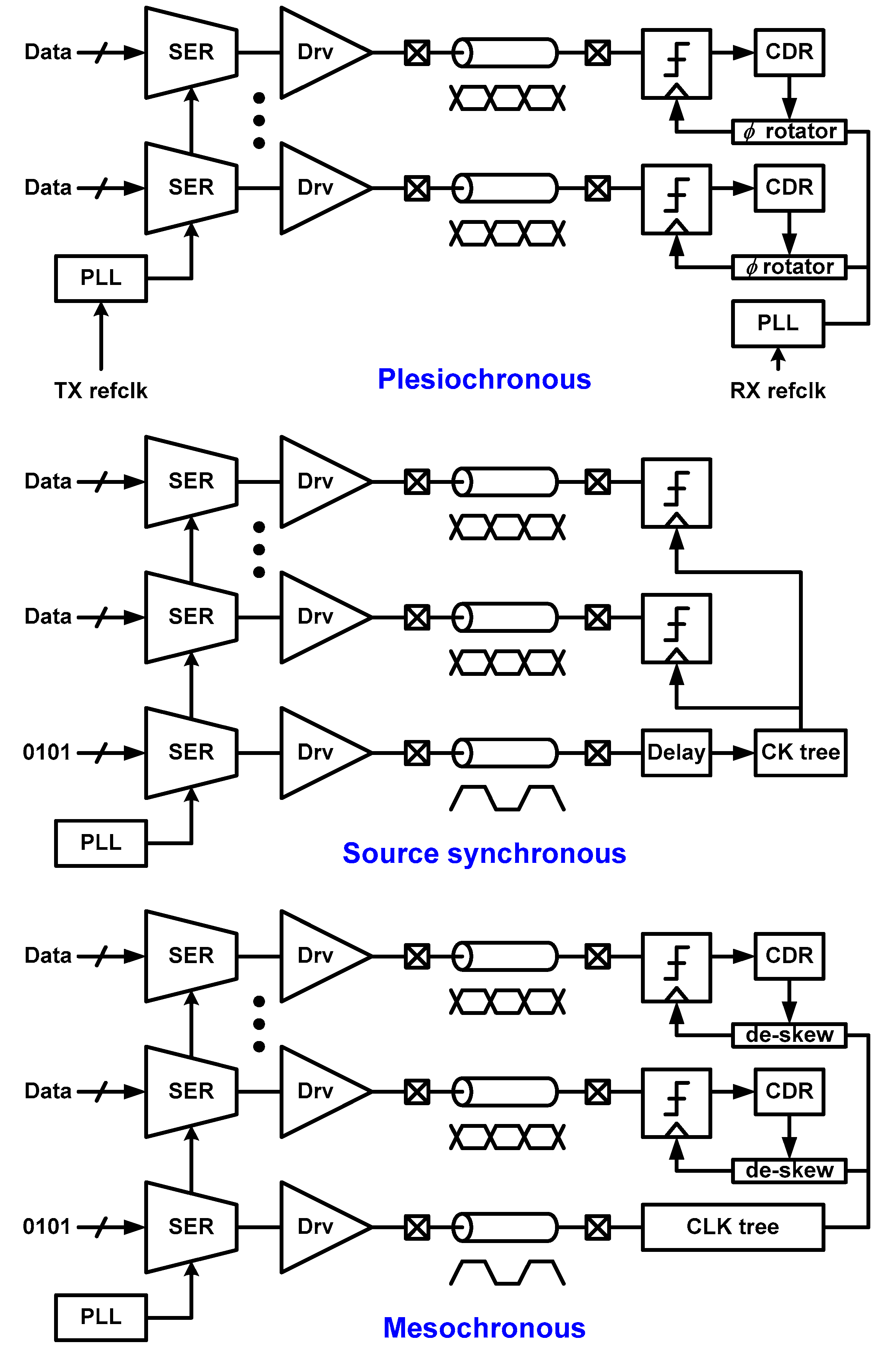
3.5. Clocking Architecture

Clocking architecture is one of the most important design choices that impacts the performance and characteristic of a generic I/O link. Sometimes, it is not choosable, as it is pre-defined in specification; nevertheless, it is still very important to understand various clocking architectures and their pros/cons. Figure 13 shows three popular clocking architectures: plesiochronous, source-synchronous, and mesochronous. In a plesiochronous link, the TX and the RX have their own PLLs, which are synchronized to different reference clock sources. As a result, there is an intrinsic frequency offset between the TX and the RX. At the receiver side, the frequency offset is tracked by rotating the sampling clock phase, which is controlled by a CDR loop. On the other hand, a source-synchronous link TX forwards its clock to the RX through a dedicated clock channel so there is no frequency offset. In addition, it is assumed that the latencies of all data channels are synchronized; hence, no per-lane phase tracking circuit is used, but the forwarded clock is simply distributed to each data lane. The delay of the data and clock paths are corrected by introducing additional delay to either TX or RX, to maximize jitter tolerance as well as eliminate static skew [64]. Compared to the plesiochronous link, the source synchronous link has a much simpler circuitry at the cost of the additional forwarded clock channel. As a result, it significantly relaxes the design complexity introduced by the supply scalability. However, it becomes impossible to eliminate the skew across data and clock lanes as the data rate increases; thus, the source-synchronous architecture cannot be a viable solution for today’s high-speed interfaces. The mesochronous link resolves such issues of the source-synchronous link with per-lane de-skew circuits. Since there is no frequency offset, the de-skew circuit does not have to rotate the phase continuously, so the circuit implementation is still simpler than the plesiochronous RX.
Parallelized architecture with a reduced clock rate but with a multi-phase clock (i.e., half-rate or quarter-rate clocking) has been one of the major innovations enabling today’s ultra-high-speed I/O with reasonable power consumption [22]. It plays a critical role in the supply-scalable I/O, because it relaxes the required circuit bandwidth at reduced supply voltages. As a result, many supply-scalable I/O designs have adopted highly parallelized architecture (e.g., quarter rate) from early works [22] to recent works [16,32,34,57]. However, the downside of parallelized architecture with scalable supply is that the mismatch effect goes worse with the scaled supply voltage [65]. As a result, duty-cycle correction (for half-rate clocking) or the multi-phase alignment technique becomes essential for supply-scalable I/O design. Specifically, for an example of quarter-rate clocking that is most popular for scalable I/O, quadrature error correction (QEC) schemes, such as phase calibration with a quadrature phase detector [47,66] or with asynchronous sampling [15,16,67] or time-division phase calibration [57,68], are widely employed.

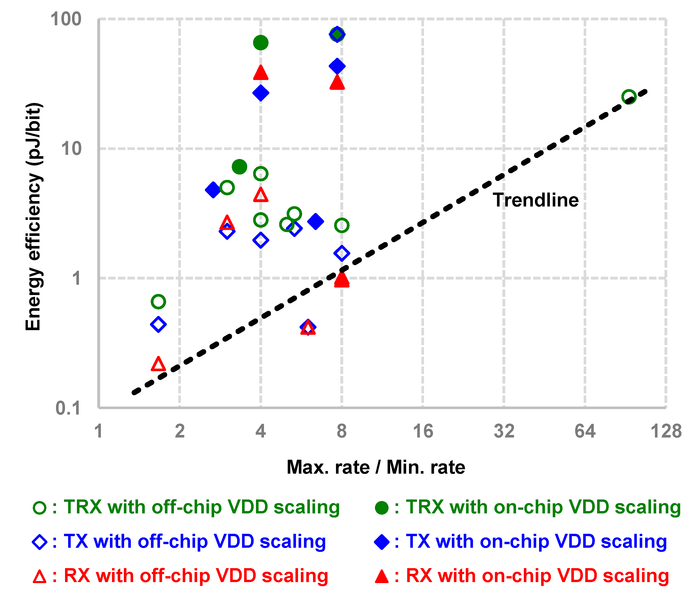
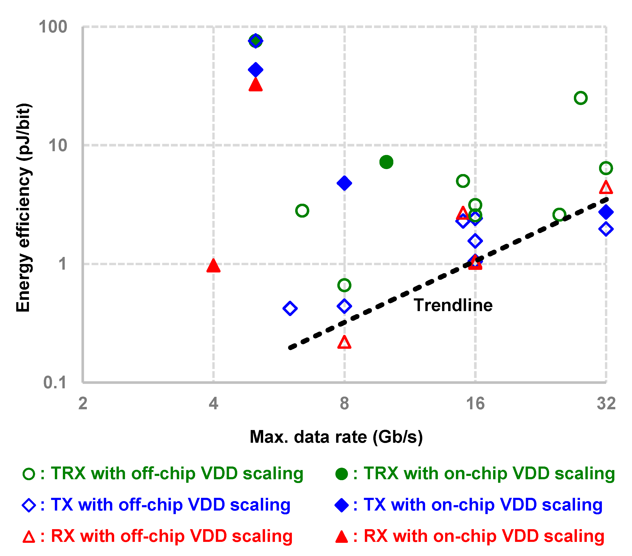
4. Survey on State-Of-The-Art Supply-Scalable I/O

In this section, we attempt to compare the previously published supply-scalable I/O designs in terms of various aspects we discussed in the previous sections. Table 1, Table 2 and Table 3 show the comprehensive review of supply-scalable transmitters, receivers, and transceivers, respectively. Note that they are sorted with oldest publication first, and the clock generation (PLL) power is included in the transmitter. Throughout the surveys, we can find various meaningful trends. First, the data rate tends to increase continuously. Second, the figure-of-merit (FoM, energy efficiency) gap between the minimum and maximum data rates has been converging as the process technology scales down. It can be interpreted as the dynamic switching power occupied the dominant portion of I/O power in older technologies (e.g., [22,24]); however, it has been significantly reduced owing to the technology scaling, whereas the others (the static current and the signaling power) have not [41,43]. Third, the quarter-rate clocking has become the major clocking architecture and tends to exhibit better energy efficiency. Lastly, as we already discussed in Figure 3 and Figure 6, the works relying on off-chip sources for supply scaling do not consider the overhead due to the supply scaling circuitry, such as non-zero energy loss, they tend to exhibit better efficiency. Only five works include the on-chip supply scaling, where the regulator efficiencies of around 80–90% have been reported.
Specifically, looking at Table 1, we can observe that the voltage-mode driver has become the mainstream topology for the transmitters for the reasons we discussed in Section 3.4. On the other hand, more than half of the transmitter works rely on the external clock source to mitigate the design complexity due to the supply sensitivity of PLL. [12,16,22,31] managed to cover the entire range with a single PLL; however, [16] uses an LC-PLL followed by a programmable divider but provides only a few quantized frequencies. [12,22,31] use a ring-PLL to cover the entire range; however, their supply voltages are separated from the other building blocks, which can also imply that it is difficult to scale the clocking circuit with the other building blocks because of its sensitivity to the supply voltage. The energy efficiency achieved from the highest data rate of each design ranges from 0.44 pJ/bit [27] to 43.3 pJ/bit [22], but we have to note that [27] does not include an equalizer, PLL, and on-chip supply scaling. If we narrow down the scope to the transmitters having at least two of them, the best energy efficiency becomes 1.97 pJ/bit at 32 Gb/s [16].
Looking into Table 2 where the survey of supply-scalable I/O receivers is presented, we can observe that mesochronous clocking has been a mainstream architecture [15,24,25,26,27], as we discuss in Section 3.5. The receiver designs that rely on external CDR/deskew calibration tend to exhibit better energy efficiency, which implies the hardware overhead of robust operation with the on-chip CDR/deskew. For example, [27] achieves 0.22 pJ/bit at 8 Gb/s from the 0.75-V supply, but [16] exhibits 1.06 pJ/bit at 8 Gb/s from the 0.72-V supply. Note that it does not mean the overhead is almost 80% of a complete receiver, because there are many differences in the level of completeness between [16] and [27]; for instance, [16] has much more extensive equalization and wider eye opening. Therefore, we have to be sure of whether a design includes such on-chip circuitry or not, while evaluating the performance of a receiver.
Table 3 shows the performance survey of the scalable I/O designs where complete transceivers have been presented. The energy efficiency ranges from 0.51 to 15 pJ/bit for the lowest data rates and from 0.66 to 76 pJ/bit for highest data rates. A few notable works are as follows. The pioneer works of supply-scalable parallel [24] and serial I/Os from Stanford University [22], utilize DC–DC converters to scale the on-chip supply voltages. They take the control voltages of analog delay-locked loop [24] and analog ring-PLL [22], which can be a benchmark of operating frequency because they intrinsically track the operating frequency, as already discussed in the Section 2, as a reference voltage of the DC–DC converters. As a result, the supply voltages can scale automatically with no off-chip control. In [25], Intel presents the voltage calibration scheme using a calibration VCO that replicates the critical path in the transmitter, and it achieves an energy efficiency of 2.7–5.0 pJ/bit in 65-nm CMOS technology, which is approximately a 10× improvement over [24] and [22]—however, without on-chip supply scaling. Intel also presents [16], which achieves 32 Gb/s with a complete set of equalizers, on-chip PLL, and CDR, with an energy efficiency of 3.25–6.41 pJ/bit. [31] incorporates the combination of a DC–DC converter and LDO regulators to achieve high conversion efficiency (DC–DC) as well as to protect supply-noise-sensitive circuits from the noisy output of a DC–DC converter, while achieving 3.6–7.24 pJ/bit efficiency with a 3–10 Gb/s range with supply scaling. In addition, [31] combines the scalable supply technique with burst-mode operation, lowering the minimum effective data rate of 16 Mb/s with 34 pJ/bit.

5. Summary and Conclusions

This paper overviews the supply-scalable I/O interfaces. At first, the motivations for the supply-scalable I/O are discussed in Section 1 and Section 2, from the computer architecture level down to transistor level. The basic concepts and expected behavior of the supply-scalable I/O are introduced in Section 2. Throughout Section 3, circuit techniques and critical building blocks to enable supply-scalable I/O are reviewed. Section 4 presents a comprehensive survey of supply-scalable I/O designs whose functionality has been verified from fabrication results and discusses the trend and where we stand. From the survey, we can find that there have been many wonderful efforts to enable supply-scalable I/O for energy-efficient computing; however, a true sense of complete supply-scalable high-speed I/O, such that it includes on-chip supply scaling, on-chip PLL, per-lane CDR/deskew, and equalization, has not yet been presented so far. In addition, the energy efficiency of those supply-scalable I/Os (3–7 pJ/bit) has not reached that of non-scalable I/Os (<3 pJ/bit) [69]. The focus of this paper is not just introducing the supply-scalable I/O technology but encouraging prospective researchers to work on this topic.

Funding

This research received no external funding.

Conflicts of Interest

The author declares no conflict of interest.

References

  1. Kim, K. Silicon Technologies and Solutions for the Data-Driven World. In Proceedings of the IEEE International Solid-State Circuits Conference-(ISSCC), San Francisco, CA, USA, 22–26 February 2015; pp. 1–7. [Google Scholar]
  2. Cisco Annual Internet Report (2018–2023) White Paper. CISCO. Available online: https://www.cisco.com/c/en/us/solutions/collateral/executive-perspectives/annual-internet-report/white-paper-c11-741490.pdf (accessed on 8 July 2020).
  3. Bae, W.; Yoon, K.J. Comprehensive Read Margin and BER Analysis of One Selector-One Memristor Crossbar Array Considering Thermal Noise of Memristor with Noise-Aware Device Model. IEEE Trans. Nanotechnol. 2020, 19, 553–564. [Google Scholar] [CrossRef]
  4. Frans, Y.; Carey, D.; Erett, M.; Amir-Aslanzadeh, H.; Fang, W.Y.; Turker, D.; Jose, A.P.; Bekele, A.; Im, J.; Upadhyaya, P.; et al. A 0.5–16.3 Gb/s Fully Adaptive Flexible-Reach Transceiver for FPGA in 20 nm CMOS. IEEE J. Solid-State Circuits 2015, 50, 1932–1944. [Google Scholar] [CrossRef]
  5. Jalali, M.S.; Taghavi, M.H.; Melaren, A.; Pham, J.; Farzan, K.; DiClemente, D.; Van Ierssel, M.; Song, W.; Asgaran, S.; Holdenried, C.; et al. A 4-Lane 1.25-to-28.05Gb/s Multi-Standard 6pJ/b 40dB Transceiver in 14nm FinFET with Independent TX/RX Rate Support. In Proceedings of the IEEE International Solid-State Circuits Conference-(ISSCC), San Francisco, CA, USA, 11–15 February 2018; pp. 106–107. [Google Scholar]
  6. Upadhyaya, P.; Bekele, A.; Melek, D.T.; Zhao, H.; Im, J.; Cho, J.; Tan, K.H.; McLeod, S.; Chen, S.; Zhang, W.; et al. A Fully-Adaptive Wideband 0.5-32.75Gb/s FPGA Transceiver in 16nm FinFET CMOS Technology. In Proceedings of the Symposium on VLSI Circuits, Honolulu, HI, USA, 13–16 June 2016; pp. 1–2. [Google Scholar]
  7. Zhang, B.; Khanoyan, K.; Hatamkhani, H.; Tong, H.; Hu, K.; Fallahi, S.; Abdul-Latif, M.; Vakilian, K.; Fujimori, I.; Brewster, A. A 28 Gb/s Multistandard Serial Link Transceiver for Backplane Applications in 28 nm CMOS. IEEE J. Solid-State Circuits 2015, 50, 3089–3100. [Google Scholar] [CrossRef]
  8. Upadhyaya, P.; Savoj, J.; An, F.-T.; Bekele, A.; Jose, A.; Xu, B.; Wu, D.; Turker, D.; Aslanzadeh, H.; Hedayati, H.; et al. A 0.5-to-32.75Gb/s Flexible-Reach Wireline Transceiver in 20nm CMOS. In Proceedings of the IEEE International Solid-State Circuits Conference-(ISSCC), San Francisco, CA, USA, 22–26 February 2015; pp. 56–57. [Google Scholar]
  9. Nishi, Y.; Abe, K.; Ribo, J.; Roederer, B.; Gopalan, A.; Benmansour, M.; Ho, A.; Bhoi, A.; Konishi, M.; Moriizumi, R.; et al. An ASIC-Ready 1.25-6.25Gb/s SerDes in 90nm CMOS with Multi-Standard Compatibility. In Proceedings of the 2008 IEEE Asian Solid-State Circuits Conference-(A-SSCC), Fukuoka, Japan, 3–5 November 2008; pp. 37–40. [Google Scholar]
  10. Kimura, H.; Aziz, P.M.; Jing, T.; Sinha, A.; Kotagiri, S.P.; Narayan, R.; Gao, H.; Jing, P.; Hom, G.; Liang, A.; et al. A 28 Gb/s 560 mW Multi-Standard SerDes with Single-Stage Analog Front-End and 14-Tap Decision Feedback Equalizer in 28 nm CMOS. IEEE J. Solid-State Circuits 2014, 49, 3091–3103. [Google Scholar] [CrossRef]
  11. Kawamoto, T.; Norimatsu, T.; Kogo, K.; Yuki, F.; Nakajima, N.; Tsuge, M.; Usugi, T.; Hokari, T.; Koba, H.; Komori, T.; et al. Multi-Standard 185fsrms 0.3-to-28Gb/s 40dB Backplane Signal Conditioner with Adaptive Pattern-Match 36-Tap DFE and Data-Rate-Adjustment PLL in 28nm CMOS. In Proceedings of the IEEE International Solid-State Circuits Conference-(ISSCC), San Francisco, CA, USA, 22–26 February 2015; pp. 54–55. [Google Scholar]
  12. Bae, W.; Ju, H.; Park, K.; Han, J.; Jeong, D.-K. A supply-scalable-serializing transmitter with controllable output swing and equalization for next-generation standards. IEEE Trans. Ind. Electron. 2018, 65, 5979–5989. [Google Scholar] [CrossRef]
  13. Li, S.; Spagna, F.; Chen, J.; Wang, X.; Tong, L.; Gowder, S.; Jia, W.; Nicholson, R.; Iyer, S.; Song, R.; et al. A Power and Area Efficient 2.5-16 Gbps Gen4 PCIe PHY in 10nm FinFET CMOS. In Proceedings of the 2018 IEEE Asian Solid-State Circuits Conference-(A-SSCC), Tainan, Taiwan, 5–7 November 2018; pp. 5–8. [Google Scholar]
  14. Alon, E. Mixed-Signal Electrical Interfaces. In Proceedings of the IEEE Custom Integrated Circuits Conference, Austin, TX, USA, 14–17 April 2019; pp. 1–57. [Google Scholar]
  15. Mansuri, M.; Jaussi, J.E.; Kennedy, J.T.; Hsueh, T.-C.; Shekhar, S.; Balamurugan, G.; O’Mahony, F.; Roberts, C.; Mooney, R.; Casper, B. A Scalable 0.128–1 Tb/s, 0.8–2.6 pJ/bit, 64-Lane Parallel I/O in 32-nm CMOS. IEEE J. Solid-State Circuits 2013, 48, 3229–3242. [Google Scholar] [CrossRef]
  16. Musah, T.; Jaussi, J.E.; Balamurugan, G.; Hyvonen, S.; Hsueh, T.C.; Keskin, G.; Shekhar, S.; Kennedy, J.; Sen, S.; Inti, R.; et al. A 4–32 Gb/s Bidirectional Link with 3-Tap FFE/6-Tap DFE and Collaborative CDR in 22 nm CMOS. IEEE J. Solid-State Circuits 2014, 49, 3079–3090. [Google Scholar] [CrossRef]
  17. Dickson, T.O.; Liu, Y.; Rylov, S.V.; Agrawal, A.; Kim, S.; Hsieh, P.H.; Bulzacchelli, J.F.; Ferriss, M.; Ainspan, H.A.; Rylyakov, A.; et al. A 1.4 pJ/bit, Power-Scalable 16×12 Gb/s Source-Synchronous I/O with DFE Receiver in 32 nm SOI CMOS Technology. IEEE J. Solid-State Circuits 2015, 50, 1917–1931. [Google Scholar] [CrossRef]
  18. Casper, B.; O’Mahony, F. Clocking Analysis, Implementation and Measurement Techniques for High-Speed Data Links—A Tutorial. IEEE Trans. Circuits Syst. I Regul. Pap. 2009, 56, 17–39. [Google Scholar] [CrossRef]
  19. Bae, W.; Jeong, D.-K. Analysis and Design of CMOS Clocking Circuit for Low Phase Noise; Institute of Engineering and Technology: London, UK, 2020. [Google Scholar]
  20. Sidiropoulos, S.; Horowitz, M. A semidigital dual delay-locked loop. IEEE J. Solid-State Circuits 1997, 32, 1683–1692. [Google Scholar] [CrossRef]
  21. Lee, M.J.; Dally, W.J.; Chiang, P. Low-power area-efficient high-speed I/O circuit techniques. IEEE J. Solid-State Circuits 2000, 35, 1591–1599. [Google Scholar] [CrossRef]
  22. Kim, J.; Horowitz, M. Adaptive Supply Serial Links with Sub-1-V Operation and Per-Pin Clock Recovery. IEEE J. Solid-State Circuits 2002, 37, 1403–1413. [Google Scholar] [CrossRef]
  23. Bae, W.; Ju, H.; Park, K.; Cho, S.-Y.; Jeong, D.-K. A 7.6 mW, 414 fs RMS-Jitter 10 GHz Phase-Locked Loop for a 40 Gb/s Serial Link Transmitter Based on a Two-Stage Ring Oscillator in 65 nm CMOS. IEEE J. Solid-State Circuits 2016, 51, 2357–2367. [Google Scholar] [CrossRef]
  24. Wei, G.-Y.; Kim, J.; Liu, D.; Sidiropoulos, S.; Horowitz, M. A Variable-Frequency Parallel I/O Interface with Adaptive Power-Supply Regulation. IEEE J. Solid-State Circuits 2000, 35, 1600–1610. [Google Scholar]
  25. Balamurugan, G.; Kennedy, J.; Banerjee, G.; Jaussi, J.E.; Mansuri, M.; O’Mahony, F.; Casper, B.; Mooney, R. A Scalable 5–15 Gbps, 14–75 mW Low-Power I/O Transceiver in 65 nm CMOS. IEEE J. Solid-State Circuits 2008, 43, 1010–1019. [Google Scholar] [CrossRef]
  26. Balamurugan, G.; O’Mahony, F.; Mansuri, M.; E Jaussi, J.; Kennedy, J.T.; Casper, B. A 5-to-25Gb/s 1.6-to-3.8mW/(Gb/s) Reconfigurable Transceiver in 45nm CMOS. In Proceedings of the IEEE International Solid-State Circuits Conference-(ISSCC), San Francisco, CA, USA, 8 February 2010; pp. 372–373. [Google Scholar]
  27. Song, Y.-H.; Bai, R.; Hu, K.; Yang, H.-W.; Chiang, P.Y.; Palermo, S. A 0.47–0.66 pJ/bit, 4.8–8 Gb/s I/O Transceiver in 65 nm CMOS. IEEE J. Solid-State Circuits 2013, 48, 1276–1289. [Google Scholar] [CrossRef]
  28. Song, Y.-H.; Yang, H.-W.; Li, H.; Chiang, P.Y.; Palermo, S. An 8–16 Gb/s, 0.65–1.05 pJ/b, Voltage-Mode Transmitter with Analog Impedance Modulation Equalization and Sub-3 ns Power-State Transitioning. IEEE J. Solid-State Circuits 2014, 49, 2631–2643. [Google Scholar] [CrossRef]
  29. Inti, R.; Shekhar, S.; Balamurugan, G.; Jaussi, J.; Roberts, C.; Hsueh, T.-C.; Casper, B.; Rajesh, I. A 0.5-to-0.75V, 3-to-8 Gbps/lane, 385-to-790 fJ/b, Bi-Directional, Quad-Lane Forwarded-Clock Transceiver in 22 nm CMOS. In Proceedings of the Symposium on VLSI Circuits, Kyoto, Japan, 16–19 June 2015; pp. C346–C347. [Google Scholar]
  30. Shekhar, S.; Inti, R.; Jaussi, J.; Hsueh, T.-C.; Casper, B. A 1.2–5Gb/s 1.4–2pJ/b serial link in 22 nm CMOS with a direct data-sequencing blind oversampling CDR. In Proceedings of the Symposium on VLSI Circuits, Kyoto, Japan, 16–19 June 2015; pp. C350–C351. [Google Scholar]
  31. Shu, G.; Hanumolu, P.K.; Choi, W.-S.; Saxena, S.; Kim, S.-J.; Talegaonkar, M.; Nandwana, R.; Elkholy, A.; Wei, D.; Nandi, T. A 16Mb/s-to-8Gb/s 14.1-to-5.9pJ/b Source Synchronous Transceiver Using DVFS and Rapid On/Off in 65nm CMOS. In Proceedings of the IEEE International Solid-State Circuits Conference-(ISSCC), San Francisco, CA, USA, 31 January–4 February 2016; pp. 398–399. [Google Scholar]
  32. Bae, W.; Ju, H.; Park, K.; Jeong, D.-K. A 6-to-32 Gb/s Voltage-Mode Transmitter with Scalable Supply, Voltage Swing, and Pre-Emphasis in 65-nm CMOS. In Proceedings of the 2016 IEEE Asian Solid-State Circuits Conference-(A-SSCC), Toyama, Japan, 7–9 November 2016; pp. 241–244. [Google Scholar]
  33. Byun, S. 0.97 mW/Gb/s, 4 Gb/s CMOS clock and data recovery IC with dynamic voltage scaling. IET Circuits Devices Syst. 2016, 10, 220–228. [Google Scholar] [CrossRef]
  34. Ramachandran, A.; Anand, T. A 0.5-to-0.9V, 3-to-16Gb/s, 1.6-to-3.1pJ/b Wireline Transceiver Equalizing 27dB Loss at 10Gb/s with Clock-Domain Encoding Using Integrated Pulse-Width Modulation (iPWM) in 65nm CMOS. In Proceedings of the IEEE International Solid-State Circuits Conference-(ISSCC), San Francisco, CA, USA, 11–15 February 2018; pp. 268–269. [Google Scholar]
  35. Shekhar, S.; Inti, R.; Jaussi, J.; Hsueh, T.-C.; Casper, B. A Low-Power Bidirectional Link with a Direct Data-Sequencing Blind Oversampling CDR. IEEE J. Solid-State Circuits 2019, 54, 1669–1681. [Google Scholar] [CrossRef]
  36. Aiello, O.; Crovetti, P.; Alioto, M. Standard cell-based ultra-compact DACs in 40-nm CMOS. IEEE Access 2019, 7, 126479–126488. [Google Scholar] [CrossRef]
  37. Shang, L.; Peh, L.-S.; Jha, N.K. Dynamic Voltage Scaling with Links for Power Optimization of Interconnection Networks. In Proceedings of the International Symposium on High-Performance Computer Architecture (HPCA), Anaheim, CA, USA, 8–12 February 2003; pp. 91–102. [Google Scholar]
  38. Shin, D.; Kim, J. Power-Aware Communication Optimization for Networks-on-Chips with Voltage Scalable Links. In Proceedings of the IEEE/ACM/IFIP International Conference on Hardware/Software Codesign and System Synthesis, Stockholm, Sweden, 8–10 September 2004; pp. 170–175. [Google Scholar]
  39. Barroso, L.A.; Hölzle, U. The Case for Energy-Proportional Computing. Computer 2007, 40, 33–37. [Google Scholar] [CrossRef]
  40. Abts, D.; Marty, M.R.; Wells, P.M.; Klausler, P.; Liu, H. Energy Proportional Datacenter Networks. In Proceedings of the International Symposium on Computer Architecture (ISCA), Saint-Malo, France, 19–23 June 2010; pp. 338–347. [Google Scholar]
  41. Bohr, M.T.; Young, I.A. CMOS Scaling Trends and Beyond. IEEE Mirco 2017, 37, 20–29. [Google Scholar]
  42. Chen, X.; Wei, G.; Peh, L.-S. Design of Low-Power Short-Distance Opto-Electronic Transceiver Front-Ends with Scalable Supply Voltages and Frequencies. In Proceedings of the 2008 International Symposium on Low Power Electronics & Design, Bangalore, India, 11–13 August 2008; pp. 277–282. [Google Scholar]
  43. Chang, K.; Wei, J.; Huang, C.; Li, S.; Donnelly, K.; Horowitz, M.; Li, Y.; Sidiropoulos, S. A 0.4–4-Gb/s CMOS Quad Transceiver Cell Using On-Chip Regulated Dual-Loop PLLs. IEEE J. Solid-State Circuits 2003, 38, 747–754. [Google Scholar] [CrossRef]
  44. Eble, J.C.; Best, S.; Leibowitz, B.; Luo, L.; Palmer, R.; Wilson, J.; Zerbe, J.; Amirkhany, A.; Nguyen, N. Power-Efficient I/O Design Considerations for High-Bandwidth Applications. In Proceedings of the IEEE Custom Integrated Circuits Conference, San Jose, CA, USA, 17–20 September 2011; pp. 1–4. [Google Scholar]
  45. Hatamkhani, H.; Yang, C.-K. A Study of the Optimal Data Rate for Minimum Power of I/Os. IEEE Trans. Circuits Syst. II Express Briefs 2006, 53, 1230–1234. [Google Scholar] [CrossRef]
  46. Zhang, B. Multi-Gbps Serial Backplane Transceiver: From Dilemma to Solution. In Proceedings of the 2015 IEEE Asian Solid-State Circuits Conference-(A-SSCC), Xiamen, China, 9–11 November 2015; pp. 1–87. [Google Scholar]
  47. Chen, S.; Zhou, L.; Zhuang, I.; Im, J.; Melek, D.; Namkoong, J.; Raj, M.; Shin, J.; Frans, Y.; Chang, K. A 4-to-16GHz Inverter-Based Injection-Locked Quadrature Clock Generator with Phase Interpolators for Multi-Standard I/Os in 7nm FinFET. In Proceedings of the IEEE International Solid-State Circuits Conference-(ISSCC), San Francisco, CA, USA, 11–15 February 2018; pp. 390–391. [Google Scholar]
  48. Bae, W. CMOS Inverter as Analog Circuit: An overview. J. Low Power Electron. Appl. 2019, 9, 26. [Google Scholar] [CrossRef] [Green Version]
  49. Frans, Y.; McLeod, S.; Hedayati, H.; Elzeftawi, M.; Namkoong, J.; Lin, W.; Im, J.; Upadhyaya, P.; Chang, K. A 40-to-64 Gb/s NRZ Transmitter with Supply-Regulated Front-End in 16 nm FinFET. IEEE J. Solid-State Circuits 2016, 51, 3167–3177. [Google Scholar] [CrossRef]
  50. Mansuri, M.; Yang, C.-K. A low-power adaptive bandwidth PLL and clock buffer with supply-noise compensation. IEEE J. Solid-State Circuits 2003, 38, 1804–1812. [Google Scholar] [CrossRef]
  51. Lee, D.; Kim, Y.-H.; Lee, D.; Kim, L.-S. A 0.65-V, 11.2-Gb/s Power Noise Tolerant Source-Synchronous Injection-Locked Receiver with Direct DTLB DFE. IEEE Trans. Circuits Syst. II Express Briefs 2018, 65, 1564–1568. [Google Scholar] [CrossRef]
  52. Alon, E.; Kim, J.; Pamarti, S.; Chang, K.; Horowitz, M. Replica Compensated Linear Regulators for Supply-Regulated Phase-Locked Loops. IEEE J. Solid-State Circuits 2006, 41, 413–424. [Google Scholar] [CrossRef]
  53. Savoj, J.; Hsieh, K.C.-H.; An, F.-T.; Gong, J.; Im, J.; Jiang, X.; Jose, A.P.; Kireev, V.; Lim, S.-W.; Roldan, A.; et al. A Low-Power 0.5–6.6 Gb/s Wireline Transceiver Embedded in Low-Cost 28 nm FPGAs. IEEE J. Solid-State Circuits 2013, 48, 2582–2594. [Google Scholar] [CrossRef]
  54. Gao, X.; Klumperink, E.A.; Geraedts, P.F.; Nauta, B. Jitter analysis and a benchmarking figure-of-merit for phase-locked loops. IEEE Trans. Circuits Syst. II Express Briefs 2009, 56, 117–121. [Google Scholar]
  55. Hossain, M.; El-Halwagy, W.; Hossain, A.D. Fractional-N DPLL-Based Low-Power Clocking Architecture for 1–14 Gb/s Multi-Standard Transmitter. IEEE J. Solid-State Circuits 2017, 52, 2647–2662. [Google Scholar] [CrossRef]
  56. Kim, J.; Balankutty, A.; Elshazly, A.; Huang, Y.-Y.; Song, H.; Yu, K.; O’Mahony, F. A 16-to-40Gb/s Quarter-Rate NRZ/PAM4 Dual-Mode Transmitter in 14nm CMOS. In Proceedings of the IEEE International Solid-State Circuits Conference-(ISSCC), San Francisco, CA, USA, 22–26 February 2015; pp. 60–61. [Google Scholar]
  57. Choi, W.-S.; Shu, G.; Talegaonkar, M.; Liu, Y.; Wei, D.; Benini, L.; Hanumolu, P.K. A 0.45–0.7 V 1–6 Gb/s 0.29–0.58 pJ/b Source-Synchronous Transceiver Using Near-Threshold Operation. IEEE J. Solid-State Circuits 2018, 53, 884–895. [Google Scholar] [CrossRef]
  58. Hossain, M.; Kaviani, K.; Daly, B.; Shirasgaonkar, M.; Dettloff, W.; Stone, T.; Prabhu, K.; Tsang, B.; Eble, J.; Zerbe, J. A 6.4/3.2/1.6 Gb/s Low Power Interface with All Digital Clock Multiplier for On-the-Fly Rate Switching. In Proceedings of the IEEE Custom Integrated Circuits Conference, San Jose, CA, USA, 9–12 September 2012; pp. 1–4. [Google Scholar]
  59. Leibowitz, B.; Palmer, R.; Poulton, J.; Frans, Y.; Li, S.; Wilson, J.; Bucher, M.; Fuller, A.M.; Eyles, J.; Aleksic, M.; et al. A 4.3 GB/s Mobile Memory Interface with Power-Efficient Bandwidth Scaling. IEEE J. Solid-State Circuits 2010, 45, 889–898. [Google Scholar] [CrossRef]
  60. Menolfi, C.; Toifl, T.; Buchmann, P.; Kossel, M.; Morf, T.; Weiss, J.; Schmatz, M. A 16Gb/s source-series terminated transmitter in 65nm CMOS SOI. In Proceedings of the 2007 IEEE International Solid-State Circuits Conference, Digest of Technical Papers, San Francisco, CA, USA, 11–15 February 2007; pp. 446–614. [Google Scholar]
  61. Inti, R.; Elshazly, A.; Young, B.; Yin, W.; Kossel, M.; Toifl, T.; Hanumolu, P.K. A Highly Digital 0.5-to-4Gb/s 1.9mW/Gb/s Serial Link Transceiver Using Current-Recycling in 90nm CMOS. In Proceedings of the IEEE International Solid-State Circuits Conference-(ISSCC), San Francisco, CA, USA, 20–24 February 2011; pp. 152–153. [Google Scholar]
  62. Song, Y.-H.; Palermo, S. A 6-Gbit/s Hybrid Voltage-Mode Transmitter with Current-Mode Equalization in 90-nm CMOS. IEEE Trans. Circuits Syst. II Express Briefs 2012, 59, 491–495. [Google Scholar] [CrossRef]
  63. Chan, K.L.; Tan, K.H.; Frans, Y.; Im, J.; Upadhyaya, P.; Lim, S.W.; Chiang, P.C. A 32.75-Gb/s voltage-mode transmitter with three-tap FFE in 16-nm CMOS. IEEE J. Solid-State Circuits 2017, 52, 2663–2678. [Google Scholar] [CrossRef]
  64. Lee, K.; Kim, S.; Shin, Y.; Jeong, D.-K.; Lim, G.; Kim, B.; Da Costa, V.; Lee, D. A Jitter-Tolerant 4.5Gb/s CMOS Interconnect for Digital Display. In Proceedings of the IEEE International Solid-State Circuits Conference-(ISSCC), San Francisco, CA, USA, 5 February 1998; pp. 310–311. [Google Scholar]
  65. Hu, K.; Bai, R.; Jiang, T.; Ma, C.; Ragab, A.; Palermo, S.; Chiang, P.Y. 0.16-0.25 pJ/bit, 8 Gb/s Near-Threshold Serial Link Receiver with Super-Harmonic Injection-Locking. IEEE J. Solid-State Circuits 2012, 47, 1842–1853. [Google Scholar] [CrossRef] [Green Version]
  66. Bae, W.; Jeong, G.-S.; Park, K.; Cho, S.-Y.; Kim, Y.; Jeong, D.-K. A 0.36 pJ/bit, 0.025 mm2, 12.5 Gb/s Forwarded-Clock Receiver with a Stuck-Free Delay-Locked Loop and a Half-Bit Delay Line in 65-nm CMOS Technology. IEEE Trans. Circuits Syst. I Regul. Pap. 2016, 63, 1393–1403. [Google Scholar] [CrossRef]
  67. Baronti, F.; Lunardini, D.; Roncella, R.; Saletti, R. A self-calibrating delay-locked delay line with shunt-capacitor circuit scheme. IEEE J. Solid-State Circuits 2004, 39, 384–387. [Google Scholar] [CrossRef]
  68. Kim, S.; Ko, H.-G.; Cho, S.-Y.; Lee, J.; Shin, S.; Choo, M.-S.; Chi, H.; Jeong, D.-K. 29.7 A 2.5GHz injection-locked ADPLL with 197fsrms integrated jitter and −65dBc reference spur using time-division dual calibration. In Proceedings of the IEEE International Solid-State Circuits Conference-(ISSCC), San Francisco, CA, USA, 5–9 February 2017; pp. 494–495. [Google Scholar]
  69. Daly, D.C.; Fujino, L.C.; Smith, K.C. Through the looking glass-the 2018 edition: Trends in solid-state circuits from the 65th ISSCC. IEEE Solid-State Circuits Mag. 2018, 10, 30–46. [Google Scholar] [CrossRef]
Figure 1. Example block diagram of input/output (I/O) transceiver.
Electronics 09 01315 g001
Figure 2. CMOS inverter delay and rise/fall time as a function of fan-out.
Electronics 09 01315 g002
Figure 3. Survey of energy efficiency of wide-range, supply-scalable I/O transceivers with respect to operating range.
Electronics 09 01315 g003
Figure 4. Impact of supply scaling on the power consumption and efficiency of I/O across the operating frequency.
Electronics 09 01315 g004
Figure 5. Relation between operating speed and supply voltage of the CMOS circuit.
Electronics 09 01315 g005
Figure 6. Survey of energy efficiency of scalable I/O across the maximum data rate.
Electronics 09 01315 g006
Figure 7. Comparison of CMOS and current-mode logic (CML) circuit.
Electronics 09 01315 g007
Figure 8. Block diagrams of (a) switching regulator (buck converter) (b) linear regulator.
Electronics 09 01315 g008
Figure 9. Supply sensitivity of transition delay of CMOS circuit.
Electronics 09 01315 g009
Figure 10. Comparison of ring-based and LC-based clock generators in terms of figure-of-merit and frequency, based on the works presented in International Solid-State Circuits Conference (ISSCC) 2010–2019 [19].
Electronics 09 01315 g010
Figure 11. Comparison of ring- and LC-based clock generators in terms of figure-of-merit and silicon area, based on the works presented in ISSCC 2010–2019 [19].
Electronics 09 01315 g011
Figure 12. Transmitter (TX) output driver topologies, R0, and VCM denote characteristic impedance of channel and common-mode voltage, respectively; (a) current-mode driver, (b) P-over-N voltage-mode driver, (c) N-over-N voltage mode driver.
Electronics 09 01315 g012
Figure 13. Clocking architectures of the I/O interface.
Electronics 09 01315 g013
Table 1. Survey of supply-scalable transmitters. FFE: feed-forward equalizer, FoM: figure-of-merit, LDO: low-dropout, PLL: phase-locked loop.
Process (nm)Min. Rate (Gb/s)Max. Rate (Gb/s)Signaling ModeEqualizerClocking# of PLLsSupply ScalingMin. Supply (V)Max. Supply (V)TX Swing (Vppd)Area (mm2)FoM (pJ/b) @Min RateFoM (pJ/bit) @Max Rate
[24]3500.20.8Open drainNoneHalf rateExternalDC–DC1.33.20.1–0.15N/AN/A26.875
[22]2500.655CurrentNone1/5 rate1DC–DC0.92.50.1–0.3N/A8.543.3
[25]65515Current3-tap FFEHalf rateExternalExternal source0.681.050.1–0.720.0331.52.3
[26]45525VoltageNoneHalf rateExternalExternal source0.751.10.082–0.360.077N/AN/A
[15]32216Voltage/
current
3-tap FFEQuarter rateExternalExternal source0.61.080.36–0.50.0140.471.56
[27]654.88VoltageNoneQuarter rateExternalExternal source0.60.80.1–0.20.0270.340.44
[16]22832Voltage3-tap FFEQuarter rate1External source0.721.070.1–0.6N/A2.191.97
[31]65310Current3-tap FFEHalf rate1DC–DC + LDO0.71.4N/AN/A2.74.8
[12]65532Voltage2-tap FFEQuarter rate1LDO0.851.30.4–1.30.173.452.74
[34]65316VoltagePWMQuarter rateExternalExternal source0.50.9N/AN/A1.042.42
Table 2. Survey of supply-scalable receivers.
Process (nm)Min. Rate (Gb/s)Max. Rate (Gb/s)EqualizerClockingCDR/Deskew LoopEye Opening (UI)Supply ScalingMin. Supply (V)Max. Supply (V)Area (mm2)FoM (pJ/b) @Min RateFom (Pj/Bit) @Max Rate
[24]3500.20.8NoneHalf rateMesochronous DLL + PIN/ADC–DC1.33.2N/AN/A38.75
[22]2500.655None1/5 ratePlesiochronous PLLN/ADC–DC0.92.5N/A6.532.7
[25]65515CTLEHalf rateMesochronous External CDRN/AExternal source0.681.050.0551.22.7
[26]401.66.4NoneHalf rateMesochronous DLL + PIN/AExternal source0.751.10.133N/AN/A
[15]32216CTLEQuarter rateMesochronous External CDR0.5External source0.61.080.020.521.02
[27]654.88CTLEQuarter rateMesochronous External CDR0.05External source0.60.750.0320.170.22
[16]22832CTLE + 6-tap DFEQuarter ratePlesiochronous DLL + PI0.5External source0.721.07N/A1.064.45
[33]1100.54NoneHalf ratePlesiochronous PLLN/ADC–DC0.6850.7840.565.360.97
Table 3. Survey of supply-scalable transceivers. CDR: clock and data recovery.
Process (nm)Min. Rate (Gb/s)Max. Rate (Gb/s)ClockingClock Rate# of PLLsChannel Loss (dB)EqualizerSupply ScalingMin. Supply (V)Max. Supply (V)Area (mm2)FoM (pJ/b) @Min RateFoM (pJ/b) @Max Rate
[24]3500.20.8MesochronousHalf rateExternalN/ANoneDC–DC1.33.21.625N/A65.625
[22]2500.655Plesiochronous1/5 rate1N/ANoneDC–DC0.92.50.631576
[25]65515MesochronousHalf rateExternal10TX FFE + CTLEExternal source0.681.050.0882.75
[26]45525MesochronousHalf rateExternalN/ATX FFE + DFEExternal source0.751.10.211.62.6
[15]32216MesochronousQuarter rateExternal11TX FFE + CTLEExternal source0.61.080.0390.992.56
[27]654.88MesochronousQuarter rateExternal8.4CTLEExternal source0.60.80.0570.510.66
[16]22832PlesiochronousQuarter rate116TX FFE + CTLE + DFEExternal source0.721.070.0793.256.41
[31]65310Source synchronousHalf rate1N/ATX FFEDC-DC + LDO0.91.32.373.67.24
[34]65316N/A (no CDR)Quarter rateExternal24TX PWM + RX passiveExternal source0.50.90.131.653.14

