Article

Efficient Isolation of an MIMO Antenna Using Defected Ground Structure

1
State Key Laboratory of Reliability and Intelligence of Electrical Equipment, Hebei University of Technology, Tianjin 300132, China
2
School of Electronics and Information Engineering, Hebei University of Technology, Tianjin 300401, China
3
College of Information Science and Electronic Engineering, Zhejiang University, Hangzhou 310007, China
*
Authors to whom correspondence should be addressed.
Electronics 2020, 9(8), 1265; https://doi.org/10.3390/electronics9081265
Submission received: 16 June 2020 / Revised: 31 July 2020 / Accepted: 3 August 2020 / Published: 6 August 2020
(This article belongs to the Section Microwave and Wireless Communications)

Abstract

:
To implement efficient isolation between units of a multi-input multi-output (MIMO) antenna, a defected ground structure (DGS) has been investigated. An antenna with two elements operating at 5.8 GHz and fed by coaxial is considered. To reduce mutual coupling between the elements, a zigzag groove is inserted into the center of two elements formed as a DGS. To verify this design, a scattering matrix was tested, such as reflection coefficient S11 and transmission coefficient S21 between two element ports. Meanwhile, radiation pattern, current distribution, envelope correlation coefficient (ECC), and diversity gain of the antenna were simulated and measured. The results showed that the mutual coupling was reduced by 28.8 dB when a DGS was used, and the ECC was less than 0.02. Owing to these good performances, each antenna element can operate almost independently, and this MIMO antenna can be efficiently applied to the narrow band Internet of Things system.

1. Introduction

Wireless communication systems must provide large channel capacity and high reliability requirements. These indexes can be achieved by utilizing multi-input multi-output (MIMO) antenna technology [1]. The microstrip antenna introduces several advantages such as simple structure, low profile, easy fabrication, and conformal shape as the prioritized candidates of multiple elements [2] in the MIMO antenna. Meanwhile, surface waves and near fields can lead to coupling between the antenna elements. This coupling often affects radiation and frequency response characteristics seriously. The near field coupling is very strong in the situation where the antenna is printed on thin dielectric substrates (less than 0 . 3 × λ 0 / ε r / ( 2 × π ) in thickness) with low permittivity; on the contrary, the surface wave coupling plays a major role [3]. While the surface wave is weakly excited in the situation above, the space wave, especially, shows strong coupling when the antenna elements are placed close to each other [4].
To reduce the mutual coupling, various methods have been proposed. These attempts include the use of decoupling and matching networks [5], neutralization line [6,7], parasitic branches [8,9], electromagnetic bandgap [10,11,12], and a defected ground structure (DGS) [3,4,13,14,15,16,17,18,19,20,21] to limit the surface wave. On the one hand, the DGS structure is popularly adopted due to its unique characteristics of slow-wave propagation, which contributes to miniaturization of the antenna. However, the electromagnetic bandgap structures are too complex to design and occupy a comparatively large area. For example, in [12], split ring resonator structures are embedded and require an elaborate fabrication procedure. On the other hand, different shapes of DGS have been proposed to reduce the mutual coupling between antenna elements. In [3,4,13,14,15,16,17,18,19], different decoupling structures were employed between two symmetrically placed antenna elements to suppress the E-plane surface waves which are H-shaped, folded split-ring resonators, as well as complementary split-ring resonators, rectangular strip and spiral type. Meanwhile, studies by [18,19] referred to reducing the mutual coupling of dual frequency. For suppression of H-plane coupling, it is rarely reported. In [20,21], the reduction of H-plane coupling between the microstrip antenna elements was achieved by using annular slots and hexagon ring. The DGS was inserted in the ground below the antenna elements, but the frequency response characteristic of antenna was significantly affected at the same time.
A more compact MIMO antenna is designed in this paper. A simple DGS between antenna elements is etched at the common ground plane, which solves the conflict of suppression of H-plane coupling and the frequency response characteristic of microstrip array antennas. The total structure design is introduced in Section 2. A description of the antenna performances, as well as the property of the DGS is provided in Section 3, including the scattering matrix, radiation pattern, current distribution, envelope correlation coefficient (ECC), and diversity gain. Finally, in Section 4, we describe how the fabricated sample is measured and the results that validate the design, and then we outline the conclusions in last section.

2. Design of the DGS in a MIMO Antenna

A dumbbell structure was proposed to reduce coupling between microstrip antenna unit cells [22], which was etched on the ground surface and located in the middle of two radiation patches. This DGS leads to increasing the effective capacitance and inductance of the transmission line. Considering the transmission line theory, some defects etched on the ground plane interfere with the shielded current distribution on the same ground plane, and then change the effective distribution parameters of transmission lines, such as lines’ capacitances and inductances. After that, an improved periodic dumbbell defect structure was proposed to decrease the coupling between microstrip antenna elements [23]. Two microstrip antenna elements are placed on the same substrate and the same side; and dumbbell units are arranged periodically between the two elements above, located on the ground plane on the other side. This structure can reduce coupling between antenna elements, but the operation frequency is shifted.
In order to obtain improved properties of the MIMO antenna, a new DGS was designed. First, a dumbbell-shaped structure, as shown in Figure 1a, was changed into a Z-shaped structure, as shown in Figure 1b. Then, some were strung together vertically, as shown in Figure 1c and this periodical structure formed a zigzag unit, as shown in Figure 1. To implement the isolation between elements of the MIMO antenna efficiently, a pair of zigzag units were used.
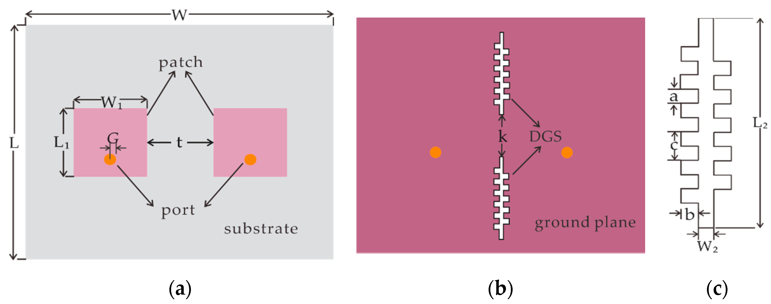
Simply, the MIMO antenna with rectangular patch structure was designed to be suitable for devices applied in the narrow band Internet of Things system, as shown in Figure 2a. There were double sides covered with thin metal copper film on the dielectric substrate board, two rectangular patches etched on one side, and the ground plane on the opposite side. The designed DGS etched on the ground plane was located at the center of the antenna patches on the opposite side, as shown in Figure 2b; and the dimensions of one zigzag unit are depicted in Figure 2c.
From Figure 2a, the structure dimensions of MIMO antenna are described as follows: The antenna consists of two microstrip antenna elements, each rectangular radiation patch with dimension L1 × W1 operate at 5.8 GHz using coaxial feeding, and the distance between patches of edge-to-edge is t. The antenna element is symmetrically printed on the dielectric substrate along the H-plane coupling. The distance from the coaxial to the antenna element, center-to-center, is G, and the inner radii of coaxial is 0.6 mm, which provides 50 Ω matching impedance. In Figure 2b, the DGS etched on the ground plane is located between two antenna elements to limit the surface wave of the elements, and two zigzag units with a gap of distance k from edge-to-edge. Figure 2c shows a zoomed-in structure of one unit, zigzag grooves on both sides of a strip with dimension of L2 × W2. Other dimensions such as a, b, and c are discussed in the next section. Both antenna patches and DGS have been etched on the polytetrafluoroethylene dielectric substrate board, with dielectric constant εr = 3.5, tangent loss σ = 0.0018, and thickness h = 1.524 mm. It can be packaged on the devices easily.

3. Simulation and Analysis of DGS

To validate the design above, an electromagnetic simulation tool, high frequency simulation software (HFSS) was used. Isolation of ports between two antenna elements and reflection coefficients of the antenna must be checked carefully.

3.1. Discussion of Different Location of One Zigzag Groove Unit

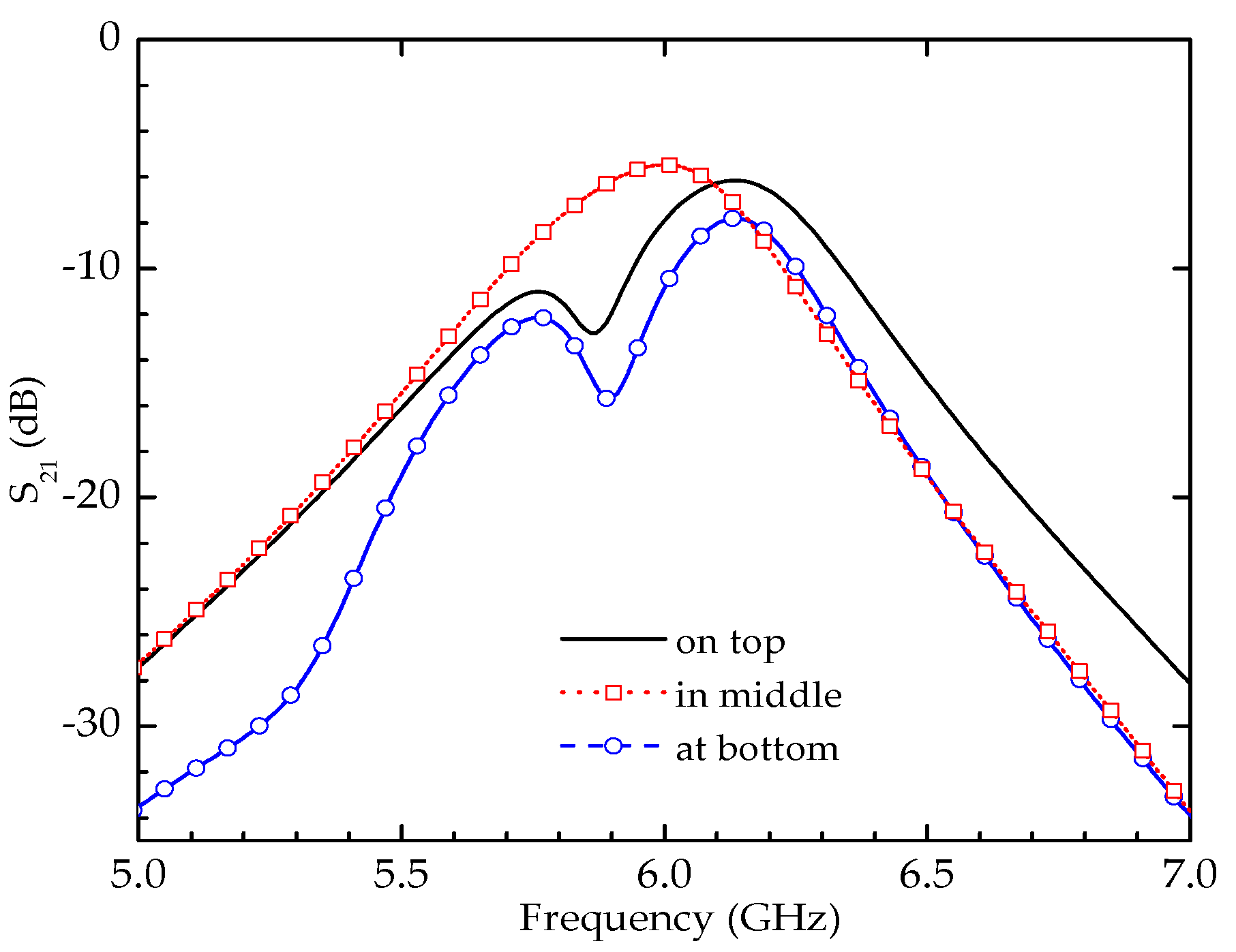
If the DGS is with one zigzag groove unit only, the location of this unit is considered first. Three typical cases are simulated to save space, which are the DGS unit located in the middle, on the top, and at the bottom positions on the ground plane side of the MIMO antenna, as shown in Figure 3. The simulated S21 is illustrated in Figure 4. As can be seen from the results of S21, when the DGS unit simulations are located at the top and bottom positions, the isolations are better than when the DGS unit was in the middle. In addition, it is clearly shown that the mutual coupling of two ports is obviously reduced around 5.8 GHz and did not live up to expectations.

3.2. Further Study of DGS

To obtain much better isolation between two antenna elements, the proposed DGS which is composed of two zigzag groove units is carried out; their locations are shown in Figure 2b. Simulated S21 is depicted in Figure 5 (with DGS). As a comparison, before the DGS is etched on the ground plane, the S21 is simulated (without DGS), also shown Figure 5. It is clear that the mutual coupling between two ports is much lower when DGS is used. The isolation is much lower with DGS than without DGS and also lower than each case in Figure 4. This result shows that the coupling of the system with DGS is 28.8 dB lower than that without DGS, which is mainly due to the fact that the DGS in array form can be effectively excited by the non-radiative aperture of microstrip antenna to change the current distribution of the ground.
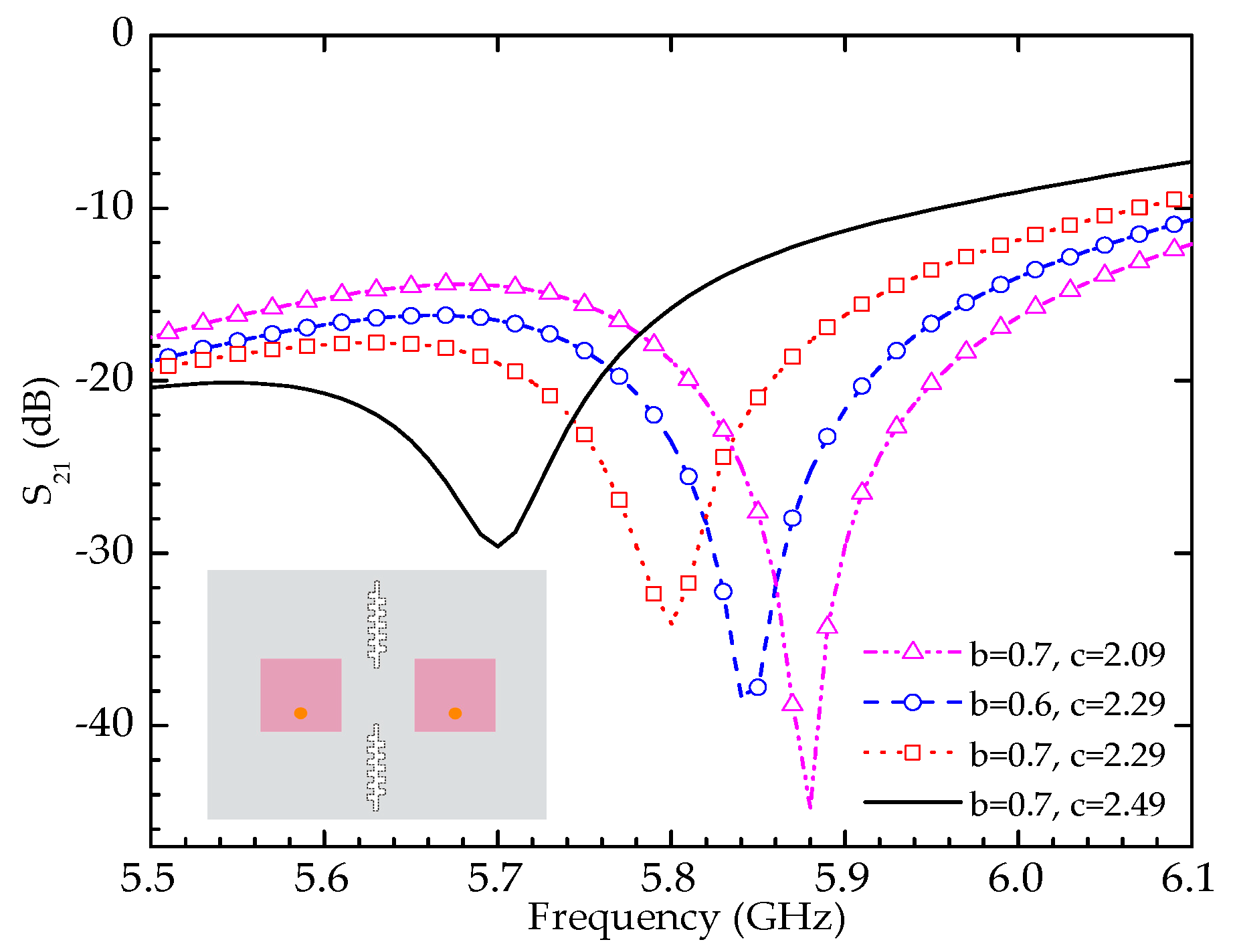
To further understand the effect of DGS on antenna performance, key parameters of DGS are carried out to analyze b, c, and k. Here, S21 is still selected as the characterization parameter. The simulated S21 is depicted, if b and c change, as shown in Figure 6, when a = 1.29, k = 1.8, L2 = 1.685, and W2 = 0.5, the DGS acts as a bandstop filter, as shown in the figure, and it shows clearly that b and c mainly influence the operating frequency of the antenna. That is, the frequency gradually shifts to lower while increasing the size of b and c, which is consistent with the description reported in [16]. In order to obtain significant isolation of two ports at 5.8 GHz, b = 0.7 and c = 2.29 are selected. The S21 curve which varies with k is simulated, as shown in Figure 7. The k mainly works on decoupling depth, meanwhile, it hardly affects the operating frequency of the bandstop filter characteristics. When the distance of two antenna elements is confirmed (2.6 mm from edge-to-edge), the effect of decoupling is best at k = 1.8. All the above default length units are millimeters.
The comparison of structure and simulation results between proposed DGS in Section 3.2 and one zigzag groove unit in Section 3.1 is shown in Figure 8 and Figure 9, respectively. As can be seen from Figure 9, the isolation of the MIMO antenna with DGS is 34.48 dB, which is 21.3 dB higher than the zigzag groove unit on the top and 17.87 dB higher than when it is at the bottom. At the same time, a center frequency of 5.8 GHz is required. Therefore, the structure composed of two zigzag groove units on the top and at the bottom are selected as the final structure.

3.3. Effect of the DGS

To understand the bandstop filter and slow wave characteristics of the DGS, the performance of the designed MIMO antenna with and without DGS has to be analyzed by using computer simulation. The working bandwidth, isolation, current distribution and gain have to be checked.
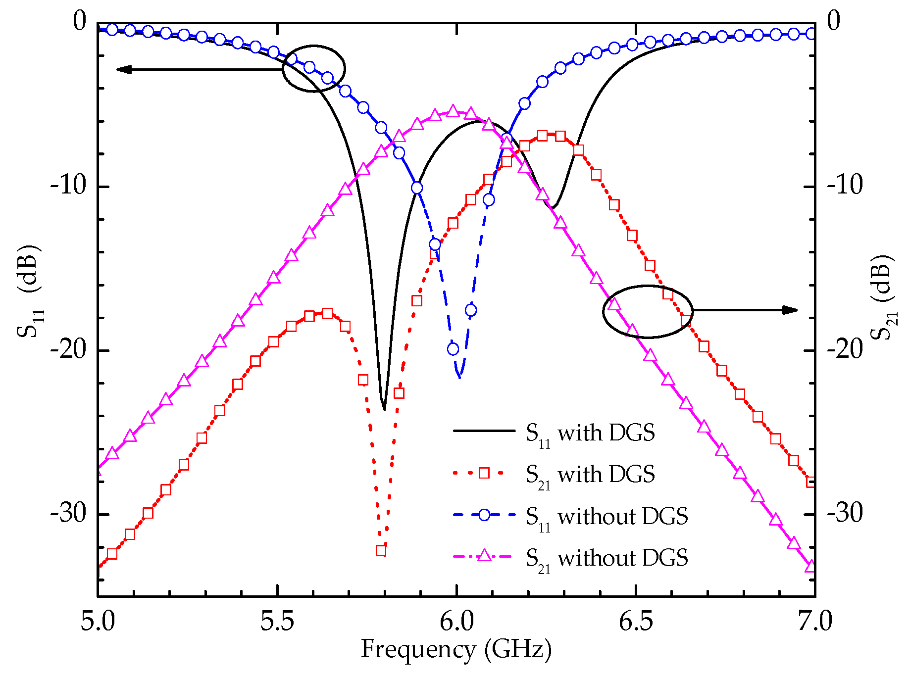
Simulation results of S11 and S21 are depicted in Figure 10. It can be seen from the figure that the working bandwidth (S11 less than −10dB) is 199 MHz (5.685–5.884 GHz), and the mutual coupling of two ports between the two antenna elements is −5.3 dB at 5.8 GHz, which results in severe H-plane coupling (it is noted that the L1 = 13.05 mm of microstrip element). Figure 10 shows the S11 and S21 of the designed MIMO antenna with DGS, and the dimensions are the same as those reported in Table 1. The operating bandwidth of the designed MIMO antenna is 170 MHz (5.722–5.892 GHz), and S21 equals −34.1 dB at a working frequency. Figure 10 shows that the working frequency of the antenna with DGS is lower than that without DGS. This is because the increased slot changed the current distribution and extended the current path effectively. Thus, the corresponding working frequency is shifted to lower. As can be seen from the Figure 11b, the current is cut off by the DGS and its path is extended. In [22] and [23], the DGS is relatively short in the antenna, therefore, the frequency almost does not change. When the DGS is added to the ground plane, additional frequency is excited, because the addition of DGS increases the effective capacitance and inductance, thus producing another operating frequency. A comparison with an antenna without a DGS shows a reduction of 0.57 mm in the size of antenna element and the isolation is improved by 28.8 dB with DGS; the impedance matching and frequency characteristic of the designed MIMO antenna are not affected, which effectively validates the effect of decoupling and the slow wave of the DGS.
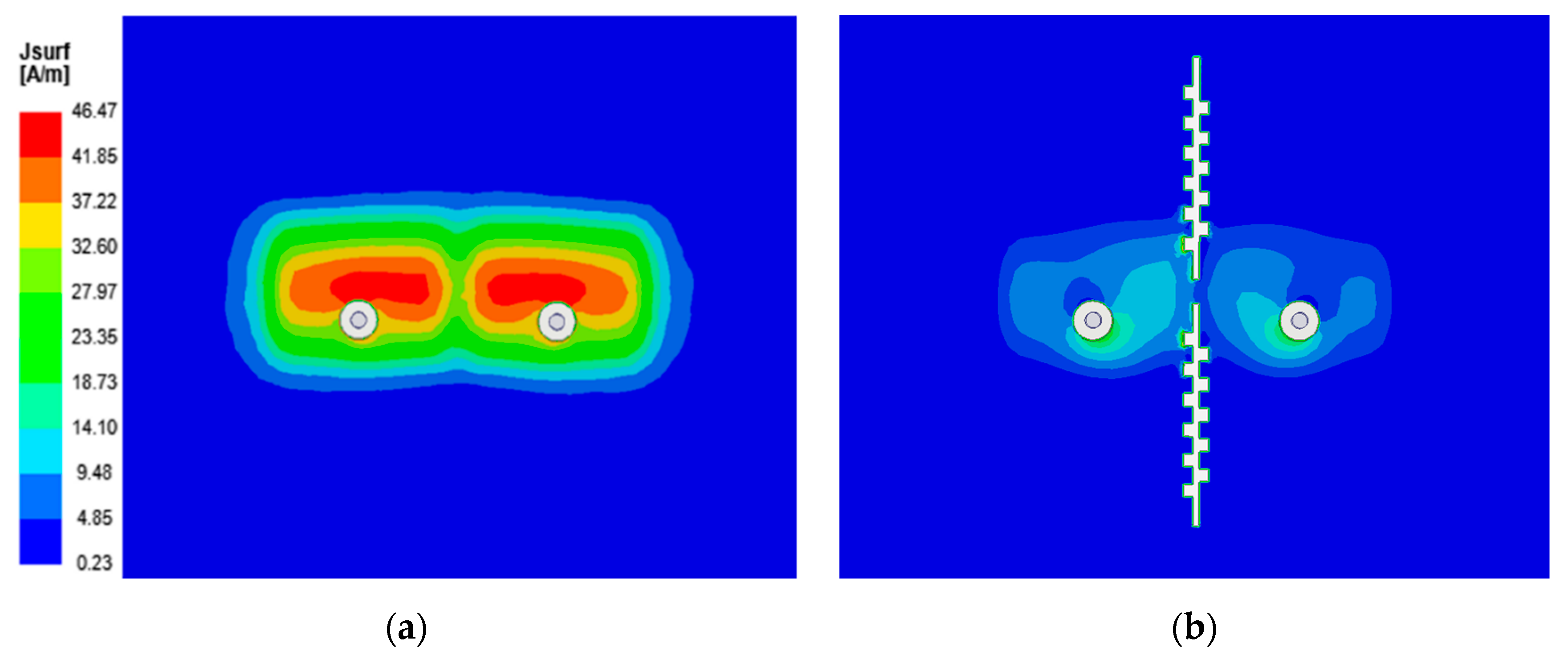
Current distribution is used to directly describe the isolation of two ports between antenna elements. Figure 11 shows the simulated current distribution of the antenna at 5.8 GHz and T/2 (T is a phase period) which is the working frequency for S11. Figure 11a shows that the currents flow to the ground plane of the other antenna element via the substrate without loading DGS. The currents which come from the other antenna element caused high coupling between the two ports. With DGS, Figure 11b shows that significant amounts of current are coupled to the DGS and radiated via DGS. As a result, the surface current density of the ground plane is obviously sparse between the two ports. Thus, the reduction of mutual coupling is achieved similar to the results shown in Figure 10.
Radiation patterns of the designed MIMO antenna are shown in Figure 12. The electric and magnetic fields are referred to E and H, respectively. Figure 12a,b shows the E plane and H plane of the radiation. It can be seen from Figure 12a that the gain is 5.06 dBi at the θ = 0° without the DGS, and the gain is 5.36 dBi at the θ = 0° after the DGS is added. We especially checked out the radiation pattern of the H-plane as compared with and without the DGS, as shown in the Figure 12b. The results do not show any difference between the main lobes’ patterns. It tells us that the DGS does not affect the radiation pattern. Whereas a considerable enhancement of the backward radiation of the designs with the planes is detected, which is mainly due to part of the radiation energy of the antenna radiating through the defected ground structure, which is inevitable. To sum up, the reduction of mutual coupling is achieved. The directional radiation can be better achieved.

4. Measurement Results and Discussion

As previously discussed, by using the electromagnetic simulation tool, HFSS, the performance of designed DGS in a MIMO antenna has been carried out, in terms of working bandwidth, reflection coefficients, mutual coupling, radiation pattern, and gain. This designed MIMO antenna with DGS was fabricated in our laboratory and must be checked in experiment. The overall size of this antenna is W × L × h = 55.6 mm × 45 mm × 1.524 mm. Other dimensions in Figure 2 and the preferred physical sizes as selected in the above discussion are listed in Table 1.
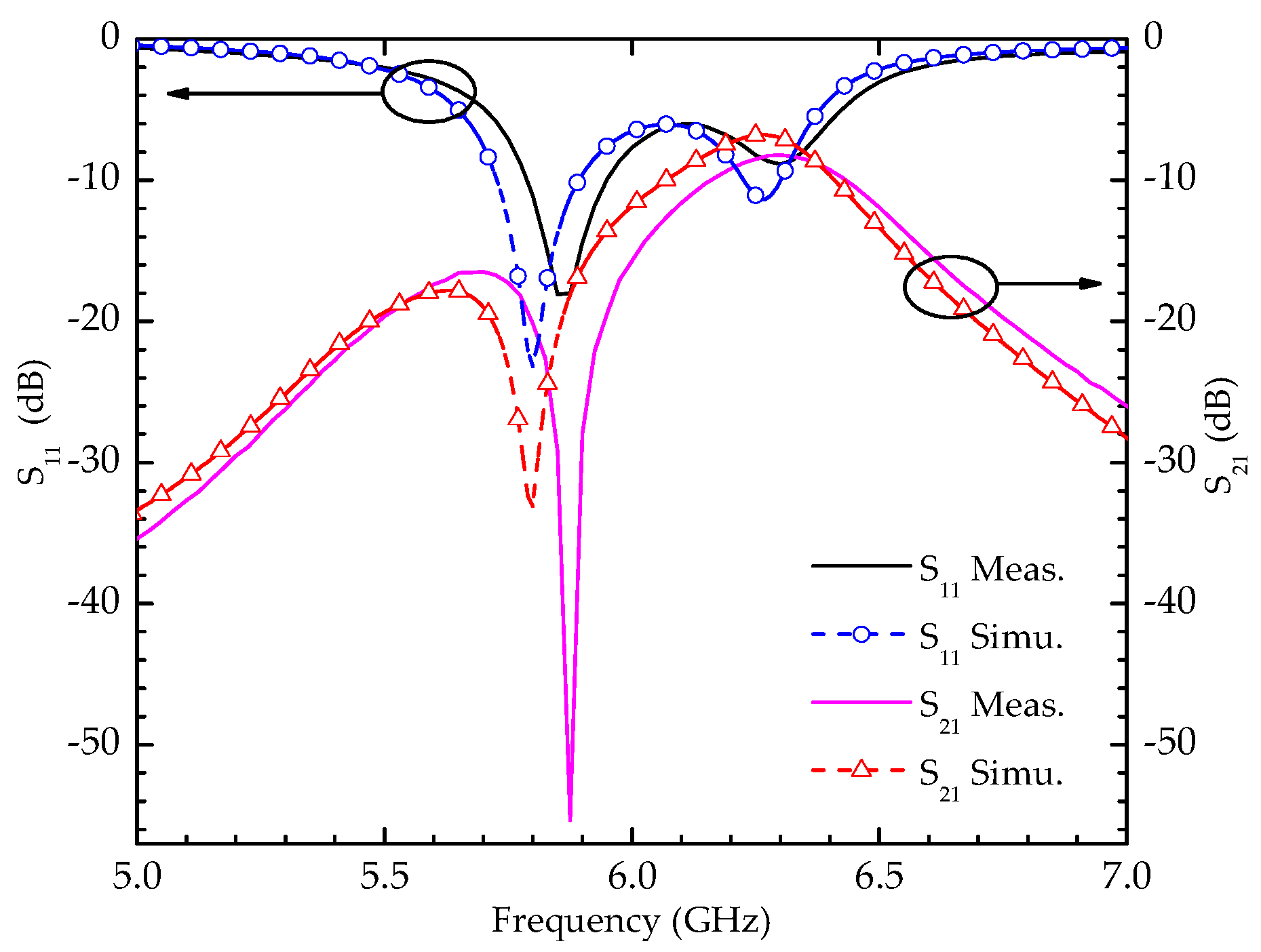
The S11 and S21 are measured by using an Agilent PNA-X network analyzer (N5244A). The results are shown in Figure 13 where solid lines represents the S parameter curve of measurement results and the imaginary lines refer to the S parameter curve of simulation results. It clearly shows that the response frequency of the measurement results fluctuations in a narrow range, in other words, the working frequency is 5.85 GHz and the operating band width is 150 MHz (5.776–5.926 GHz), which offsets to the right as compared with the simulation results. At the same time, the resonant frequency of insertion loss is 5.875 GHz and is slightly inclined to high frequency, and the isolation is −20.19 dB at 5.8 GHz, which is mainly limited by processing precision and measurement condition. To sum up, the measured results are in good agreement with the simulation, which meet the design requirements.
The ECC (ρe) is selected to characterize the correlation of the radiation pattern of the antenna elements and to evaluate the diversity gain (DG). It can be calculated by S parameters [24], as follows:
ρ e = | S 11 * S 12 + S 21 * S 22 | 2 ( 1 - ( | S 11 | 2 + | S 21 | 2 ) ) ( 1 - ( | S 22 | 2 + | S 12 | 2 ) )
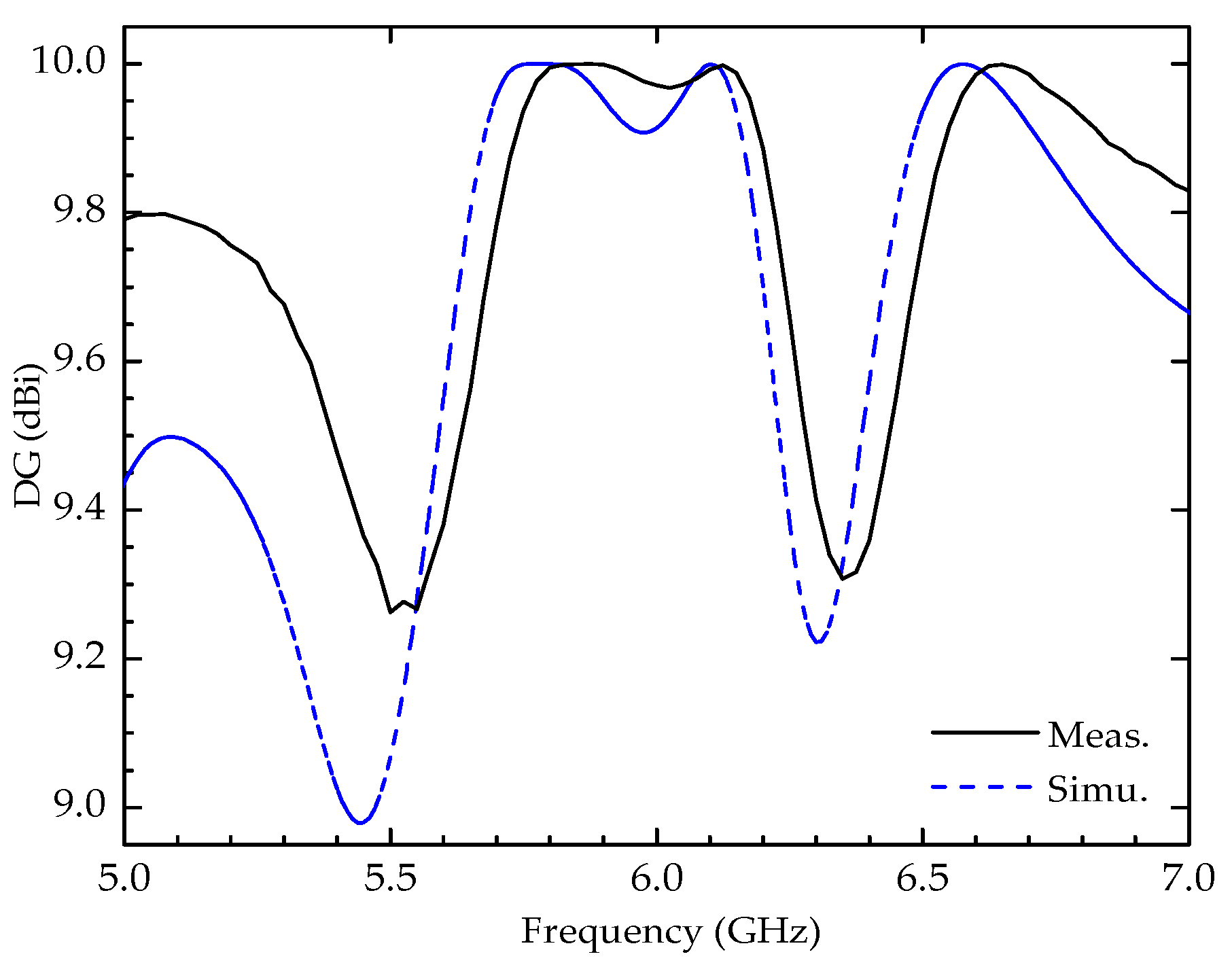
Similarly, the diversity gain is also dependent on mutual coupling (correlation), which is calculated in terms of maximum theoretical diversity gain (10 dB) by using Equation (2). The relationship between the ECC and DG is shown as the following, the lower the value of ECC is, the bigger the DG will be [1]:
DG = 10 1 - ρ e 2
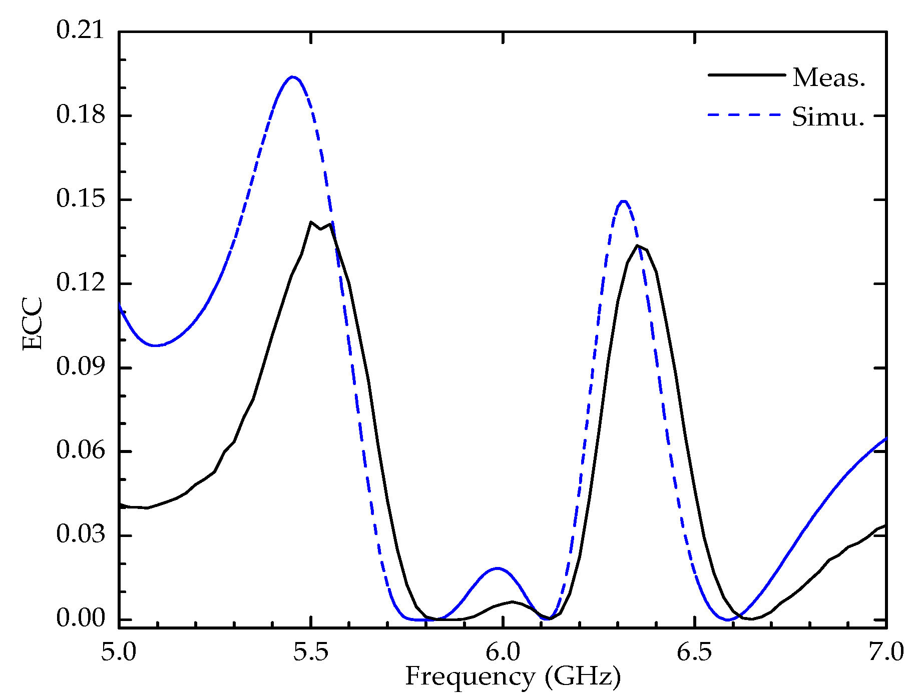
Equation (1) is used to calculate the ECC. Using the measured and simulated S parameters of the designed MIMO antenna, we calculated that ρe are lower than 0.02 and 0.05, respectively, throughout the working bandwidth. The comparison of experiment and simulation by envelope correlation coefficient is shown in Figure 14. The diversity gain of the MIMO antenna with simulated and measured results is illustrated in Figure 15. It is clear that the value of diversity gain is more than 9.952 dB and 9.873 dB throughout the whole working frequency band, respectively. Therefore, good diversity performance can be achieved.
The result of the comparison between the designed MIMO antenna and other good designs are summarized in Table 2. As a result, the designed antenna has better performance than other references listed in the Table. Considering high isolation and compactness preferentially, the microstrip antenna is not a good enough design with low reduction in the mutual coupling. The designed antenna in [4] is a good design with a high improvement in isolation, but with moderate design complexity, even high complexity. It is also interesting to note that the distance of two antenna elements (edge-to-edge) is only 0.0502 λ0 in this paper, which is very suitable for the high frequency designs.
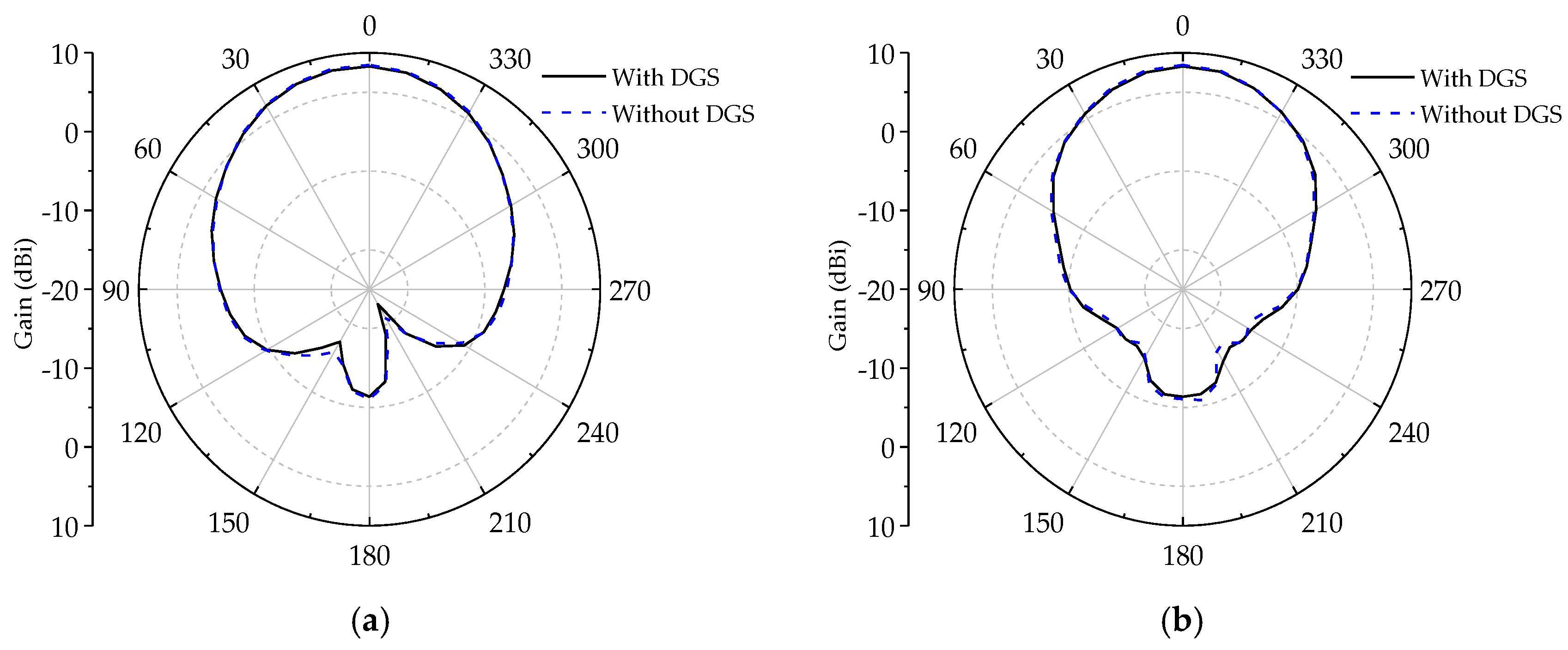
Figure 16 shows the fabricated sample of the proposed antenna in the microwave anechoic chamber in our laboratory. In order to observe more clearly, the front and back sides are zoomed in, and then put in the center of the photo. The simulated and measured results of the radiation patterns in the E and H planes are depicted in Figure 17. Simulated radiation patterns and those measured for the proposed antenna are kept consistent. Therefore, this antenna can be applied in the wireless communication systems, which works in the frequency of 5.722–5.892 GHz. The measured results of the radiation patterns are in very good agreement with the simulated results. The gain compared between measured and simulated results decreased by 1.43 dBi and 1.5 dBi, respectively, in the E and H planes. This case is mainly caused by the fabrication errors.

5. Conclusions

A compact and high isolation MIMO antenna with a small size of 45 mm × 55.6 mm × 1.524 mm is introduced successfully. The DGS is inserted into the ground plane between two ports. A very small filtering structure is obtained, and also a very high reduction in the mutual coupling of H plane is achieved. The acceptable radiation pattern and frequency characteristics and high surface current distributions with a DGS are observed clearly. The common problem of a microstrip array antenna is solved, which is hardly balanced between matching characteristics and the decoupling of the H plane. The analyses of the envelope correlation coefficient and diversity gain are presented to validate the weak correlation between antenna elements, and the simulation results are confirmed by measurement. The designed MIMO antenna is a prioritized candidate for wireless application.

Author Contributions

Design and concept, H.X., X.W., and X.A.; methodology, X.W. and H.X.; experiment, H.X.; resources, H.-x.Z.; writing—original draft preparation, X.W. and H.X.; writing—review and editing, H.-x.Z. and M.W; validation, H.-x.Z., Z.G., and M.W.; supervision, H.-x.Z., and E.L.; project administration, H.-x.Z. All authors have read and agreed to the published version of the manuscript.

Funding

This research was funded by National Natural Science Foundation of China grant number 61671200 and Key Project of Hebei Province Natural Science Foundation grant number F2017202283.

Conflicts of Interest

The authors declare no conflict of interest.

References

  1. Iram, N.; Choi, D.-Y. Study on mutual coupling reduction technique for MIMO antennas. IEEE Access 2018, 7, 563–586. [Google Scholar]
  2. Adnan, A.; Rezaul, A.; Alam, M.-M.; Islam, M.-T. A low-profile wideband antenna for WWAN/LTE applications. Electronics 2020, 9, 393. [Google Scholar]
  3. Sun, Y.; Liu, S.; Zhao, W.-M.; Cheng, Y.-X.; Lv, M.-M. Defected ground structure suppressing microstrip antenna array mutual coupling. Inf. Res. 2017, 43, 39–41+44. [Google Scholar]
  4. Habashi, A.; Nourinia, J.; Ghobadi, C. Mutual coupling reduction between very closely spaced patch antennas using low-profile folded split-ring resonators (FSRRs). IEEE Antennas Wirel. Propag. Lett. 2011, 10, 862–865. [Google Scholar] [CrossRef]
  5. Deng, J.; Li, J.; Zhao, L.; Guo, L. A dual-band inverted-F MIMO antenna with enhanced isolation for WLAN applications. IEEE Antennas Wirel. Propag. Lett. 2017, 16, 2270–2273. [Google Scholar] [CrossRef]
  6. Zhang, S.; Pedersen, G. Mutual coupling reduction for UWB MIMO antennas with a wideband neutralization line. IEEE Antennas Wirel. Propag. Lett. 2016, 15, 166–169. [Google Scholar] [CrossRef]
  7. Femina, B.-S.; Mishra, S.-K. Compact WLAN band-notched printed ultrawideband MIMO antenna with polarization diversity. Prog. Electromagn. Res. 2016, 61, 149–159. [Google Scholar] [CrossRef] [Green Version]
  8. Li, M.; Jiang, L.-J.; Kwan, L.-Y. Novel and efficient parasitic decoupling network for closely coupled antennas. IEEE Trans. Antennas Propag. 2019, 67, 3574–3585. [Google Scholar] [CrossRef]
  9. Ding, K.; Gao, C.; Qu, D.; Yin, Q. Compact broadband MIMO antenna with parasitic strip. IEEE Antennas Wirel. Propag. Lett. 2017, 16, 2349–2353. [Google Scholar] [CrossRef]
  10. Amjad, I.; Abdul, B.; Amor, S.; Mallat, N.K.; Elfergani, I.; Rodriguez, J.; Kim, S. Electromagnetic bandgap backed millimeter-wave MIMO antenna for wearable applications. IEEE Access 2019, 7, 111135–111144. [Google Scholar]
  11. Jabire, A.-H.; Zheng, H.-X.; Abdu, A.; Song, Z.-W. Characteristic mode analysis and design of wide band MIMO antenna consisting of metamaterial unit cell. Electronics 2019, 8, 68. [Google Scholar] [CrossRef] [Green Version]
  12. Lee, J.-Y.; Kim, S.-H.; Jang, J.-H. Reduction of mutual coupling in planar multiple antenna by using 1-D EBG and SRR structures. IEEE Trans. Antennas Propag. 2015, 63, 4194–4198. [Google Scholar] [CrossRef]
  13. Anitha, R.; Sarin, V.P.; Mohanan, P.; Vasudevan, K. A four-port MIMO antenna using concentric square-ring patches loaded with CSRR for high isolation. IEEE Antennas Wirel. Propag. Lett. 2015, 15, 1196–1199. [Google Scholar]
  14. Fritz-Andrade, E.; Perez-Miguel, A.; Gomez-Villanueva, R.; Jardon-Aguilar, H. Characteristic mode analysis applied to reduce the mutual coupling of a four-element patch MIMO antenna using a defected ground structure. IET Micro. Antenna Propag. 2020, 14, 215–226. [Google Scholar] [CrossRef]
  15. Mahnoor, K.; Syeda Iffat, N.; Niamat, H.; Rahman, M.; Fawad; Mirjavadi, S.S.; Khan, M.J.; Amin, Y. 4-port MIMO antenna with defected ground structure for 5G millimeter wave applications. Electronics 2020, 9, 71. [Google Scholar]
  16. Liu, Y.; Yang, X.; Jia, Y.; Guo, Y.J. A low correlation and mutual coupling MIMO antenna. IEEE Access 2019, 7, 127384–127392. [Google Scholar] [CrossRef]
  17. Ibrahim, A.-A.; Abdalla, M.-A. Compact MIMO antenna with optimized mutual coupling reduction using DGS. Int. J. Micro. Wirel. Technol. 2014, 6, 173–180. [Google Scholar] [CrossRef]
  18. Syeda, F.-J.; Akram, A. Millimetre-wave T-shaped MIMO antenna with defected ground structures for 5G cellular networks. IET Microw. Antennas Propag. 2018, 12, 672–677. [Google Scholar]
  19. Yu, Y.; Yi, L.; Liu, X. Dual-frequency two-element antenna array with suppressed mutual coupling. Int. J. Antennas Propag. 2015, 2014, 1–6. [Google Scholar] [CrossRef] [Green Version]
  20. Rifaqat, H.; Muhammad, U.-K.; Sharawi, M.S. An integrated dual MIMO antenna system with dual-function GND-plane frequency-agile antenna. IEEE Antennas Wirel. Propag. Lett. 2018, 17, 142–145. [Google Scholar]
  21. Zhao, X.-W.; Riaz, S. A dual-band frequency reconfigurable MIMO patch-slot antenna based on reconfigurable microstrip feedline. IEEE Access 2018, 6, 41450–41457. [Google Scholar] [CrossRef]
  22. Salehi, M.; Motevasselian, A.; Tavakoli, A.; Heidari, T. Mutual coupling reduction of microstrip antennas using defected ground structure. In Proceedings of the 2006 10th IEEE Singapore International Conference on Communication Systems, Singapore, 30 October–1 November 2006; pp. 1–5. [Google Scholar]
  23. Bait-Suwailam, M.M.; Siddiqui, O.F.; Ramahi, O.M. Mutual coupling reduction between microstrip patch antennas using slotted-complementary split-ring resonators. IEEE Antennas Wirel. Propag. Lett. 2010, 9, 876–878. [Google Scholar] [CrossRef]
  24. Habib, U.; Saeed Ur, R.; Cao, Q.; Khan, I.; Ullah, H. Design of SWB MIMO antenna with extremely wideband isolation. Electronics 2020, 9, 194. [Google Scholar]
Figure 1. An improved design of zigzag unit. (a) A dumbbell-shaped structure; (b) Evolved into Z-shaped structure; (c) Strung together vertically into a periodical zigzag unit.
Electronics 09 01265 g001
Figure 2. Schematic of the designed multi-input multi-output (MIMO) antenna on a double-side covered with thin metal copper film on the dielectric substrate board. (a) Two patches together with common ground plane consisting of microstrip antenna elements on front side; (b) Back side with the defected ground structure (DGS) etched on ground plane; (c) One zoomed-in zigzag unit where structure dimension marked.
Electronics 09 01265 g002
Figure 3. Different locations of the DGS unit on the ground plane side of MIMO antenna. (a) In the middle position; (b) At the top position; (c) At the bottom position, of the antenna back side, to check the isolation of two ports between antenna elements.
Electronics 09 01265 g003
Figure 4. Isolation of two ports between antenna elements for one zigzag groove unit at different locations on the back plane side, in the MIMO antenna, focus on 5.8 GHz.
Electronics 09 01265 g004
Figure 5. Isolation of the MIMO antenna without DGS and with DGS at the back plane side, focus on 5.8 GHz.
Electronics 09 01265 g005
Figure 6. Isolation at 5.8 GHz varying with different sizes of b and c when a = 1.29, k = 1.8, L2 = 1.685, and W2 = 0.5 (unit, mm).
Electronics 09 01265 g006
Figure 7. S21 on different k at 5.8 GHz where b = 0.7 and c = 2.29 (unit, mm).
Electronics 09 01265 g007
Figure 8. Proposed DGS and zigzag groove unit positions. (a) Proposed DGS; (b) Zigzag groove unit on top; (c) Zigzag groove unit at bottom.
Electronics 09 01265 g008
Figure 9. S21 of DGS and zigzag groove unit in different positions at 5.8 GHz.
Electronics 09 01265 g009
Figure 10. S11 and S21 of designed MIMO antenna with and without DGS, focus on 5.8 GHz.
Electronics 09 01265 g010
Figure 11. Current distribution of designed MIMO antenna T/2 (T is a phase period). (a) Without DGS; (b) With DGS, focus on 5.8 GHz.
Electronics 09 01265 g011
Figure 12. Operation frequency at 5.8 GHz. The radiation pattern of MIMO antenna with and without DGS. (a) E plane; (b) H plane.
Electronics 09 01265 g012
Figure 13. Measurement results compared to the simulation for the S11 and S21 of the designed MIMO antenna with DGS, focus on 5.8 GHz.
Electronics 09 01265 g013
Figure 14. Comparison of measurement and simulation by envelope correlation coefficient.
Electronics 09 01265 g014
Figure 15. Comparison of measurement and simulation by diversity gain.
Electronics 09 01265 g015
Figure 16. The photograph of fabricated sample of designed MIMO antenna together with microwave chamber and antenna measured environment, front and back sides of the antenna are zoomed in, in the photo center.
Electronics 09 01265 g016
Figure 17. At 5.8 GHz, the measured and simulated radiation pattern of the MIMO antenna. (a) E plane; (b) H plane.
Electronics 09 01265 g017
Table 1. Preferred dimension sizes of the designed MIMO antenna with DGS.
DimensionSize (mm)DimensionSize (mm)
L45k1.8
W55.6L216.85
h1.524W20.5
L112.48a1.29
W113b0.7
G2.2c2.29
t2.6--
Table 2. Comparison between this design and others in the references of the MIMO antenna.
ReferenceWorking FrequencyThe Reduction of Mutual CouplingDistance of Edge-to-EdgeDesign Complexity
[3]5.826.80.25 λ0moderate
[4]5.2300.039 λ0moderate
[16]4.9220.36 λ0high
[17]5.8130.058 λ0low
[18]31.3220.21 λ0moderate
This paper5.828.80.0502 λ0low
Note: λ0 is represented for wavelength in free space.