Article

A 100 Gb/s Quad-Lane SerDes Receiver with a PI-Based Quarter-Rate All-Digital CDR

Department of Electronic and Electrical Engineering, Hongik University, Seoul 06983, Korea
*
Author to whom correspondence should be addressed.
Electronics 2020, 9(7), 1113; https://doi.org/10.3390/electronics9071113
Submission received: 19 June 2020 / Revised: 3 July 2020 / Accepted: 5 July 2020 / Published: 9 July 2020
(This article belongs to the Special Issue Mixed-Signal VLSI Design)

Abstract

:
A 100 Gb/s quad-lane SerDes receiver with a phase-interpolator (PI)-based quarter-rate all-digital clock and data recovery (CDR) is presented. The proposed CDR utilizes a multi-phase multiplying delay-locked loop (MDLL) to generate the eight-phase reference clocks, which achieves multi-phase frequency multiplication with a small area and less power consumption. The shared MDLL generates and distributes eight-phase clocks to each CDR. The proposed CDR uses a new initial phase tracker that uses a preamble to achieve a fast lock time of about 12 ns and to provide a constant output data sequence. The CDR utilizes quarter-rate 2x-oversampling architecture, and the PI controller is designed full custom to minimize the loop latency. To improve the dithering jitter performance of the recovered clock, the decimation factor of the CDR can be adjustable. Also, a new continuous-time linear equalizer (CTLE) receiver was adopted to reduce power consumption and achieved a data rate of 25 Gb/s/lane. The proposed SerDes receiver with a digital CDR is implemented in 40 nm CMOS technology. The 100 Gb/s four-channel SerDes receiver (4 CTLEs + 4 CDRs + MDLL) occupies an active area of only 0.351 mm2 and consumes 241.8 mW, which achieves a high energy efficiency of 2.418 pJ/bit.

1. Introduction

The role of optical or electrical networks that enable high-performance servers and data centers to perform energy proportional computing [1] is increasing day by day. Therefore, there is an increasing demand for energy-efficient electrical serial links (as shown in Figure 1) that require data rates of over 25 Gb/s/lane for tera-byte computing in recent servers and data centers.
Figure 1 shows a block diagram of a typical high-speed serial-link serializer/deserializer (SerDes) architecture [2,3,4,5,6,7,8] where the transmitter (Tx) chip and the receiver (Rx) chip are connected through a backplane or copper cable channel. The serializer of Tx converts slow parallel data into high-speed serial data by using the high-frequency clock, CLKTX, generated by the phase-locked loop (PLL). The converted serial data (DATA_TX) is transmitted to the Rx chip through the lossy channel. The equalizer of the Rx chip receives the severely distorted DATA_RX signal. It compensates for the channel losses and inter-symbol interference (ISI) to generate the clock and data recovery (CDR)IN signal with an open eye. Subsequently, the clock and data recovery (CDR) uses a data sampler and a clock recovery circuit to generate the recovered data and clock from the random input data. The recovered data is then converted into slow parallel data through the deserializer. Usually, the PLL of Rx receives the low-frequency reference clock and generates the multiplied high-frequency CLKRX signal for the CDR. Conventionally, the CDR architectures have been implemented based on a PLL due to the advantage of an input jitter filtering capability. However, conventional PLL-based CDRs have a long lock time and a jitter accumulation problem [9,10]. To implement an efficient energy proportional computing network, burst-mode communication has been used for passive optical networks (PON) [11,12] and recently, an attempt has been made to increase the power efficiency by applying a burst-mode to a memory bus interface [13]. Therefore, a CDR technology having a fast lock time (= power-on time or acquisition time) is very important for low-power burst-mode implementation.
It has become common to increase data throughputs using multiple lanes (or channels) of high-speed serial links as the aggregate I/O bandwidth of a single chip exceeds hundreds of Gb/s. Among these high-speed serial buses, multi-lane source synchronous serial-links have been used for backplane applications that provide connectivity between CPU and CPU, CPU and dual in-line memory modules (DIMMs), and CPU and bridge chips. Multiple serial point-to-point lanes can be placed in parallel to increase the aggregate bandwidth. The most representative multi-lane source synchronous serial-links are Intel QuickPath Interconnect (QPI) [14] and AMD HyperTransport (HT) [15]. Figure 2 shows typical multi-lane high-speed source synchronous serial-link architectures [16]. As shown in Figure 2a, in the source synchronous clocking structure, the Rx receiver uses the transmitted clock almost identically correlated to the noise environment of the Tx chip so that high-speed data can be restored with low power and low latency. If half-rate sampling is used on the Rx chip, the frequency of the transmitted clock can be lowered to half.
As the data rate of the channel increases above a few Gb/s/lane, the method of Figure 2a has reached its limit, and as shown in Figure 2b, PLL (or DLL or just simple deskew circuits) has been added to the clock path at the Rx side, through which improved timing margin and skew cancellation [17,18,19,20,21]. If 1:2 de-multiplexing is used at the receiver path of each data lane, the forwarded clock rate can be reduced to 1/2 frequency.
As shown in Figure 2c, as the data rate increases above about 10 Gb/s/lane, CDR and equalizer circuits are added to each data lane to improve signal integrity and provide much higher communication bandwidth [5,22,23,24,25,26,27,28]. However, these conventional multi-lane receivers with CDRs [5,22,23,28] generally have the disadvantages of a large area and high-power consumption. In particular, these multi-lane receivers have a problem that it is difficult to apply to burst mode applications due to the large CDR lock time. In particular, since [5,22,23] all use a PLL as a high-frequency clock generator, there are issues such as a very long lock time, jitter peaking, and jitter accumulation problems that may degrade the CDR performance. Among the various CDR architectures, phase interpolator (PI)-based digital CDRs offer a fast lock time with better jitter performance [5,6,29,30,31,32].
In this paper, a new 100 Gb/s quad-lane SerDes receiver with a small area and low-power consumption is presented. The proposed all-digital quarter-rate PI-based CDR utilizes a multiplying delay-locked loop (MDLL) instead of the usual PLL to generate the eight-phase high-frequency clocks required for the PI operation [24,33]. Through this, both frequency multiplication and eight-phase clock generation are performed at the same time, thereby achieving an area and power reduction and low-jitter characteristics. The proposed digital CDR uses a new initial phase tracker that uses a preamble to reduce the lock time. The CDR utilizes a quarter-rate 2x-oversampling architecture, and the PI controller is designed full custom to minimize the loop latency. The update rate of the CDR can be adjustable, resulting in an improved peak-to-peak (p-p) clock jitter performance. As a result, it has the advantage of having a fast lock time of about 12 ns and a constant output data sequence. Moreover, a new differential near-ground receiver with an adaptive continuous-time linear equalizer (CTLE) was adopted to reduce the power consumption and ensure high-frequency characteristics up to 25 Gb/s/lane.
The rest of this paper is organized as follows. Section 2 presents the architecture and operation of the proposed quad-lane SerDes Receiver and the quarter-rate CDR. Section 3 shows the experimental results and Section 4 presents the conclusion.

2. Proposed Multi-Lane SerDes Receiver Architecture

The proposed SerDes link is for the duplex interface structure with four data lanes and one clock lane. Figure 3 shows a block diagram of the proposed 100 Gb/s quad-lane (25 Gb/s/lane × 4 differential lanes) SerDes receiver architecture. Here, it is assumed that a forwarded clock in which a low-frequency clock (= 625 MHz) is transmitted through a separate differential lane without equalization, so the tracking of a data jitter in a wide frequency range is possible. The multi-lane interface architecture presented in this paper is based on source synchronous clocking. Moreover, the proposed CDR structure can be applied to plesiochronous systems in which the Tx and the Rx use separate independent low-frequency quartz-based reference clocks.
The proposed SerDes receiver core consists of a shared multi-phase MDLL, an all-digital PI-based quarter-rate CDR, and a CTLE. The shared MDLL receives a 625 MHz reference clock and provides eight-phase (= p0~p7) quarter-rate (= 6.25 GHz) clocks multiplied by ten times (n = 10) and distributes them to each CDR block. The use of the proposed multi-phase MDLL has the advantage of the area and power reduction by simultaneously performing frequency multiplication and multi-phase clock generation. The CTLE is designed to compensate for a channel loss of about 19.7 dB at 12.5 GHz. The channel loss of the 40 cm transmission line used in this paper is about 22.6 dB at 12.5 GHz. This channel loss value is similar to those shown by a typical chip-to-chip and midrange backplane interface below 50 cm long [30]. The proposed CDR includes four data samplers and four edge samplers, and performs a 1-to-4 de-multiplexing operation at a quarter-rate using a 2x-oversampling technology. A total of eight samplers (four corresponding to the data samples and four corresponding to the edge samples) recover 6.25 Gb/s four-bit parallel data (D<3:0>) and four 6.25 GHz clocks (Dclk0~Dclk 3) from 25 Gb/s random data input through the CTLE. To perform this operation, this CDR includes a phase interpolator (PI), a phase selector (PS), and a PI controller to provide phase-adjusted driving clocks for each data sampler and an edge sampler. In particular, a new initial phase tracker inside the PI controller is used to speed up the lock time and to provide a constant data output sequence. Detailed CDR configuration and operation are described in the following section.

2.1. Proposed All-Digital PI-Based Quarter-Rate CDR Architecture

Figure 4a shows the block diagram of the proposed all-digital 25 Gb/s PI-based quarter-rate CDR architecture. The CDR is composed of four data samplers, four edge samplers, four phase selectors (PS), four phase interpolators (PI), and a PI controller. The proposed CDR adopts a quarter-rate architecture to sufficiently widen the timing margin of the input sampler and to simplify the clock distribution network with much a lower sampling clock frequency. To this end, four data samplers (#1~#4) are arranged in parallel on the input stage, and the four data samplers are operated in synchronization with four Dclks (Dclk0~Dclk3) operating at quarter-rate (= 6.25 GHz), respectively. Additionally, 2x-oversampling technology is used to find the transition position of the input data stream. To this end, four edge samplers operating at quarter-rate are arranged parallel to the input. As shown in Figure 4b, when the CDR is locked, the four data clocks (Dclk0~Dclk3) are aligned to the middle of each output data (D<0>~D<3>), respectively. For this operation, the PI controller generates the MA<1:0>, MB<1:0>, and PI<8:0> signals to control the PS and PI. The PS and PI generate the four Dclks (Dclk0~Dclk3) required for the four data samplers, and the adjacent Dclks are out of phase with each other by 90 degrees. The PS and PI also generate the four Eclks (Eclk0~Eclk3) required for the four edge samplers.
By applying this 2x-oversampling quarter-rate CDR technology, demultiplexed 4-bit parallel data (D<3:0>) can be restored from the 25 Gb/s serial random input data. This CDR structure has the advantage that the order of the recovered 4-bit parallel data (D<3:0>) is always constant. This means, for instance, that the data sampler #1 clocked with Dclk0 always outputs D<0> first, and the data sampler #2 clocked with Dclk1 always outputs D<1> first. This function is performed through the PI controller with the initial tracking mode.
On the other hand, the order of the 4-bit parallel data output by the conventional quarter-rate CDR with 1:4 demultiplexing may not be constant. This means that in the conventional method, the data sampler #1 can output any data from D<0> to D<3> first. Thus, the conventional quarter-rate CDRs may require additional reordering circuits to set the order of the parallel data stream that is randomly output, which can have the disadvantage of increasing the latency and area overhead. In a packet protocol-based serial interface, the order of deserialized data can be arranged in a training mode with an additional preamble overhead of increased latency.

2.2. Proposed PI Controller

Figure 5a shows the block diagram of the proposed PI controller. It consists of an initial phase tracker (IPT), an early/late (E/L) detector, a majority vote logic (MVL), a digital loop filter (DLF), a 2-to-1 MUX, and an octant phase controller. The proposed PI controller provides two operation modes; initial tracking mode and sequential tracking mode.
At power-on, the operation of the CDR starts in the initial tracking mode. The IPT uses a repeated preamble of the “00001111” pattern to achieve both the fast lock time and the constant data output sequence. During this mode, the IPT compares E<1> and E<3> edge information based on the phase of Eclk1. The PI controller quickly makes the rising edge of Eclk3 align with the first rising edge of the “1111” pattern. Since the phases of Eclk1 and Eclk3 are shifted 180 degrees, when the rising edge of Eclk3 is located at the center of the preamble “00001111” pattern, Dclk1 is automatically located at the center of D0 as shown in Figure 4b and Figure 5a. In this initial tracking mode, the operation of the CDR is similar to the phase tracking operation of a delay-locked loop (DLL). The initial tracking mode is performed during 36 CLKCONT cycles. The stop signal changes from zero to one after 36 CLKCONT cycles. The frequency of CLKCONT (fCLKcont) is 3.125 GHz, which is half of the frequency of Eclk3, so the total initial tracking mode takes about 11.52 ns.
The PI of the PI-based CDR must have the ability to randomly shift the phase of the output signal up to 360 degrees. Therefore, as shown in Figure 5b, the output signals MA<1:0> and MB<1:0> of the octant phase controller are used to allocate the octant phase planes. The PI<8:0> is used to divide the 45 degree phase into nine phases, so the resolution of the proposed PI corresponds to 5 degrees, which is about 2.22 ps in this design. Thus, the octant phase planes consist of a total of 72 phase steps, which are associated with an initial tracking mode of only 36 (= 72/2) cycles (for 180 degrees in both directions).
After the initial tracking mode, the sequential tracking mode using 2x-oversampling is performed. The output of the eight samplers, D<3:0> and E<3:0>, are used as an input to the E/L detector. The E/L detector compares the output of adjacent samplers and generates the Early<7:0> and Late<7:0> signals. The MVL determines whether the phases of the sampling clocks are earlier or later than the incoming data stream by majority voting. The digital loop filter (DLF) composed of an encoder and a variable finite-state machine (FSM) receives the EA<1:0> and LA<1:0> signals. It generates the UPDLF/DNDLF signals that can change the output signals of the octant phase controller. The encoder compares the EA<1:0> and LA<1:0> to generate the Comp signal and the Equal signal. If EA<1:0> has more numbers than LA<1:0>, the output Comp signal goes high, and in the opposite case, the Comp signal goes low. If E<1:0> and L<1:0> have the same number of 1′s, an Equal signal is generated, and the FSM maintains the previous value. The octant phase controller implemented with an up/down counter generates the control codes (MA<1:0>, MB<1:0>, and PI<8:0>) for the phase selector (PS) and the phase interpolator (PI). For the design of the proposed PI controller, a full-custom design was used for a high-speed operation. Both the E/L detector and the IPT operate at 6.25 GHz. Other PI controller blocks also operate at a high speed of 3.125 GHz, which results in the advantage of reducing the loop latency.
As the update rate of the CDR increases, the input jitter tolerance improves, whereas the dithering jitter of the recovered clock deteriorates. The jitter tolerance refers to the ability of the CDR to maintain the targeted bit error rate (BER) when a low-frequency input sinusoidal jitter (usually from a few kHz to tens of MHz) is added and injected into the input data of the CDR. In applications that do not require spread-spectrum clocking, the BER can be minimized by paying more attention to jitter generation than jitter tolerance. Therefore, it is necessary to have the ability to adjust the update rate of the CDR depending on the application field of the CDR.
In this paper, to reduce the dithering jitter of the recovered clock and prevent the BER increase, the FSM of the proposed DLF performs a decimation filter [6] function. When the decimation factor (DF) control (DFCONT) signal is 0, the FSM operates as a four-state machine and outputs once when four consecutive Comp impulses occur. Thus, the update rate of the CDR is fCLKcont × DF, where DF = 1/4. When the DF is 1, the FSM operates in eight states, and the update rate of the CDR becomes fCLKcont/8 with DF = 1/8, which has the effect that the dithering jitter is further reduced.
Figure 6 shows the Early/Late (E/L) detector, which consists of four bang-bang phase detectors (PD), four de-multiplexers (DEMUX), and one 1/2 divider. When the sequential tracking mode starts after the initial tracking mode ends, the four bang-bang PDs using the Alexander equation [34] generate the L0–L3 and E0–E3 signals. After going through the four DEMUX blocks, the Early<7:0> and Late<7:0> signals are generated.

2.3. Proposed CTLE

Figure 7 shows the block diagram of the proposed CTLE, which consists of a near-ground (NG) receiver [35,36], an adaptive CTLE, and a power detector [37]. High-speed small-swing differential input signals (RXIN, RXINb) passing through the parasitic RLC input network (including package/bond wire/PAD and electrostatic discharge (ESD) devices) are applied as inputs to the NG receiver.
The NG receiver adopts a dual gain-path common-gate amplifier with feed-forward capacitors (CFF) that boost high-frequency gain. The NG receiver also utilizes an adaptive bias generator (ABG) to compensate for the input common-mode variation and to improve the channel impedance matching performance. The input terminal of the NG receiver provides the impedance matching function for the channel termination, which has the advantage of not requiring additional channel termination devices. If the amplitude of the high-speed serial input signal changes, the characteristics of the NG receiver and impedance matching are affected. The ABG using common-mode feedback can reduce the current mismatch problem in the receiver input stage according to the VCM level changes, which results in improved impedance matching performances. The PMOS active inductor loads of the NG receiver provide efficient high-frequency compensation with less area and power consumption than the passive inductor loads.
The proposed adaptive CTLE is a two-stage differential pair amplifier with active inductor loads. It is used to compensate for the additional high-frequency gain at about 12.5 GHz to generate open-eye data (CDRIN, CDRINb). The power detector [37] using the spectrum balancing technique creates a control voltage (VCTRL) that can adaptively adjust the gain of the CTLE. The power detector consists of a high-pass filter (HPF), a low-pass filter (LPF), a rectifier, and a voltage-to-current converter. Figure 8 shows the simulated frequency response of the proposed CTLE for different VCTRL voltages. The proposed CTLE achieves a maximum gain boosting characteristic of about 19.7 dB at a Nyquist frequency of 12.5 GHz.

2.4. Proposed Multi-Phase MDLL

Figure 9 shows the block diagram of the multi-phase multiplying delay-locked loop (MDLL) [38,39] used in this paper. The proposed multi-phase MDLL consists of a phase detector (PD), a charge pump (CP), a loop filter (LF), a voltage controlled delay line (VCDL), a divide-by-10 divider, and a select logic. The MDLL uses a four-stage differential delay line to generate eight-phase clocks (p0 to p7), each with a phase difference of 45 degrees. The proposed MDLL generates 6.25 GHz eight-phase clocks multiplied by ten times using a reference clock of 625 MHz. The lock time of the MDLL is about 350 ns. The proposed MDLL consumes about 24.2 mW of power at 6.25 GHz and achieves a peak-to-peak (p–p) jitter of 10.5 ps. The active area of the proposed MDLL is only 170 μm × 80 μm. The MDLL core consumes 19.7 mW, and the multi-phase clock distribution across the four CDRs consumes about 4.5 mW. The shared MDLL is located in the center of the four CDRs to minimize the length of the clock distribution. The clock distribution of multi-phase high-frequency clocks is a critical task due to problems such as noise coupling, clock skew, and the power consumption of the clock tree. However, since the overall size of the proposed quad-lane receiver architecture is very small and the clock distribution length in one direction is shorter than 230 μm, noise coupling and power consumption increase problems can be minimized.

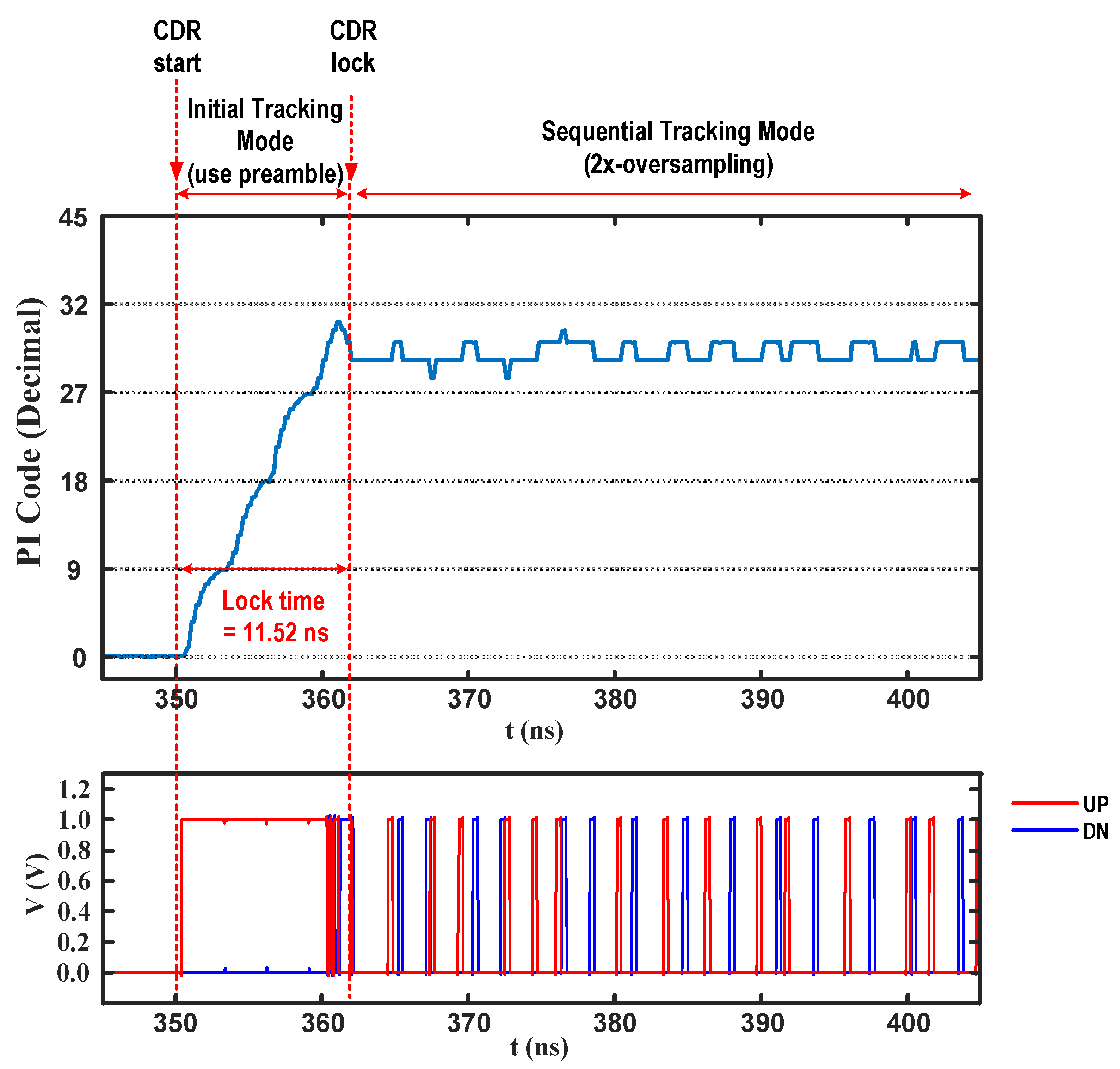
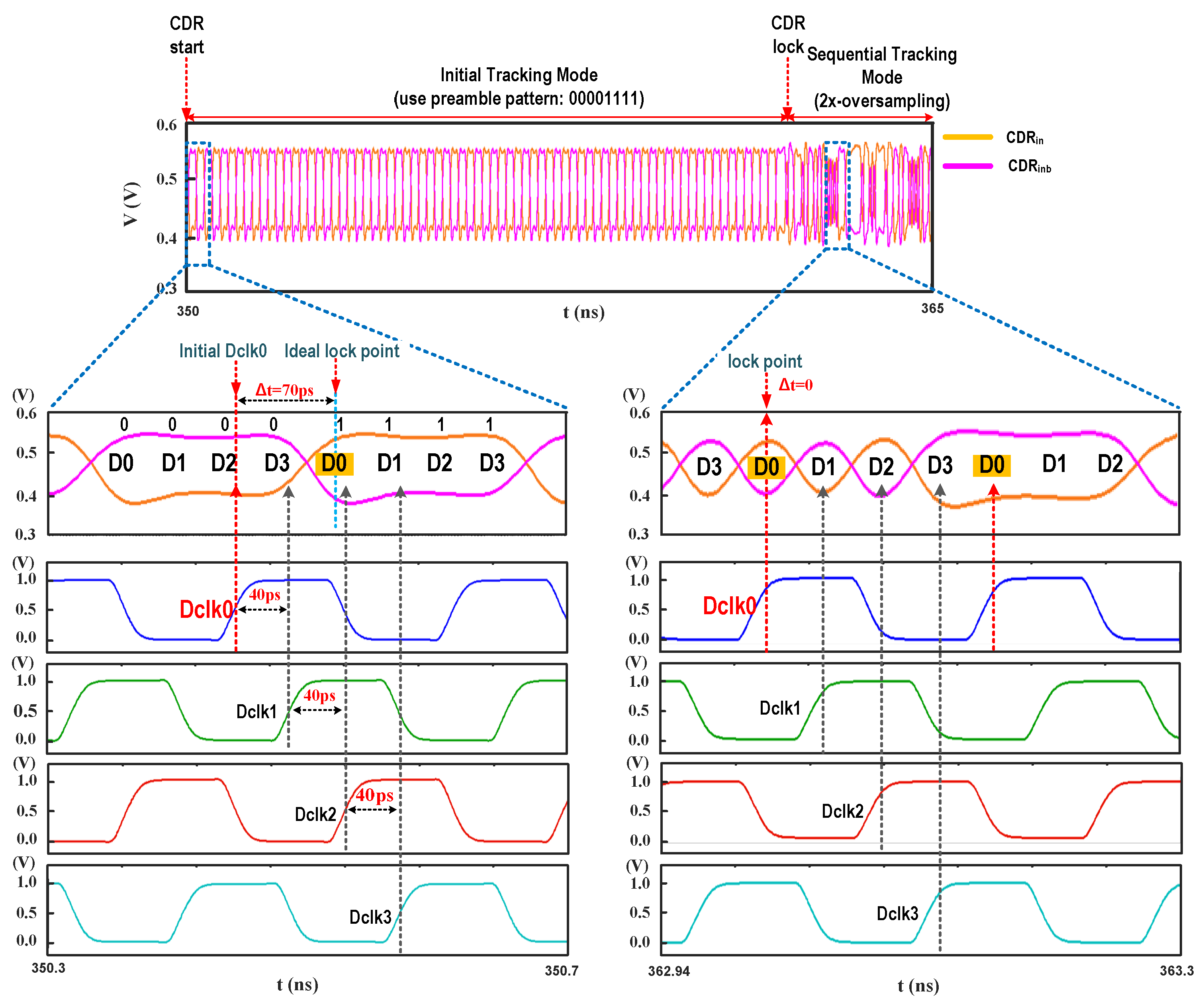
3. Experimental Results

The proposed 100 Gb/s quad-lane SerDes receiver was implemented in a 40 nm CMOS process. Figure 10 shows the layout of the quad-lane SerDes receiver composed of four CTLEs, one shared MDLL, and four CDRs. The total active area of the quad-lane SerDes receiver is only 780 μm × 450 μm (= 0.351 mm2). To achieve an aggregate data rate of 100 Gb/s, the proposed four-channel SerDes receiver consumes a total power of 241.8 mW (MDLL = 24.2 mW, CTLE × 4ea = 81.6 mW, CDR × 4ea = 136 mW), which results in a high-energy efficiency of 2.418 pJ/bit.
Figure 11 shows the locking process of the proposed 25 Gb/s/lane quarter-rate all-digital CDR. When the CDR is activated, the initial tracking mode operates for 36 CLKcont cycles by using a repeated preamble of the “00001111” pattern to achieve a fast acquisition time and a constant data output sequence, where the CDR update rate is 3.125 GHz (= 0.32 ns). When the initial tracking mode is completed, and the DATA#1 output is synchronized to Dclk0, then the CDR enters the sequential tracking mode and performs 2x-oversampling. By controlling the decimation factor of the DLF, the CDR update rate can be adjusted to have fCLKcont/4 or fCLKcont/8 to minimize the dithering jitter. As shown in Figure 11, the lock time of the proposed CDR is only less than 12 ns.
Figure 12 shows the simulated locking process of the proposed CDR at 25 Gb/s/lane. When the CDR starts, the phase error (Δt) between the Dclk0 and the ideal lock point is about 70 ps. After the initial tracking mode using the preamble data pattern is finished, it can be confirmed that the phase error Δt becomes zero, and the CDR input D0 is synchronized to Dclk0.
Figure 13 left shows the simulated eye diagram of the CTLE input when the channel loss is about 22.6 dB at 12.5 GHz, where the input data eye is completely closed. Figure 13 right shows the simulated eye diagram at the CTLE output operating at 25 Gb/s with a 231−1 pseudorandom bit stream (PRBS) data pattern, where the data eye is opened with 0.67 unit interval (UI) (= 27 ps).
Figure 14 shows the eye diagram of the recovered quarter-rate 6.25 GHz clock (Dclk0), which has a p–p jitter of 18 ps and a root mean square (RMS) jitter of 3.5 ps, respectively, when DF = 1/4. When DF = 1/8, it shows an improved p–p jitter of 16.5 ps and an RMS jitter of 3.5 ps, respectively. Figure 15 shows the eye diagram of the recovered quarter-rate 6.25 Gb/s data, which has a p–p jitter of 22 ps and an RMS jitter of 3.7 ps, respectively, when DF = 1/4. When DF = 1/8, it shows a p–p jitter of 20.5 ps and an RMS jitter of 3.6 ps, respectively.
Table 1 summarizes the performance of the proposed all-digital CDR with the state-of-the-art PI-based CDRs. The results in this work are the post-layout simulation values. It can be confirmed that the proposed CDR has the best energy efficiency of 2.34 pJ/bit (= 2.34 mW/Gb/s). Additionally, Ref. [29,32] require a high-frequency clock generator of 10 GHz or higher as an external reference clock source. This means that the use of an additional PLL circuit, which has the disadvantage of power consumption and silicon area increase.
Table 2 provides a comparison between this work and some recently published multi-lane SerDes receiver chips. It can be confirmed that the proposed quad-channel SerDes receiver (4 CTLEs + 4 CDRs + 1 MDLL) achieves the highest energy efficiency of 2.418 pJ/bit and the highest data rate of 25 Gb/s/channel, while using a small area of only 0.351 mm2.

4. Conclusions

We have presented an energy-efficient, small-area 100 Gb/s quad-lane SerDes receiver with a PI-based quarter-rate all-digital CDR. The proposed PI-based CDR utilizes a multi-phase MDLL to achieve lower clock jitter, a smaller area, and a lower power consumption. The proposed digital CDR uses a new preamble-based initial tracking mode to achieve a fast lock time of less than 12 ns, which is suitable for use in burst-mode applications. The CDR uses a quarter-rate 2x-oversampling architecture and a new full custom PI controller with an adjustable update rate, resulting in a reduced dithering jitter. A new small-area low-power CTLE using an NG receiver was adopted to achieve a data rate of 25 Gb/s/lane. Implemented in 40 nm CMOS technology, the four-channel SerDes receiver achieves an aggregate data rate of 100 Gb/s and occupies an active core area of only 0.351 mm2. It consumes only 241.8 mW and achieves a high energy efficiency of 2.418 pJ/bit.

Author Contributions

Conceptualization, J.K.; methodology, H.H.; validation, J.K. and H.H.; formal analysis, H.H.; investigation, J.K and H.H.; data curation, H.H.; writing—original draft preparation, J.K and H.H.; writing—review and editing, J.K.; supervision, J.K.; project administration, J.K.; funding acquisition, J.K. All authors have read and agreed to the published version of the manuscript.

Funding

This research was funded and conducted under “the Competency Development Program for Industry Specialists” of the Korean Ministry of Trade, Industry and Energy (MOTIE), operated by Korea Institute for Advancement of Technology (KIAT). (No. N0001883, HRD program for N0001883). This work was also supported by National Research Foundation of Korea (NRF 2019R1A2C-1010017). The EDA tools were supported by IDEC.

Conflicts of Interest

The authors declare no conflict of interest.

References

  1. Barroso, L.A.; Holzle, U. The case for energy-proportional computing. Computer 2008, 40, 33–37. [Google Scholar] [CrossRef]
  2. Chen, S.; Li, H.; Chiang, P.Y. A robust energy/area-efficient forwarded-clock receiver with all-digital clock and data recovery in 28-nm CMOS for high-density interconnects. IEEE Trans. Very Large Scale Integr. (VLSI) Syst. 2016, 24, 578–586. [Google Scholar] [CrossRef]
  3. Guo, S.; Liu, T.; Zhang, T.; Xi, T.; Wu, G.; Gui, P.; Fan, Y.; Maung, W.; Morgan, M. A low-voltage low-power 25 Gb/s clock and data recovery with equalizer in 65 nm CMOS. In Proceedings of the 2015 IEEE Radio Frequency Integrated Circuits Symposium (RFIC), Phoenix, AZ, USA, 17–19 May 2015; pp. 307–310. [Google Scholar]
  4. Chung, S.H.; Kim, L.S. 1.22 mW/Gb/s 9.6 Gb/s data jitter mixing forwarded-clock receiver robust against power noise with 1.92 ns latency mismatch between data and clock in 65 nm CMOS. In Proceedings of the 2012 Symposium on VLSI Circuit (VLSIC), Honolulu, HI, USA, 13–15 June 2012; pp. 144–145. [Google Scholar]
  5. Kalantari, N.; Buckwalter, J.F. A multichannel serial link receiver with dual-loop clock-and-data recovery and channel equalization. IEEE Trans. Circuits Syst. I Regul. Pap. 2014, 60, 2920–2931. [Google Scholar] [CrossRef]
  6. Wu, G.; Huang, D.; Li, J.; Gui, P.; Liu, T.; Guo, S.; Wang, R.; Fan, Y.; Chakraborty, S.; Morgan, M. A 1-16 Gb/s all-digital clock and data recovery with a wideband high-linearity phase interpolator. IEEE Trans. Very Large Scale Integr. (VLSI) Syst. 2016, 24, 2511–2520. [Google Scholar] [CrossRef]
  7. Kwak, Y.H.; Kim, Y.; Hwang, S.; Kim, C. A 20 Gb/s clock and data recovery with a ping-pong delay line for unlimited phase shifting in 65 nm CMOS process. IEEE Trans. Circuits Syst. I: Regul. Pap. 2013, 60, 303–313. [Google Scholar] [CrossRef]
  8. Bueren, G.V.; Rodoni, L.; Jaeckel, H.; Brun, R.; Holzer, D.; Huber, A.; Schmatz, M. 5.75 to 44Gb/s quarter rate CDR with data rate selection in 90 nm bulk CMOS. In Proceedings of the ESSCIRC 2008—34th European Solid-State Circuit Conference, Edinburgh, UK, 15–19 September 2008; pp. 166–169. [Google Scholar]
  9. Hsieh, M.T.; Sobelman, G.E. Architectures for multi-gigabit wire-linked clock and data recovery. IEEE Circuits Syst. Mag. 2008, 8, 45–57. [Google Scholar] [CrossRef]
  10. Choi, W.S.; Anand, T.; Shu, G.; Elshazly, A.; Hanumolu, P.K. A burst-mode digital receiver with programmable input jitter filtering for energy proportional links. IEEE J. Solid-State Circuits 2015, 50, 737–748. [Google Scholar] [CrossRef]
  11. Su, C.; Chen, L.K.; Cheung, K.W. Theory of burst-mode receiver and its applications in optical multiaccess networks. J. Lightwave Technol. 1997, 15, 590–606. [Google Scholar]
  12. Verbeke, M.; Rombouts, P.; Ramon, H.; Verbist, J.; Bauwelinck, J.; Yin, X.; Torfs, G. A 25 Gb/s all-digital clock and data recovery circuit for burst-mode applications in PONs. J. Lightwave Technol. 2018, 36, 1503–1509. [Google Scholar] [CrossRef] [Green Version]
  13. Leibowitz, B.; Palmer, R.; Poulton, J.; Frans, Y.; Li, S.; Wilson, J.; Bucher, M.; Fuller, A.M.; Eyles, J.; Aleksic, M.; et al. A 4.3 GB/s mobile memory interface with power-efficient bandwidth scaling. IEEE J. Solid-State Circuits 2010, 45, 889–898. [Google Scholar] [CrossRef]
  14. Ziakas, D.; Baum, A.; Maddox, R.; Safranek, R. Intel® QuickPath interconnect architectural features supporting scalable system architectures. In Proceedings of the 18th IEEE Symposium on High Performance Interconnects, Mountain View, CA, USA, 18–20 August 2010; pp. 1–6. [Google Scholar]
  15. Loke, A.; Doyle, B.; Maheshwari, S.; Fischette, D.; Wang, C.; Wee, T.; Fang, E.S. An 8.0-Gb/s HyperTransport transceiver for 32-nm SOI-CMOS server processors. IEEE J. Solid-State Circuits 2012, 47, 2627–2642. [Google Scholar] [CrossRef]
  16. Zerbe, J.; Daly, B.; Luo, L.; Stonecypher, W.; Dettloff, W.; Eble, J.C.; Stone, T.; Ren, J.; Leibowitz, B.; Bucher, M.; et al. A 5 Gb/s link with matched source synchronous and common-mode clocking techniques. IEEE J. Solid-State Circuits 2011, 46, 974–985. [Google Scholar] [CrossRef]
  17. Casper, B.; Jaussi, J.; O’Mahony, F.; Mansuri, M.; Canagasaby, K.; Kennedy, J.; Yeung, E.; Mooney, R. A 20Gb/s forwarded clock transceiver in 90 nm CMOS. In Proceedings of the 2006 IEEE International Solid-State Circuits Conference-(ISSCC), San Francisco, CA, USA, 6–9 February 2006; pp. 263–272. [Google Scholar]
  18. Jaussi, J.E.; Balamurugan, G.; Johnson, D.R.; Casper, B.; Martin, A.; Kennedy, J.; Shanbhag, N.; Mooney, R. 8-Gb/s source-synchronous I/O link with adaptive receiver equalization, offset cancellation, and clock de-skew. IEEE J. Solid-State Circuits 2005, 40, 80–88. [Google Scholar] [CrossRef]
  19. O’Mahony, F.; Shekhar, S.; Mansuri, M.; Balamurugan, G.; Jaussi, J.E.; Kennedy, J.; Casper, B.; Allstot, D.J.; Mooney, R. A 27 Gb/s forwarded-clock I/O receiver using an injection-locked LC-DCO in 45nm CMOS. In Proceedings of the 2008 IEEE International Solid-State Circuits Conference-(ISSCC), San Francisco, CA, USA, 3–7 February 2008; pp. 452–627. [Google Scholar]
  20. Hossain, M.; Carusone, A.C. 7.4 Gb/s 6.8 mW source synchronous receiver in 65 nm CMOS. IEEE J. Solid-State Circuits 2011, 46, 1337–1348. [Google Scholar] [CrossRef]
  21. Dickson, T.O.; Liu, Y.; Rylov, S.V.; Agrawal, A.; Kim, S.; Hsieh, P.H.; Bulzacchelli, J.F.; Ferriss, M.; Ainspan, H.A.; Rylyakov, A. A 1.4 pJ/bit, power-scalable 16 × 12 Gb/s source-synchronous I/O with DFE receiver in 32 nm SOI CMOS technology. IEEE J. Solid-State Circuits 2015, 50, 1917–1931. [Google Scholar] [CrossRef]
  22. Reutemann, R.; Ruegg, M.; Keyser, F.; Bergkvist, J.; Dreps, D.; Toifl, T.; Schmatz, M. A 4.5 mW/Gb/s 6.4 Gb/s 22+1-lane source synchronous receiver core with optional cleanup PLL in 65 nm CMOS. IEEE J. Solid-State Circuits 2010, 45, 2850–2860. [Google Scholar] [CrossRef]
  23. Lv, F.; Zheng, X.; Zhao, F.; Wang, J.; Yue, S.; Wang, Z.; Cao, W.; He, Y.; Zhang, C.; Jiang, H.; et al. A power scalable 2–10 Gb/s PI-based clock data recovery for multilane applications. Microelectron. J. 2018, 82, 36–45. [Google Scholar] [CrossRef]
  24. Hwang, H.; Kim, J. A low-power 20 Gbps multi-phase MDLL-based digital CDR with receiver equalization. In Proceedings of the 2019 International SoC Design Conference (ISOCC), Jeju, Korea, 6–9 October 2019; pp. 42–43. [Google Scholar]
  25. Aprile, C.; Cevrero, A.; Francese, P.A.; Menolfi, C.; Braendli, M.; Kossel, M.; Morf, T.; Kull, L.; Oezkaya, I.; Leblebici, Y.; et al. An eight-lane 7-Gb/s/pin source synchronous single-ended RX with equalization and far-end crosstalk cancellation for backplane channels. IEEE J. Solid-State Circuits 2018, 53, 861–872. [Google Scholar] [CrossRef]
  26. Hossain, M.; Chen, E.H.; Navid, R.; Leibowitz, B.; Chou, A.; Li, S.; Park, M.J.; Ren, J.; Daly, B.; Su, B.; et al. A 4 × 40 Gb/s quad-lane CDR with shared frequency tracking and data dependent jitter filtering. In Proceedings of the 2014 Symposium on VLSI Circuits Digest of Technical Papers, Honolulu, HI, USA, 10–13 June 2014; pp. 1–2. [Google Scholar]
  27. Singh, U.; Garg, A.; Raghavan, B.; Huang, N.; Zhang, H.; Huang, Z.; Momtaz, A.; Cao, J. A 780 mW 4 × 28 Gb/s transceiver for 100 GbE gearbox PHY in 40 nm CMOS. In Proceedings of the 2014 IEEE International Solid-State Circuits Conference Digest of Technical Papers (ISSCC), San Francisco, CA, USA, 9–13 February 2014. [Google Scholar]
  28. Kocaman, N.; Ali, T.; Rao, L.P.; Singh, U.; Abdul-Latif, M.; Liu, Y.; Hafez, A.A.; Park, H.; Vasani, A.; Huang, Z.; et al. A 3.8 mW/Gbps quad-channel 8.5–13 Gbps serial link with a 5 tap DFE and a 4 tap transmit FFE in 28 nm CMOS. IEEE J. Solid-State Circuits 2016, 51, 881–892. [Google Scholar]
  29. Rodoni, L.; Buren, G.V.; Huber, A.; Schmatz, M.; Jackel, H. A 5.75 to 44 Gb/s quarter rate CDR with data rate selection in 90 nm bulk CMOS. IEEE J. Solid-State Circuits 2009, 44, 1927–1941. [Google Scholar] [CrossRef]
  30. Navid, R.; Chen, E.H.; Hossain, M.; Leibowitz, B.; Ren, J.; Chou, C.A.; Daly, B.; Aleksic, M.; Su, B.; Li, S.; et al. A 40 Gb/s serial link transceiver in 28 nm CMOS technology. IEEE J. Solid-State Circuits 2015, 50, 814–827. [Google Scholar] [CrossRef]
  31. Ng, H.T.; Farjad-Rad, R.; Lee, M.E.; Dally, W.J.; Greer, T.; Poulton, J.; Edmondson, J.H.; Rathi, R.; Senthinathan, R. A second-order semidigital clock recovered circuit based on injection locking. IEEE J. Solid-State Circuits 2003, 38, 2101–2110. [Google Scholar]
  32. Zheng, X.; Zhang, C.; Lv, F.; Zhao, F.; Yuan, S.; Yue, S.; Wang, Z.; Wang, Z.; Li, F.; Wang, Z.; et al. A 40-Gb/s quarter-rate serdes transmitter and receiver chipset in 65-nm CMOS. IEEE J. Solid-State Circuits 2017, 52, 2963–2978. [Google Scholar] [CrossRef] [Green Version]
  33. Kim, J.; Shin, H. A low-power 3.52 Gbps SerDes with a MDLL frequency multiplier for high-speed on-chip networks. J. Semicond. Technol. Sci. 2018, 18, 658–666. [Google Scholar] [CrossRef]
  34. Alexander, J. Clock recovery from random binary signals. IET Electron. Lett. 1975, 11, 541–542. [Google Scholar] [CrossRef]
  35. Kaviani, K.; Amirkhany, A.; Huang, C.; Huang, C.; Le, P.; Beyene, W.; Madden, C.; Saito, K.; Sano, K.; Murugan, V.I.; et al. A 0.4-mW/Gb/s near-ground receiver front-end with replica transconductance termination calibration for a 16-Gb/s source-series terminated transceiver. IEEE J. Solid-State Circuits 2013, 48, 636–648. [Google Scholar] [CrossRef]
  36. Ku, J.; Bae, B.; Kim, J. A 13-Gbps low-swing low-power near-ground signaling transceiver. J. Inst. Electron. Inf. Eng. 2014, 51, 49–58. [Google Scholar]
  37. Lee, J. A 20 Gb/s adaptive equalizer in 0.13 μm CMOS technology. IEEE J. Solid-State Circuits 2006, 41, 2058–2066. [Google Scholar] [CrossRef]
  38. Han, S.; Lim, J.; Kim, J. An area-efficient multi-phase fractional-ratio clock frequency multiplier. J. Semicond. Technol. Sci. 2016, 16, 143–146. [Google Scholar] [CrossRef] [Green Version]
  39. Kim, J.; Han, S. A fast-locking all-digital multiplying DLL for fractional-ratio dynamic frequency scaling. IEEE Trans. Circuits Syst. II 2018, 65, 276–280. [Google Scholar] [CrossRef]
Figure 1. Typical high-speed serial-link SerDes architecture.
Electronics 09 01113 g001
Figure 2. Typical multi-lane high-speed source synchronous serial-link architecture (a) without PLL (b) with PLL (c) with equalizers, PLLs, and CDRs.
Electronics 09 01113 g002
Figure 3. Proposed 100 Gb/s quad-lane SerDes receiver architecture.
Electronics 09 01113 g003
Figure 4. (a) Block diagram of the proposed all-digital PI-based quarter-rate CDR (b) and the CDR operation in locked state.
Electronics 09 01113 g004
Figure 5. (a) Proposed PI Controller with an initial phase tracker. (b) Octants phase planes with 72 phase steps depending on the control code: MA<1:0>, MB<1:0>, and PI<8:0>.
Electronics 09 01113 g005
Figure 6. Block diagram of the E/L detector and the bang-bang PD.
Electronics 09 01113 g006
Figure 7. Block diagram of the proposed CTLE.
Electronics 09 01113 g007
Figure 8. Frequency response of the proposed CTLE for the different VCTRL voltages.
Electronics 09 01113 g008
Figure 9. Block diagram of the proposed multi-phase MDLL.
Electronics 09 01113 g009
Figure 10. Layout of the proposed quad-lane SerDes receiver core block.
Electronics 09 01113 g010
Figure 11. Locking process of the proposed 25 Gb/s quarter-rate digital CDR.
Electronics 09 01113 g011
Figure 12. Simulated locking process of the proposed CDR at 25 Gb/s.
Electronics 09 01113 g012
Figure 13. Post-layout simulation results of the proposed 25 Gb/s/lane CTLE operation with PRBS31 data sequence.
Electronics 09 01113 g013
Figure 14. Post-layout simulation results of the recovered quarter-rate clock with decimation factor (DF) = 1/4 and 1/8.
Electronics 09 01113 g014
Figure 15. Post-layout simulation results of the recovered quarter-rate data with DF = 1/4 and 1/8.
Electronics 09 01113 g015
Table 1. CDR performance summary and comparison.
Reference[5][28][29][32]This Work
Process and supply130 nm/1.2 V28 m/1.0 V90 nm/1.0 V65 nm/1.2 V40 nm/1.0 V
Data rate (Gb/s)713444025
CDR architecturePI-basedPI-basedPI-basedPI-basedPI-based
Sampling rateBaud-rateHalf-rateQuarter-rateQuarter-rateQuarter-rate
DEMUXing ratio1:11:201:161:41:4
Multi-phase generationPLL
(LC-VCO)
PLL
(LC-VCO)
8-phase DLL1/2 Divider8-phase MDLL
External reference clock frequency150 MHzN/A10 GHz20 GHz625 MHz
CDR power (mW)13.7--15934.2
Multi-phase gen. power (mW)39.627-3024.2
Total power (mW)53.35923018958.4
Energy efficiency (pJ/bit)7.64.535.744.72.34
Lock time----12ns
Table 2. SerDes receiver chip performance summary and comparison.
Reference[5][22][28]This work
Process and supply130 nm/1.2 V65 nm/1.0 V28 m/1.0 V40 nm/1.0 V
CDR architecturePI-basedPI-basedPI-basedPI-based
EqualizationCTLECTLECTLE + DFECTLE
Aggregate data rate (Gb/s)28140.852100
Number of data channels42244
Data rate/channel (Gb/s)76.41325
Total Power (mW)271.5635155241.8
Energy Efficiency (pJ/bit)9.74.52.982.418
Chip Area (mm2)2.412.960.226 10.351
1 RX + TX area.

