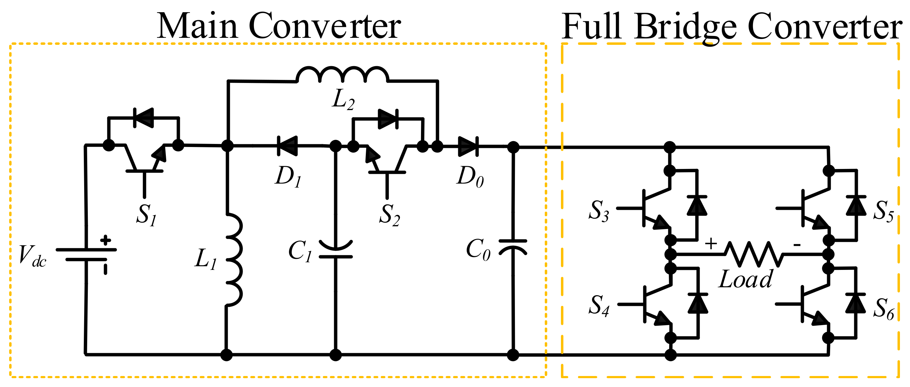
Figure 1.
The proposed single source multilevel inverter.
Figure 1.
The proposed single source multilevel inverter.
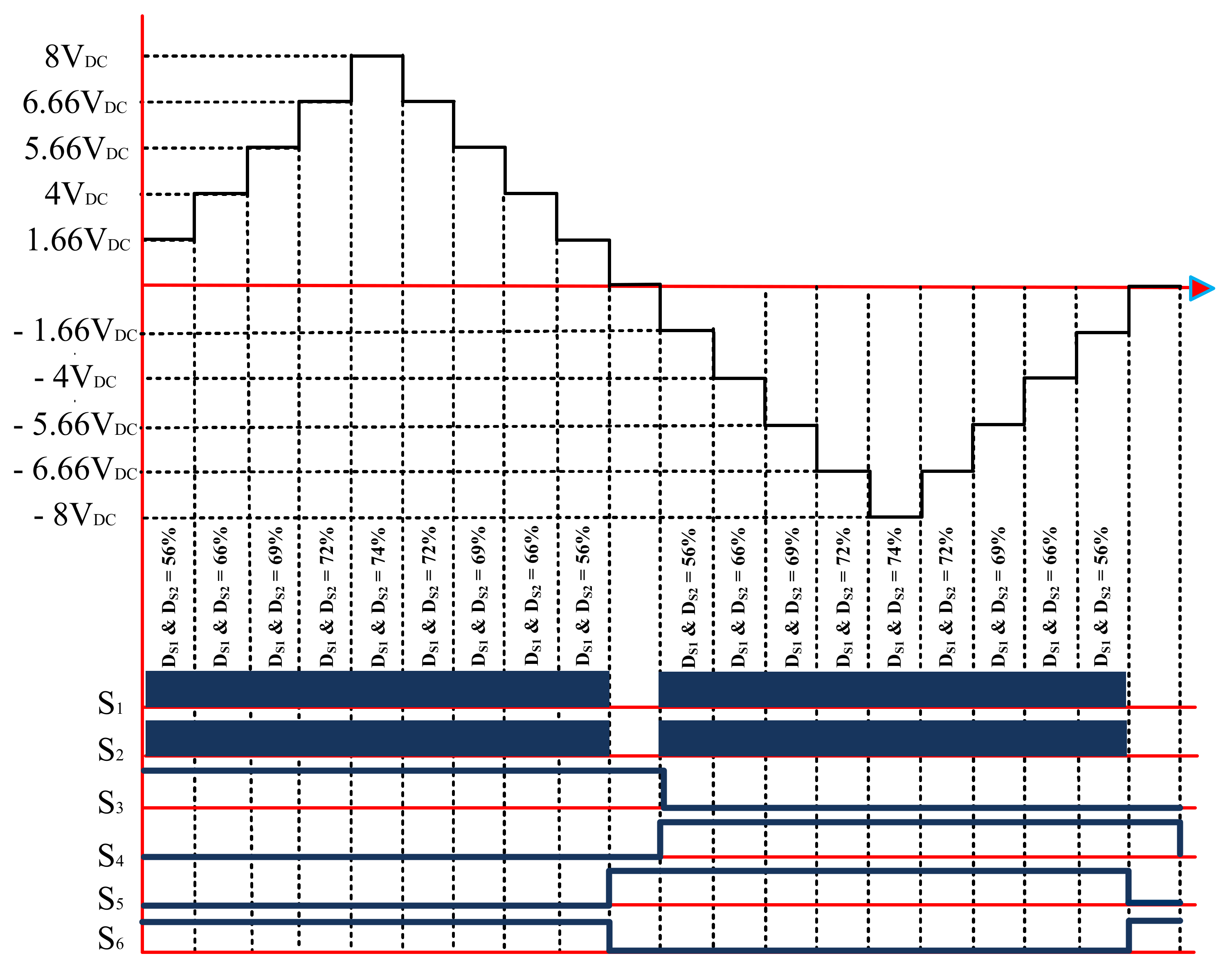
Figure 2.
Switching pattern and duty cycle of switches in one-cycle for the proposed multilevel inverter (ex: the number of levels = 11 and gain = 8).
Figure 2.
Switching pattern and duty cycle of switches in one-cycle for the proposed multilevel inverter (ex: the number of levels = 11 and gain = 8).
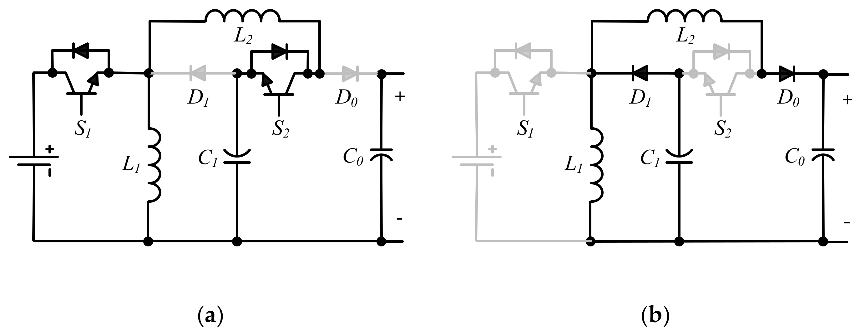
Figure 3.
The mode of the main converter: (a) on mode; (b) off mode.
Figure 3.
The mode of the main converter: (a) on mode; (b) off mode.
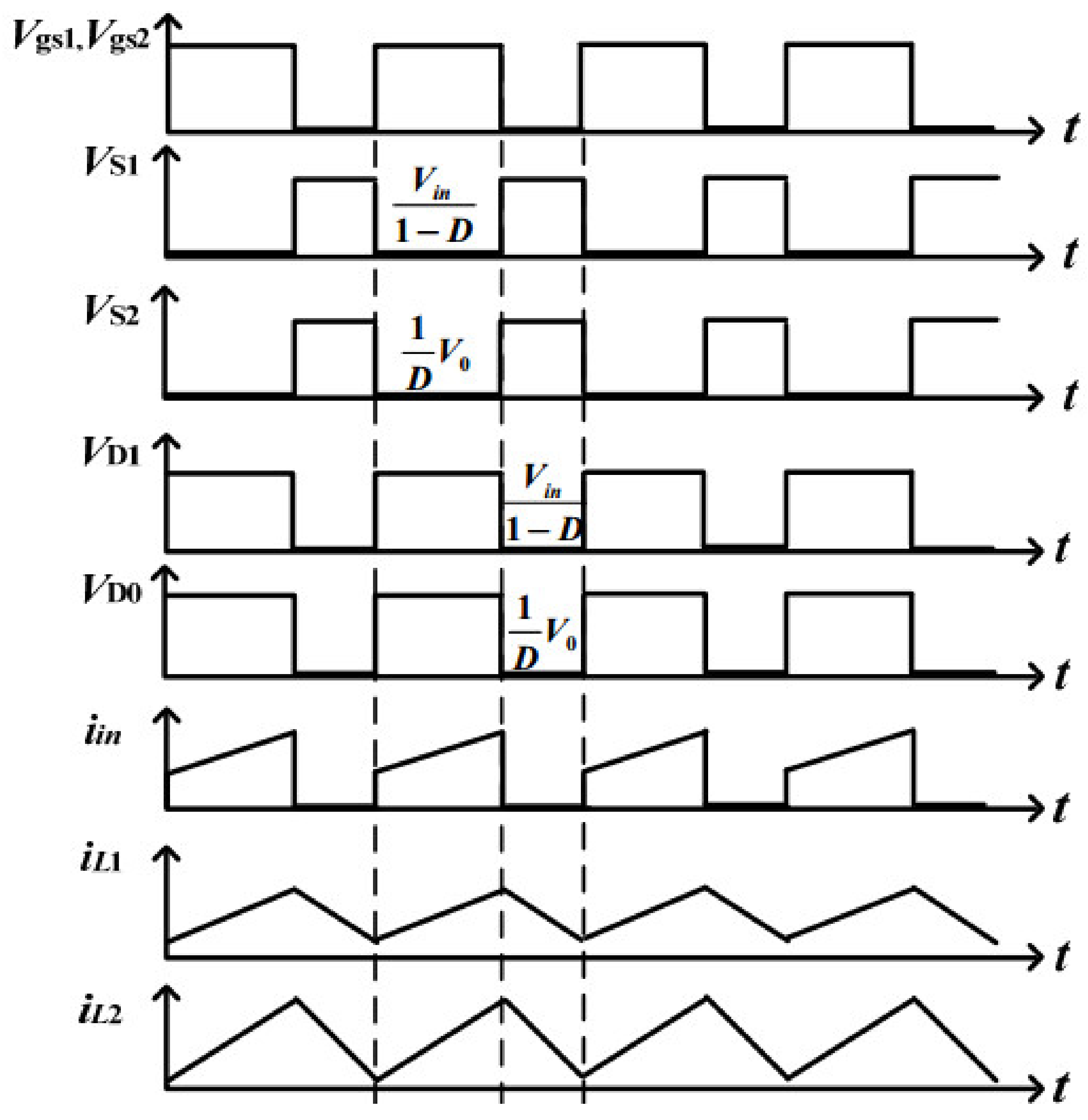
Figure 4.
The behaviors of the components for two modes.
Figure 4.
The behaviors of the components for two modes.
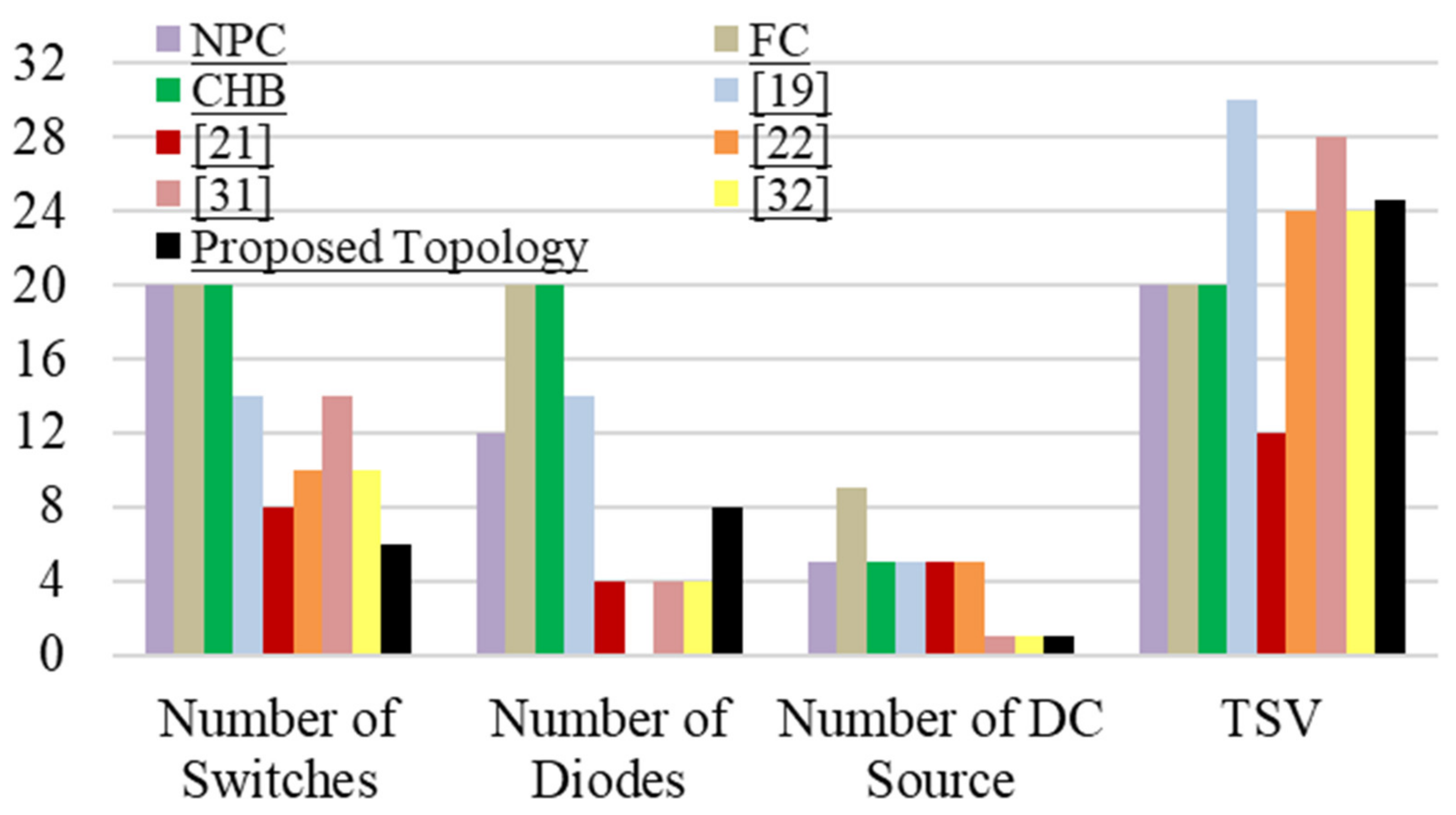
Figure 5.
Comparative studies: The number of switches, number of diodes, number of sources and TSV, in terms of the number of levels.
Figure 5.
Comparative studies: The number of switches, number of diodes, number of sources and TSV, in terms of the number of levels.
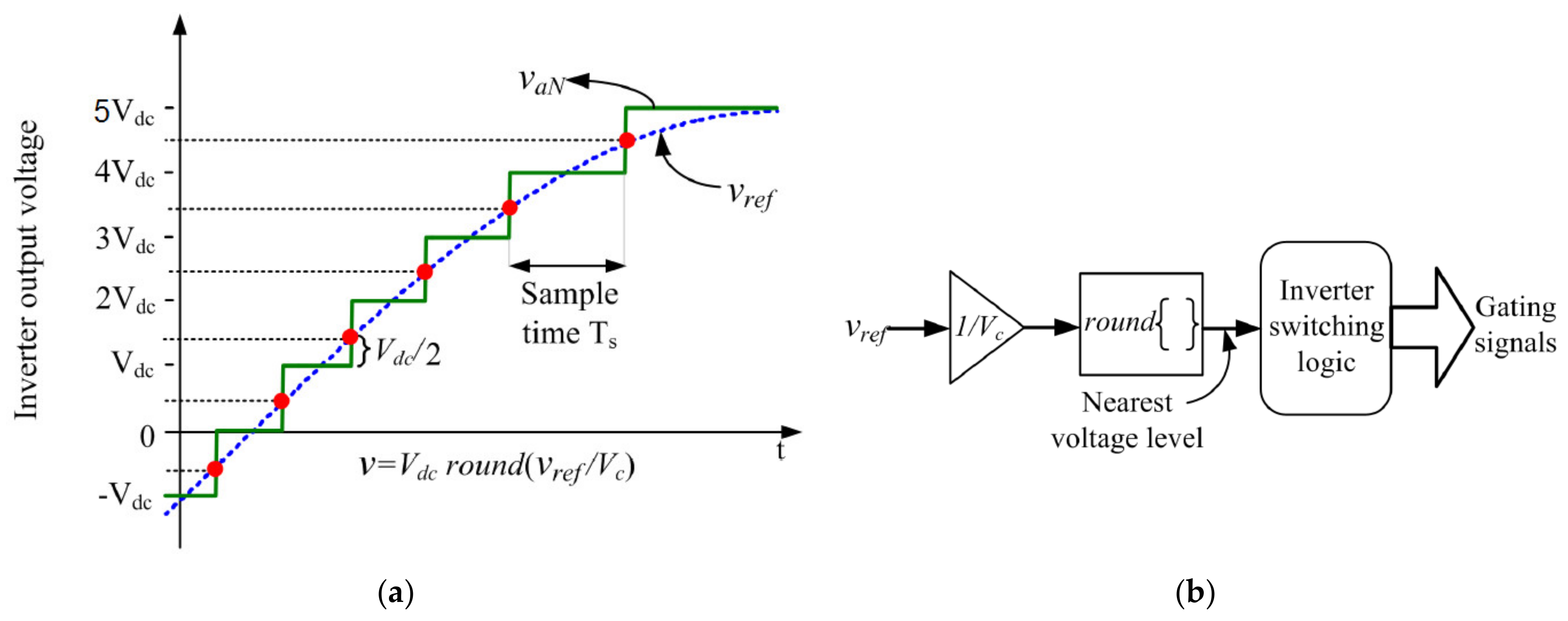
Figure 6.
Nearest level control: (a) Waveform synthesis; (b) Control diagram.
Figure 6.
Nearest level control: (a) Waveform synthesis; (b) Control diagram.
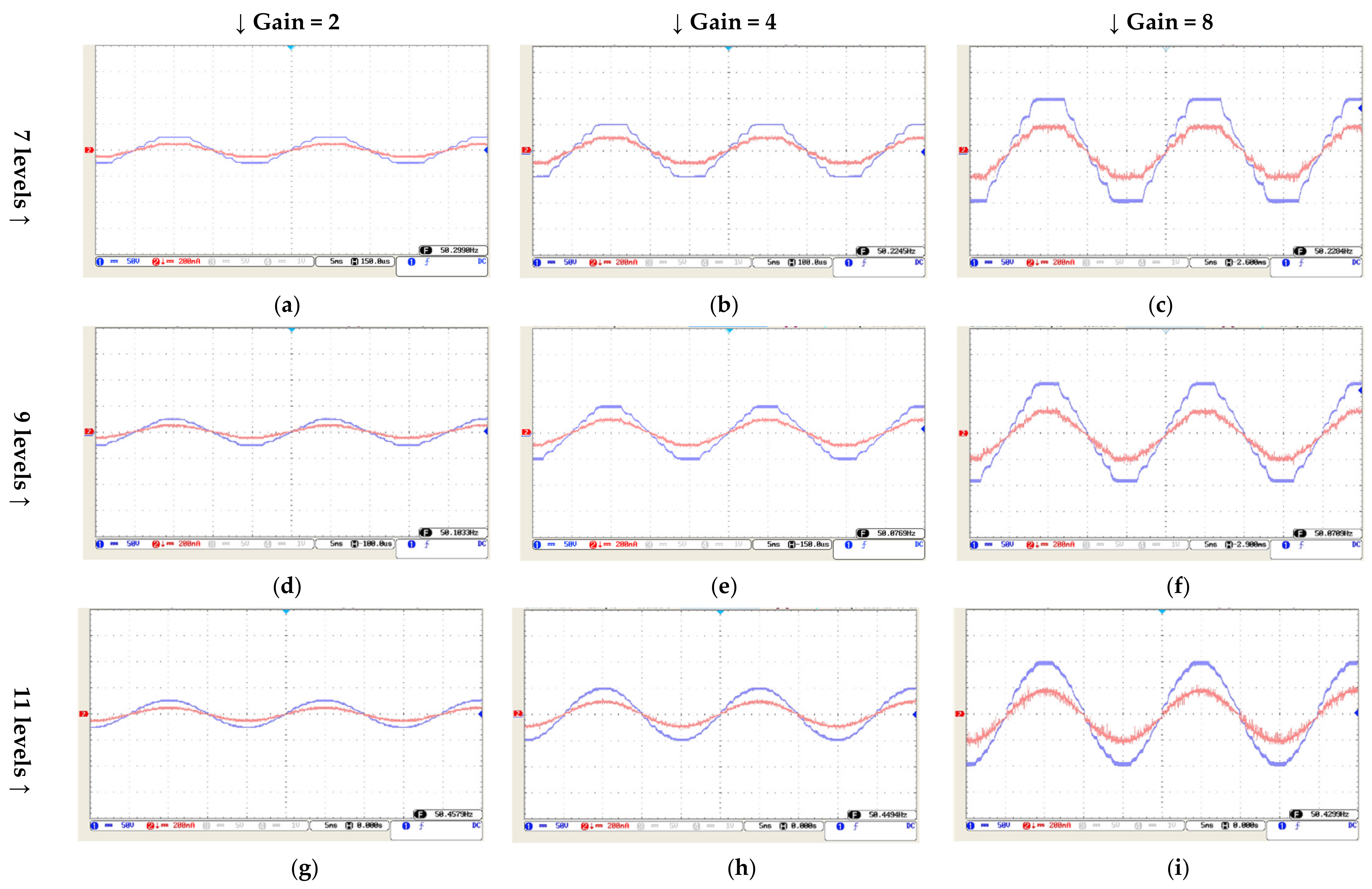
Figure 7.
Simulation waveform of output voltages and currents for the proposed multilevel inverter: (a) levels = 7, gain = 2; (b) levels = 7, gain = 4; (c) levels = 7, gain = 8; (d) levels = 9, gain = 2; (e) levels = 9, gain = 4; (f) levels = 9, gain = 8; (g) levels = 11, gain = 2; (h) levels = 11, gain = 4; (i) levels = 11, gain = 8.
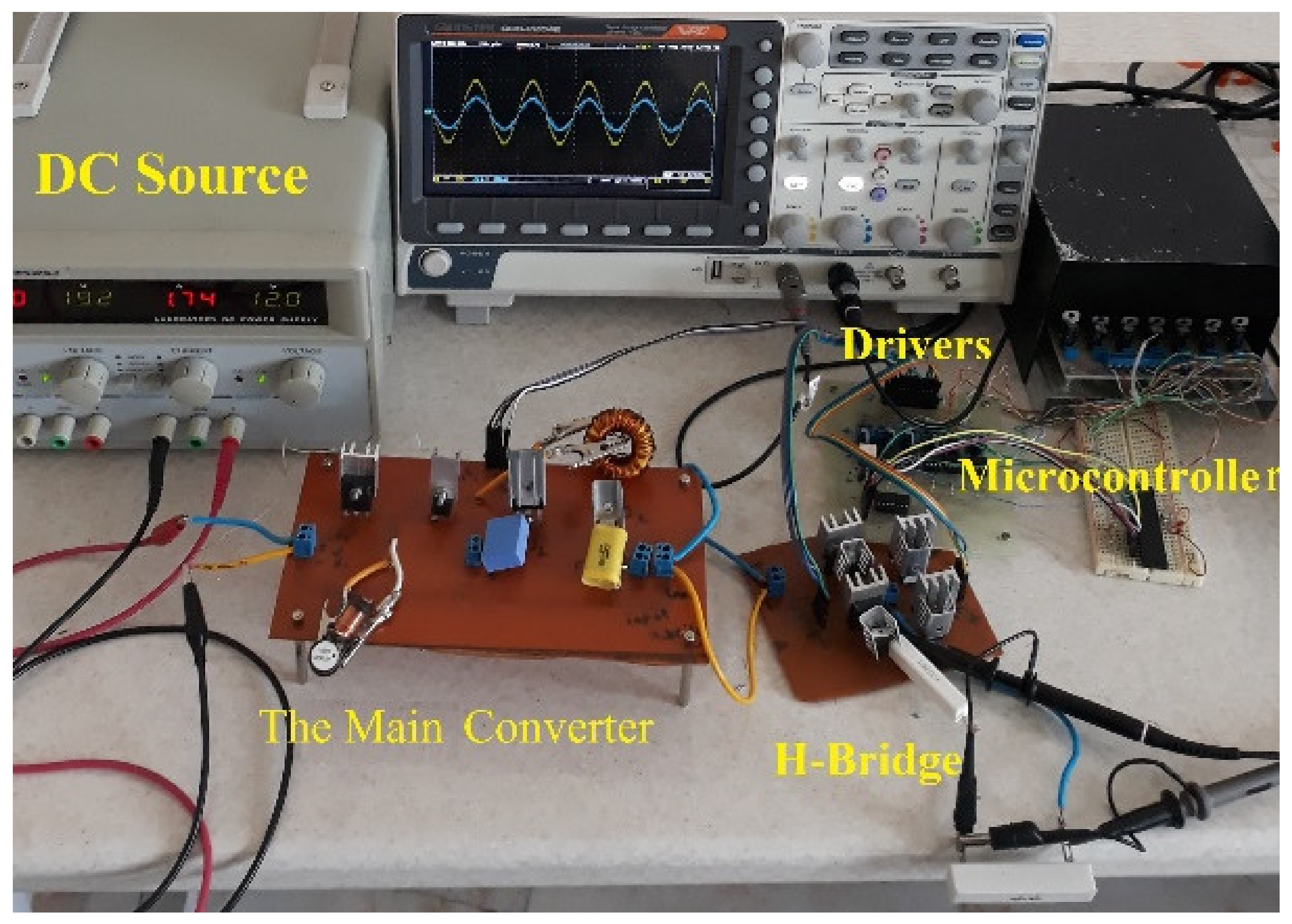
Figure 8.
Experimental setup in the laboratory.
Figure 8.
Experimental setup in the laboratory.
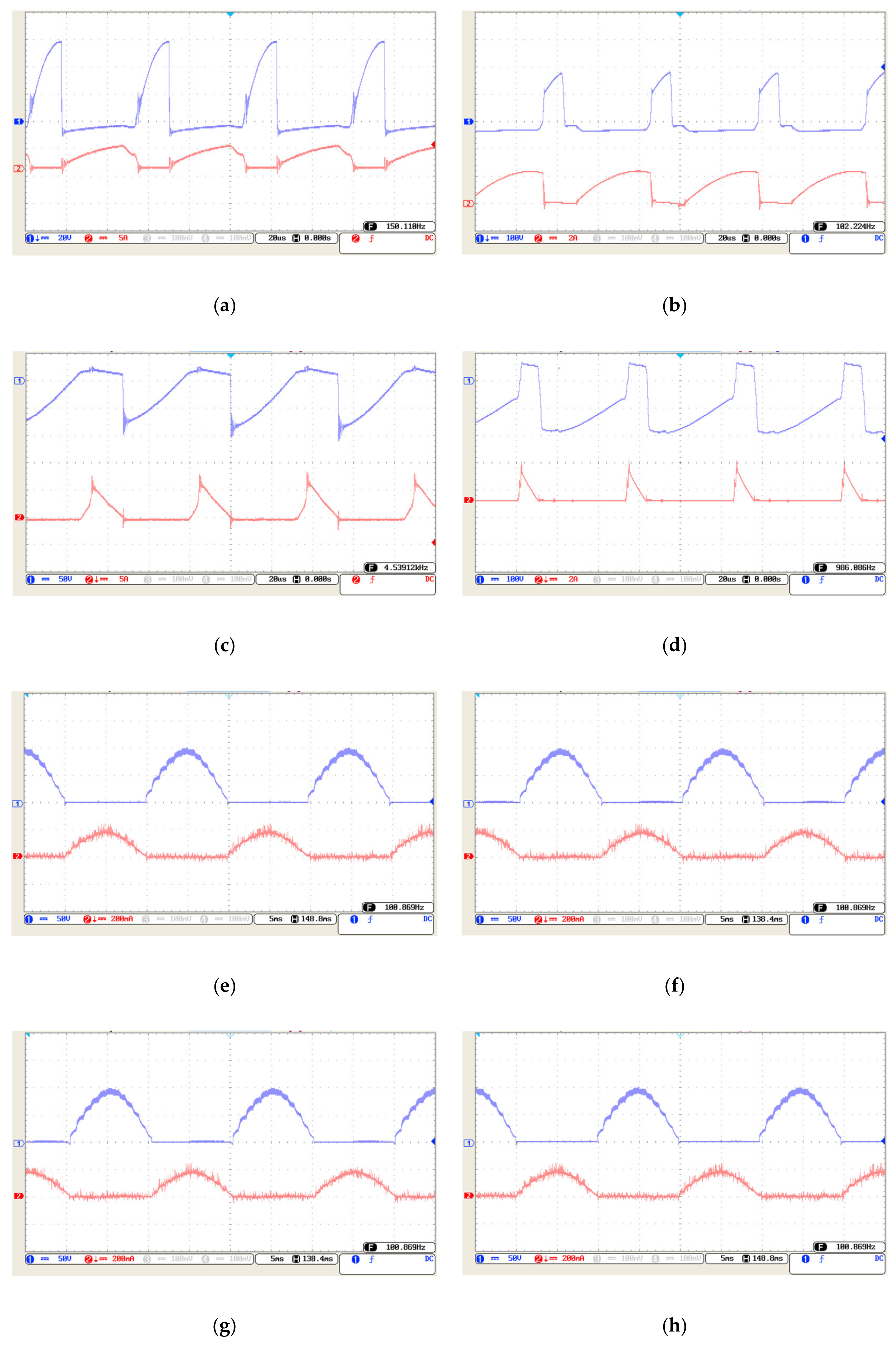
Figure 9.
The experimental test waveform of output voltages and currents for the proposed multilevel inverter: (a) levels = 7, gain = 2; (b) levels = 7, gain = 4; (c) levels = 7, gain = 8; (d) levels = 9, gain = 2; (e) levels = 9, gain = 4; (f) levels = 9, gain = 8; (g) levels = 11, gain = 2; (h) levels = 11, gain = 4; (i) levels = 11, gain = 8.
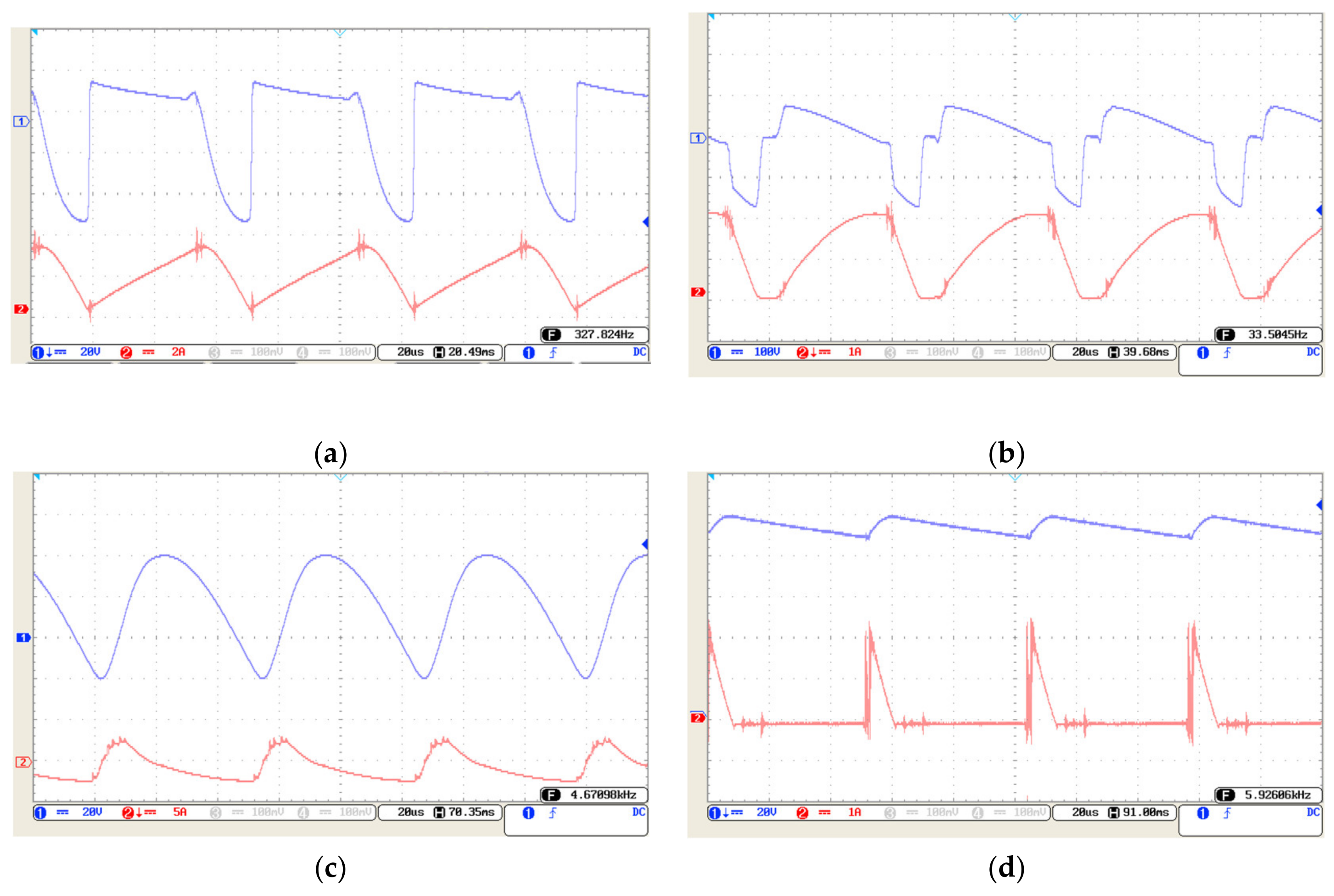
Figure 10.
Experimental test waveform of output voltages and currents for the proposed multilevel inverter: (a) the voltage and current of S1; (b) the voltage and current of S2; (c) the voltage and current of D1; (d) the voltage and current of D0; (e) the voltage and current of S3; (f) the voltage and current of S4; (g) the voltage and current of S5; (h) the voltage and current of S6.
Figure 11.
Experimental test waveform of output voltages and currents for the proposed multilevel inverter: (a) the voltage and current of L1; (b) the voltage and current of L2; (c) the voltage and current of C1; (d) the voltage and current of C0.
Figure 11.
Experimental test waveform of output voltages and currents for the proposed multilevel inverter: (a) the voltage and current of L1; (b) the voltage and current of L2; (c) the voltage and current of C1; (d) the voltage and current of C0.
Table 1.
Switching table level = 11, gain = 8.
Table 1.
Switching table level = 11, gain = 8.
| Voltage Level | Duty Cycle S1 (%) | Duty Cycle S2 (%) | S3 | S4 | S5 | S6 |
|---|
| Positive Level | 8 VDC | 74 | 74 | 1 | 0 | 0 | 1 |
| 6.66 VDC | 72 | 72 | 1 | 0 | 0 | 1 |
| 5.66 VDC | 69 | 69 | 1 | 0 | 0 | 1 |
| 4 VDC | 66 | 66 | 1 | 0 | 0 | 1 |
| 1.66 VDC | 56 | 56 | 1 | 0 | 0 | 1 |
| Zero Level | 0 | 0 | 0 | 1 | 0 | 1 | 0 |
| 0 | 0 | 0 | 0 | 1 | 0 | 1 |
| Negative Level | −1.66 VDC | 56 | 56 | 0 | 1 | 1 | 0 |
| −4 VDC | 66 | 66 | 0 | 1 | 1 | 0 |
| −5.66 VDC | 69 | 69 | 0 | 1 | 1 | 0 |
| −6.66 VDC | 72 | 72 | 0 | 1 | 1 | 0 |
| −8 VDC | 74 | 74 | 0 | 1 | 1 | 0 |
| Num. of turning on per 1-cycle | 20,000 | 20,000 | 1 | 1 | 2 | 2 |
Table 2.
Switching table level = 11, gain = 4.
Table 2.
Switching table level = 11, gain = 4.
| Voltage Level | Duty Cycle S1 (%) | Duty Cycle S2 (%) | S3 | S4 | S5 | S6 |
|---|
| Positive Level | 4 VDC | 66 | 66 | 1 | 0 | 0 | 1 |
| 3.33 VDC | 64 | 64 | 1 | 0 | 0 | 1 |
| 2.83 VDC | 62 | 62 | 1 | 0 | 0 | 1 |
| 2 VDC | 58 | 58 | 1 | 0 | 0 | 1 |
| 0.84 VDC | 47 | 47 | 1 | 0 | 0 | 1 |
| Zero Level | 0 | 0 | 0 | 1 | 0 | 1 | 0 |
| 0 | 0 | 0 | 0 | 1 | 0 | 1 |
| Negative Level | −0.84 VDC | 47 | 47 | 0 | 1 | 1 | 0 |
| −2 VDC | 58 | 58 | 0 | 1 | 1 | 0 |
| −2.83 VDC | 63 | 63 | 0 | 1 | 1 | 0 |
| −3.33 VDC | 72 | 72 | 0 | 1 | 1 | 0 |
| −4 VDC | 66 | 66 | 0 | 1 | 1 | 0 |
| Num. of turning on per 1-cycle | 20,000 | 20,000 | 1 | 1 | 2 | 2 |
Table 3.
Switching table level = 11, gain = 2.
Table 3.
Switching table level = 11, gain = 2.
| Voltage Level | Duty Cycle S1 (%) | Duty Cycle S2 (%) | S3 | S4 | S5 | S6 |
|---|
| Positive Level | 2 VDC | 58 | 58 | 1 | 0 | 0 | 1 |
| 1.66 VDC | 56 | 56 | 1 | 0 | 0 | 1 |
| 1.41 VDC | 54 | 54 | 1 | 0 | 0 | 1 |
| 1 VDC | 50 | 50 | 1 | 0 | 0 | 1 |
| 0.42 VDC | 39 | 39 | 1 | 0 | 0 | 1 |
| Zero Level | 0 | 0 | 0 | 1 | 0 | 1 | 0 |
| 0 | 0 | 0 | 0 | 1 | 0 | 1 |
| Negative Level | −0.42 VDC | 39 | 39 | 0 | 1 | 1 | 0 |
| −1 VDC | 50 | 50 | 0 | 1 | 1 | 0 |
| −1.41 VDC | 54 | 54 | 0 | 1 | 1 | 0 |
| −1.66 VDC | 56 | 56 | 0 | 1 | 1 | 0 |
| −2 VDC | 58 | 58 | 0 | 1 | 1 | 0 |
| Num. of turning on per 1-cycle | 20,000 | 20,000 | 1 | 1 | 2 | 2 |
Table 4.
Switching table level = 9, gain = 8.
Table 4.
Switching table level = 9, gain = 8.
| Voltage Level | Duty Cycle S1 (%) | Duty Cycle S2 (%) | S3 | S4 | S5 | S6 |
|---|
| Positive Level | 8 VDC | 74 | 74 | 1 | 0 | 0 | 1 |
| 5.83 VDC | 70 | 70 | 1 | 0 | 0 | 1 |
| 3.33 VDC | 64 | 64 | 1 | 0 | 0 | 1 |
| 1.66 VDC | 56 | 56 | 1 | 0 | 0 | 1 |
| Zero Level | 0 | 0 | 0 | 1 | 0 | 1 | 0 |
| 0 | 0 | 0 | 0 | 1 | 0 | 1 |
| Negative Level | −1.66 VDC | 56 | 56 | 0 | 1 | 1 | 0 |
| −3.33 VDC | 64 | 64 | 0 | 1 | 1 | 0 |
| −5.83 VDC | 70 | 70 | 0 | 1 | 1 | 0 |
| −8 VDC | 74 | 74 | 0 | 1 | 1 | 0 |
| Num. of turning on per 1-cycle | 20,000 | 20,000 | 1 | 1 | 2 | 2 |
Table 5.
Switching table level = 9, gain = 4.
Table 5.
Switching table level = 9, gain = 4.
| Voltage Level | Duty Cycle S1 (%) | Duty Cycle S2 (%) | S3 | S4 | S5 | S6 |
|---|
| Positive Level | 4 VDC | 66 | 66 | 1 | 0 | 0 | 1 |
| 2.91 VDC | 63 | 63 | 1 | 0 | 0 | 1 |
| 1.66 VDC | 56 | 56 | 1 | 0 | 0 | 1 |
| 0.84 VDC | 47 | 47 | 1 | 0 | 0 | 1 |
| Zero Level | 0 | 0 | 0 | 1 | 0 | 1 | 0 |
| 0 | 0 | 0 | 0 | 1 | 0 | 1 |
| Negative Level | −0.84 VDC | 47 | 47 | 0 | 1 | 1 | 0 |
| −1.66 VDC | 56 | 56 | 0 | 1 | 1 | 0 |
| −2.91 VDC | 63 | 63 | 0 | 1 | 1 | 0 |
| −4 VDC | 66 | 66 | 0 | 1 | 1 | 0 |
| Num. of turning on per 1-cycle | 20,000 | 20,000 | 1 | 1 | 2 | 2 |
Table 6.
Switching table level = 9, gain = 2.
Table 6.
Switching table level = 9, gain = 2.
| Voltage Level | Duty Cycle S1 (%) | Duty Cycle S2 (%) | S3 | S4 | S5 | S6 |
|---|
| Positive Level | 2 VDC | 58 | 58 | 1 | 0 | 0 | 1 |
| 1.45 VDC | 55 | 55 | 1 | 0 | 0 | 1 |
| 0.84 VDC | 47 | 47 | 1 | 0 | 0 | 1 |
| 0.42 VDC | 39 | 39 | 1 | 0 | 0 | 1 |
| Zero Level | 0 | 0 | 0 | 1 | 0 | 1 | 0 |
| 0 | 0 | 0 | 0 | 1 | 0 | 1 |
| Negative Level | −0.42 VDC | 39 | 39 | 0 | 1 | 1 | 0 |
| −0.84 VDC | 47 | 47 | 0 | 1 | 1 | 0 |
| −1.45 VDC | 55 | 55 | 0 | 1 | 1 | 0 |
| −2 VDC | 58 | 58 | 0 | 1 | 1 | 0 |
| Num. of turning on per 1-cycle | 20,000 | 20,000 | 1 | 1 | 2 | 2 |
Table 7.
Switching table level = 7, gain = 8.
Table 7.
Switching table level = 7, gain = 8.
| Voltage Level | Duty Cycle S1 (%) | Duty Cycle S2 (%) | S3 | S4 | S5 | S6 |
|---|
| Positive Level | 8 VDC | 74 | 74 | 1 | 0 | 0 | 1 |
| 5.41 VDC | 69 | 69 | 1 | 0 | 0 | 1 |
| 2.5 VDC | 61 | 61 | 1 | 0 | 0 | 1 |
| Zero Level | 0 | 0 | 0 | 1 | 0 | 1 | 0 |
| 0 | 0 | 0 | 0 | 1 | 0 | 1 |
| Negative Level | −2.5 VDC | 61 | 61 | 0 | 1 | 1 | 0 |
| −5.41 VDC | 69 | 69 | 0 | 1 | 1 | 0 |
| −8 VDC | 74 | 74 | 0 | 1 | 1 | 0 |
| Num. of turning on per 1-cycle | 20,000 | 20,000 | 1 | 1 | 2 | 2 |
Table 8.
Switching table level = 7, gain = 4.
Table 8.
Switching table level = 7, gain = 4.
| Voltage Level | Duty Cycle S1 (%) | Duty Cycle S2 (%) | S3 | S4 | S5 | S6 |
|---|
| Positive Level | 4 VDC | 66 | 66 | 1 | 0 | 0 | 1 |
| 2.70 VDC | 62 | 62 | 1 | 0 | 0 | 1 |
| 1.25 VDC | 52 | 52 | 1 | 0 | 0 | 1 |
| Zero Level | 0 | 0 | 0 | 1 | 0 | 1 | 0 |
| 0 | 0 | 0 | 0 | 1 | 0 | 1 |
| Negative Level | −1.25 VDC | 52 | 52 | 0 | 1 | 1 | 0 |
| −2.70 VDC | 62 | 62 | 0 | 1 | 1 | 0 |
| −4 VDC | 66 | 66 | 0 | 1 | 1 | 0 |
| Num. of turning on per 1-cycle | 20,000 | 20,000 | 1 | 1 | 2 | 2 |
Table 9.
Switching table level = 7, gain = 2.
Table 9.
Switching table level = 7, gain = 2.
| Voltage Level | Duty Cycle S1 (%) | Duty Cycle S2 (%) | S3 | S4 | S5 | S6 |
|---|
| Positive Level | 2 VDC | 58 | 58 | 1 | 0 | 0 | 1 |
| 1.35 VDC | 53 | 53 | 1 | 0 | 0 | 1 |
| 0.62 VDC | 44 | 44 | 1 | 0 | 0 | 1 |
| Zero Level | 0 | 0 | 0 | 1 | 0 | 1 | 0 |
| 0 | 0 | 0 | 0 | 1 | 0 | 1 |
| Negative Level | −0.62 VDC | 44 | 44 | 0 | 1 | 1 | 0 |
| −1.35 VDC | 53 | 53 | 0 | 1 | 1 | 0 |
| −2 VDC | 58 | 58 | 0 | 1 | 1 | 0 |
| Num. of turning on per 1-cycle | 20,000 | 20,000 | 1 | 1 | 2 | 2 |
Table 10.
Simulation configuration.
Table 10.
Simulation configuration.
| Switches | IGBT |
| Diodes | Diode |
| Inductors | L1 = 50 μH | L2 = 250 μH |
| Capacitors | C0 = 2 μF | C1 = 1 μF |
| DC Source | 36 V |
| Load | 500 Ω |
Table 11.
Specifications of the prototype setup configuration.
Table 11.
Specifications of the prototype setup configuration.
| Switches | IGBT FGH60N60SFD (S1,S2)
(S3,S4,S5,S6) IGBT IKW40N120H3 |
| Diodes | RHRP15120 |
| Inductors | L1 = 50 μH | L2 = 250 μH |
| Capacitors | C0 = 2 μF | C1 = 1 μF |
| DC Source | 12 V |
| Optocoupler | HCPL3120 |
| Microcontroller | ATmega32A |
| Buffer | 7404 |
| Load | 500 Ω |
Table 12.
THD% of voltages for nine outputs.
Table 12.
THD% of voltages for nine outputs.
| 7Levels, Gain 2 | 6.61 |
| 7Levels, Gain 4 | 6.70 |
| 7Levels, Gain 8 | 6.82 |
| 9Levels, Gain 2 | 4.88 |
| 9Levels, Gain 4 | 4.77 |
| 9Levels, Gain 8 | 5.27 |
| 11Levels, Gain 2 | 2.08 |
| 11Levels, Gain 4 | 2.28 |
| 11Levels, Gain 8 | 2.29 |


