Article

A Novel Power Decoupling Control Method to Eliminate the Double Line Frequency Ripple of Two Stage Single-Phase DC-AC Power Conversion Systems

Department of Electrical Engineering, Soongsil University, Seoul 06978, Korea
*
Author to whom correspondence should be addressed.
Electronics 2020, 9(6), 931; https://doi.org/10.3390/electronics9060931
Submission received: 18 May 2020 / Revised: 27 May 2020 / Accepted: 29 May 2020 / Published: 3 June 2020
(This article belongs to the Special Issue High Power Electric Traction Systems)

Abstract

:
In two-stage single-phase inverters, inherent double line frequency ripple is present at both the input and output of the front-end converter. Generally, large electrolytic capacitors are used to eliminate this double line frequency ripple. It is well known that low frequency ripple shortens the lifespan of capacitors. Hence, the system reliability can get worse. In order to eliminate the double line frequency ripple, additional hardware combined with an energy storage device is required in most of the methods developed so far. In this paper, a novel power-decoupling control method is proposed to eliminate the double line frequency ripple at the front-end converter of two-stage single phase DC/AC power conversion systems. The proposed control algorithm is composed of two loops, a ripple compensation loop and an average voltage control loop, and no extra hardware is required. Since the proposed method does not require information from the phase-locked-loop (PLL) of the inverter, it is independent of inverter control. In order to verify the validity and feasibility of the proposed algorithm a 5 kW Dual Active Bridge (DAB) DC/DC converter and a single-phase inverter are implemented. The effectiveness of the proposed method is verified through the simulation and experimental results.

1. Introduction

Two-stage DC/AC power conversion systems are widely used since they provide galvanic isolation between the input and output, and a flexible voltage gain for the rear-end inverter. By boosting the low voltage of the source to a suitable DC voltage level, front-end converters play an important role in providing a suitable input DC voltage for the rear-end Voltage Source Inverters (VSIs) to produce an AC voltage [1].
For two-stage single-phase DC/AC systems, the Dual Active Bridge (DAB) converter has attracted a lot of research interests as a front-end converter due to its high-power density, galvanic isolation, and bidirectional power flow. The DAB converter is an efficient topology for bidirectional power applications due to its inherent soft switching capability i.e., ZVS. [2,3].
Typically, a two-stage single phase DC-AC converter system is comprised of a first stage DC-DC converter with galvanic isolation and a second stage single-phase DC-AC inverter [4]. It is well known that the instantaneous input power of the two-stage single-phase inverter pulsates at the double line frequency, which results in double line frequency ripples at both ends of the front-end dc-dc converter. Therefore, large electrolytic capacitors are used at the input to eliminate the double line frequency ripple [5] and to maintain a constant DC link voltage by balancing the power mismatch between the front-end and rear-end converters. Although electrolytic capacitors have higher capacitance to volume ratio than those of other types, their life spans are shorter than those of the other components used in converters. Therefore, the reliability of a system depends heavily on it. It is well known that the electrolytic capacitor is about thirty times less reliable than film capacitors with the help under similar conditions [6,7]. Since low frequency ripple current accelerates the aging of a capacitor, it should be reduced by control algorithms such as Power Decoupling Techniques (PDTs). The main idea of PDTs is to inject the ripple power to an energy storage device such as a capacitor with the help of additional circuits [8] as shown in Figure 1. However, this cannot be achieved without an increase in the volume, weight and cost of the system.
In order to diminish low frequency ripple current and avoid using massive electrolytic capacitors, a method with a DC active filter has been proposed in [9]. In this method, elimination of input ripple current is achieved by using a dc chopper to inject ripple current. A drawback of this approach is that it requires an auxiliary DC chopper, which results in a massive volume and a higher cost of the system [10]. Another ripple current reduction method using a current-loop control for three-phase DC-DC converters can be found in [11]. However, it requires a large capacitor as an energy buffer at the output of the converter since the ripple at the output is not controlled.
Another method proposed in [12] shows that a DC active filter can be implemented with no extra switching devices. The decoupling capacitor is connected at the center tap of the isolation transformer, and common mode voltage is used to decouple the pulsating power. However, the current rating of the transformer is significantly increased, which increases the losses. A ripple rejection technique utilizing current control was proposed in [13]. However, it is not possible to reduce the DC-link capacitors. Moreover, since it uses an electrolytic capacitor for the DC-link, the reliability of system is not sufficiently increased. Three port power decoupling systems were proposed in [14,15,16]. However, these methods require a three-winding transformer with additional circuits. In addition, the control is complex. Hence, the cost, weight, size and complexity of the systems are increased.
A DAB converter is often employed as a front-end DC-DC converter of two stage DC/AC power conversion systems. There are two categories of DAB converters: one is the current-fed DAB and the other is the voltage-fed DAB. In the current-fed DAB, an inductor is required at the input of the DAB to control the current, which increases the volume and cost of the converter. In terms of the component count, the voltage-fed DAB converter is better than the current-fed DAB converter because it does not require a large inductor. However, it is a challenge to use a voltage fed DAB for the power decoupling control since current control is essential in the conventional methods in [17,18,19]. Therefore, most double line frequency component elimination methods have been developed based on the current-fed topology and ripple current control. In this paper, a novel voltage control based double line frequency ripple elimination method is proposed for two stage DC/AC power converters as shown in Figure 2. The double line frequency ripple is extracted by the Band Pass Filter (BPF) and it is compensated by the PI controller. The output of the DC/DC converter is also regulated by the PI controller. However, it is loosely controlled to allow the double line frequency ripple (i.e., the 120 Hz component in this case) to oscillate around the desired output voltage. Since the proposed method does not require phase information of the double line frequency ripple, there is no need to obtain it from the Phase Locked Loop (PLL) of the inverter. Therefore, the double line frequency ripple elimination can be performed without depending on the inverter control. The capacitance values of the input decoupling capacitor and the output DC link capacitor can be significantly reduced by the proposed method.
This paper is organized as follows. In Section 2, an overview of the principle of double line frequency generation and a summary of the proposed control method to eliminate the double line frequency ripple are presented. In Section 3, a simplified model of a DAB is presented to obtain the control-to-output and control-to-input transfer functions for the design of the ripple elimination control loop and the average DC-link voltage control. In Section 4, the design of the proposed control method for double line frequency ripple elimination is discussed in detail. In Section 5, simulation and experimental results are presented along with a comparison between the proposed and conventional ripple elimination methods in terms of reductions in the capacitance, capacitor volume and double line frequency ripple. Finally, some conclusions are given in Section 6.

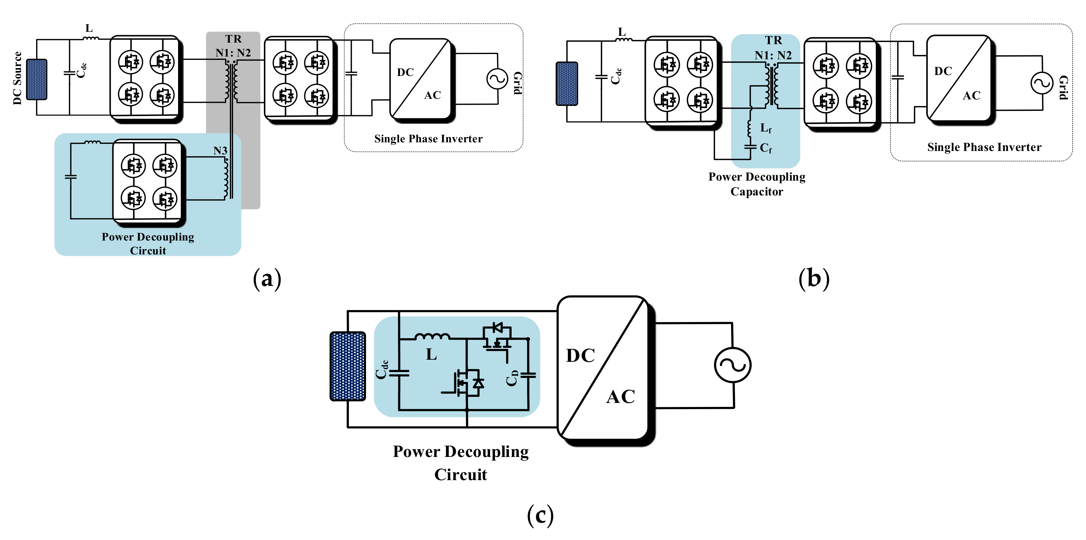
2. Double Line Frequency Ripple

As mentioned earlier, a typical two-stage single phase DC-AC power conversion system is composed of a DC-DC converter and a single-phase VSI. The input current and the voltage of the VSI are DCs. However, they contain high frequency switching noises and a fundamental low frequency component. The instantaneous output power of the two-stage single-phase inverter pulsates at twice the frequency of the output voltage, which results in a second harmonic current at the input of the single-phase inverter. This harmonic current propagates back into the front-end dc–dc converter and the input source. Therefore, it causes higher current stresses for the power switches and produces additional power losses. It is well known that it may shorten the life of input dc voltage sources such as batteries or fuel cells and degrade the power conversion efficiency.
The principle for the second harmonic generated by the single-phase inverter can be derived as follows. In a single-phase VSI system, the current injected into the AC grid I(t) and the grid AC voltage U(t) can be represented by Equations (1) and (2), respectively.
U ( t ) = U m s i n ω o t
I ( t ) = I m s i n ω o t + ϕ
where, ωo represents the AC line frequency, and Um and Im are the amplitude of the output voltage and current, respectively. ϕ is the phase between the current and the voltage. The instantaneous input power Pt can be calculated by Equation (3).
P t = 1 2 U m I m + 1 2 U m I m cos ( 2 ω o t + ϕ )
It can be easily found from Equation (3) that the instantaneous power at the input is composed of two terms, an average DC power and a pulsating power that oscillates at twice the line frequency. A straightforward way to mitigate the ripple power at the DC source side is to use a bulky capacitor. The capacitors can be placed with the inverter stage or connected in parallel with the DC source. However, since the required capacitance is relatively large, many bulky electrolytic capacitors should be connected in parallel. The sizing of the required capacitance value to suppress the double line frequency ripple can be performed as follows. During a half-line cycle, the energy being charged to or discharged from the decoupling capacitor can be calculated by Equation (4).
E C D = 1 2 U 2 DC _ max U 2 DC _ min
where UDC_max and UDC_min are the maximum and minimum voltages across the decoupling capacitor, respectively. Therefore, the required decoupling capacitance can be calculated as Equation (5) [20].
C D = P d c 2 π f g r i d U d c Δ u
where fgrid is the line frequency, Udc is the average DC voltage across the decoupling capacitor CD, and Δu is the allowable ripple voltage across CD. It is suggested from Equation (5) that the decoupling capacitor should be placed at the high voltage side rather than placing it at the low voltage side so the size of the capacitor can be reduced [21]. In order to avoid using a bulky decoupling capacitor to suppress the double line frequency ripple, power decoupling-based control is preferred to buffer the ripple power in two-stage inverters. Since the amplitude of the double line frequency ripple current is determined by the output impedance of the front-end dc–dc converter and the impedance of the dc-bus capacitor at double line frequency, it can be reduced by increasing its output impedance at double line frequency with suitable control schemes.
In this paper, a novel voltage control based double line frequency ripple elimination method is proposed for two stage DC/AC power conversion systems as shown in Figure 2. The double line frequency ripple is extracted by the BPF and it is compensated by the PI controller. The output of the DC/DC converter is also regulated by the PI controller. However, it is loosely controlled to allow the double line frequency ripple (i.e., the 120 Hz component in this case) to oscillate around the desired value of the output. Thanks to the ripple reduction capability of the proposed method, a decoupling capacitor with an even lower capacitance value can be employed at both ends of the front-end DC-DC converter.

3. Simplified Modeling of DAB for Double Line Frequency Ripple Elimination

In this section, simplified modeling of the DAB for power decoupling control is introduced for the control of a converter as well as the elimination of double line frequency ripple. The DAB is a bidirectional DC-DC converter consisting of eight active switches, a high frequency transformer, a leakage inductor and DC-link capacitors as illustrated in Figure 2. Where VDC and VDC_Link are the input DC source voltage and DC-link voltage of the VSI, respectively. Llk is the leakage inductance of the transformer, and S1–8 are the power semiconductor switches in the DAB converter.
As shown in Figure 3, S1,4 and S2,3 are the control gate signals for the primary switch Spri, and S5,8 and S6,7 are the control gate signals for the secondary bridge Ssec. Here, power is delivered from the low voltage side bridge to the high voltage side bridge. When the phase shift δ of the secondary bridge signal is positive +δ, the power is delivered from the primary bridge to the secondary bridge. When it is negative −δ, the power flow is reversed. Figure 3 also shows the Transformer leakage current and voltage waveforms at a given phase shift. By using Kirchhoff’s voltage equation, the slope of the inductor current can be represented by Equation (6).
d i l k d t = V p r i ( t ) V sec ( t ) L k
A half switching cycle can be divided into two intervals, 0 < θ < δ and δ < θ < π. By solving the above equation for each interval, Equations (7) and (8) can be obtained.
V DC + V DC _ link n = L k ( I 1 + I 2 ) d T f o r 0 < t < d T
V DC V DC _ link n = L k ( I 1 + I 2 ) ( 1 d ) T f o r d T < t < T
where ‘n’ is the turns-ratio of the transformer, T is a half-cycle of a period, I1 and I2 are the inductor currents, and δ/π is the duty d obtained by the phase shift between two bridges.
By averaging Equations (7) and (8), as shown in [22], the average output current of the converter can be represented by Equation (9).
I P 2 = 1 d d T V DC n L k
The output power of the DAB converter can be derived using the average current in Equation (9), as shown in Equation (10).
P = V DC _ link I P 2 = 1 d d T V DC V DC _ link n L k
Equation (10) explains the relationship between the power transferred to the output as a function of the duty cycle. Where d denotes the phase shift (δ/π). The maximum power flow occurs at d = ±0.5, as shown in Figure 4. Although the converter can operate with |d| > 0.5 (the dotted lines in Figure 4), the phase shift is usually bounded when |d| ≤ 0.5 to avoid excessive reactive power. The leakage inductance value for the optimal power transfer can be calculated by Equation (11).
L k = ( 1 d ) d V DC V DC _ link n P max
For high-performance control of the converter, to eliminate the low frequency component, a small signal model of the converter needs to be derived first. In order to obtain a small signal average model of the DAB converter, an equivalent circuit of the converter needs to be derived, as shown in Figure 5. Since the DAB converter can be modeled as a controlled DC current source, its equivalent circuit model can be represented by a controlled DC current source and a capacitor connected in parallel with the load.
By using Equation (9), the output current of the DAB converter IP2 can be expressed by Equation (12).
I P 2 = P V DC _ link = V DC n ω L k δ ( 1 | δ | π )
where the negative sign represents the direction of the current. Since the current source is nonlinear, it should be linearized at the operating point δo (at light load), as shown in Equation (13).
G o = d I P 2 d δ = V DC n ω L k ( 1 2 | δ | π )
where Go is the linearized equation of the DAB, which represents the gain of the DAB converter. In addition, ω is equal to 2πfs, and fs is the switching frequency. The linearized small signal model equation for the DAB converter can be obtained as shown in Equation (14).
I P 2 = G o × δ = V DC n ω L k ( 1 2 | δ | π ) δ
The small signal model equation in Equation (14) is a proportional function. A higher gain of the converter can be achieved with a smaller phase shift, and a larger phase shift results in a smaller gain of the converter.
H ( s ) = R L 1 + C DC _ Link R L s
The H(s) in Equation (15) is the transfer function of the output capacitor and the load, as shown in Figure 5. Here, RL is the equivalent load resistance, and CDC_link is the output capacitance. The transfer function of the PI compensator can be expressed by Equation (16).
G c ( s ) = K p 1 + τ s τ s
where Kp is the proportional gain, and τ is the time constant. In a small signal model of a DAB converter, the leakage inductance Lk and the ESR of the capacitor can be neglected for simplicity of analysis, otherwise, the order of the system is increased [23]. Since the leakage inductance is very small and the pole frequency associated with it is far beyond the bandwidth of the controller, it can be neglected. Therefore, the above-mentioned small signal model is valid around the operating frequency.
By using Equations (13) and (15), the control to output transfer functions at each direction of the DAB converter can be derived by Equations (17) and (18), respectively.
G V DC _ link = v DC _ link δ = G o × H ( s ) G V DC _ link = V DC n ω L k 1 2 | δ | π R L 1 + C DC _ Link R L s
Similarly, the control to input voltage transfer function can be obtained by Equation (18).
G V DC = v DC δ = G o × H ( s ) G V DC = V DC _ link n ω L k   1 2 | δ | π R L 1 + C DC R L s
with a pure resistive load, the transfer function is comprised of two poles and one zero. Since the pole frequency is affected by the load resistance, it is low at light loads and high at heavy loads. The order of the transfer function of the DAB converter is the first order at a given operating condition with δo. Therefore, it is easy to design the PI controller for the DAB converter and it can be regarded as another advantage of the proposed method.
In order to verify the validity of the proposed transfer function of the DAB, both MATLAB and PSIM simulations are performed with the specification of the DAB given in Table 1 and Table 2. First, the circuit is implemented in PSIM using the parameters in Table 1 and Table 3, and its transfer function is drawn by using a built-in AC SWEEP function in PSIM. Second, a bode plot of the proposed simplified transfer function of the DAB converter is drawn using MATLAB. As clearly indicated in Figure 6, the Bode plots drawn by MATLAB and PSIM are well matched, which verifies that the proposed simplified model is valid. Therefore, the derived transfer functions can be used to analyze the converter response and to design the closed loop control of the system.

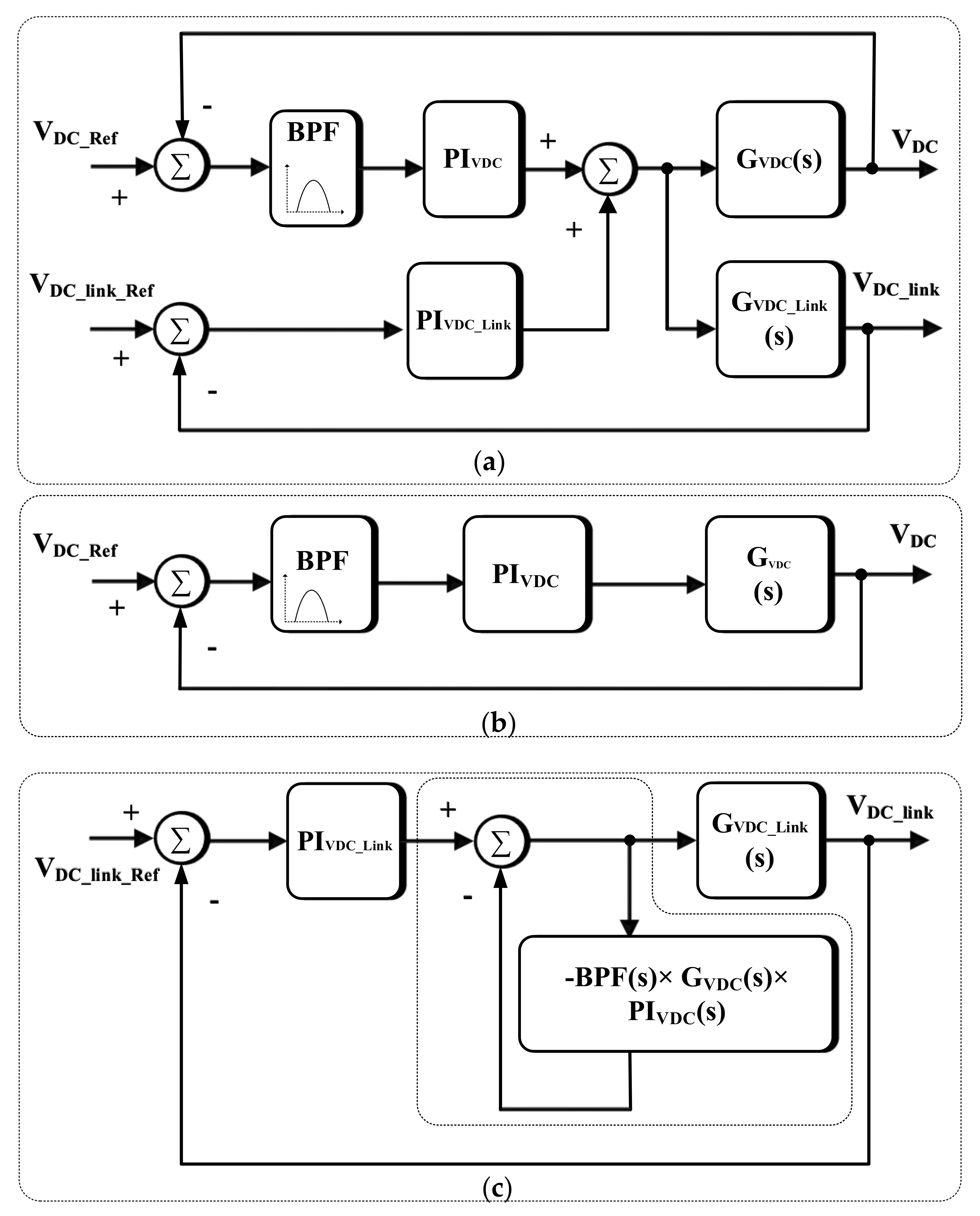
4. Design of the Controllers for DAB Converters Voltage Control and the Elimination of Double Line Frequency Ripple

Figure 7 represents a block diagram of the control loop for a conventional DAB to control the output voltage. Here, the block H(s) represents the transfer function of the output filter and the load of the equivalent circuit model expressed in Equation (15) and Go is the gain of the DAB converter shown in Equation (13). The block with a gain of “−1” indicates the direction of the current IP2 in Figure 7, and Gc(s) represents the transfer function of the PI controller.
There are two controllers in the proposed double line frequency ripple elimination method. One is a PI controller to compensate the double line frequency ripple, and the other is another PI controller to regulate the DC link voltage. As explained earlier, the transfer functions of the DAB converter in each direction are given by Equations (17) and (18).
A block diagram of the proposed control loop is shown in Figure 8a. Figure 8b shows the double line frequency ripple compensation loop, in which the average control loop for the DC link voltage of the VSI is neglected since the ripple compensation loop is much faster than the average control loop. In the ripple compensation loop, where the BPF(s) and PIVDC(s) are the band pass filter and the PI controller, where the transfer functions are expressed in Equations (16) and (19), respectively. Another PI controller, shown as PIVDC_link(s), is used for regulating the average voltage across the DC link capacitor.
At first, the double line frequency ripple compensation loop is designed as shown in Figure 8b. In designing the BPF its center frequency is selected at 120 Hz and the lower value of the damping factor is selected to obtain a higher gain at 120 Hz. Therefore, the transfer function of the BPF can be obtained by Equation (19).
B P F ( s ) = k ω S S 2 + k ω S + ω 2
where, ω is the resonant angular frequency, and k is the damping factor.
The PI controller needs to be designed to reject all of the frequency components other than 120 Hz ripple by allowing a higher gain at 120 Hz. Thus, the loop gain TVDC for the double line frequency ripple compensation loop can be represented by Equation (20).
T ( VDC ) = B P F ( s ) × P I VDC × G VDC
where GVDC is the control to input transfer function in Equation (18).
The double line frequency ripple controllers are designed using MATLAB and the resulting Bode plots are drawn as shown in Figure 9a. The parameters for the PI controller are Kp = −0.3 and the time constant τ = 10 × 10−3. It can be clearly seen from the Bode plot that the design of the controller has been accomplished as expected. It only shows a very high gain at 120 Hz. The loop gain is 29.6 dB at 120 Hz, which is adequate to eliminate the 120 Hz ripple component.
The voltage controller for the DC link voltage of the VSI is designed using the block diagram shown in Figure 8c. The main consideration for this controller is to allow the 120 Hz AC ripple at the DC link by loosely controlling. Hence, the bandwidth of the DC link voltage controller is selected to be as far below 120 Hz as possible.
Figure 8c shows a control block diagram of the entire system including the double line frequency ripple elimination loop. The loop gain TVDC_link of the average voltage control loop can be represented by Equation (21). Where GVDC-link is the plant transfer function, as shown in Equation (17), and PIVDC-link is the transfer function of the PI controller for the DC link voltage control.
T ( VDC _ link ) ( s ) | Vdc _ ref = 0 = P I VDC _ link G VDC _ link 1 + B P F ( s ) × P I VDC × G VDC
By using MATLAB, the controller can be designed with the procedure mentioned above. A Bode plot of the loop gain TVDC_link(s) can be found in Figure 9b. The parameters for the PI controller are obtained as Kp = 0.003 and τ = 30 × 10 −3. The bandwidth of the DC link voltage controller is 32.4 Hz and the phase margin is 80.3 deg.

5. Experimental and Simulation Results

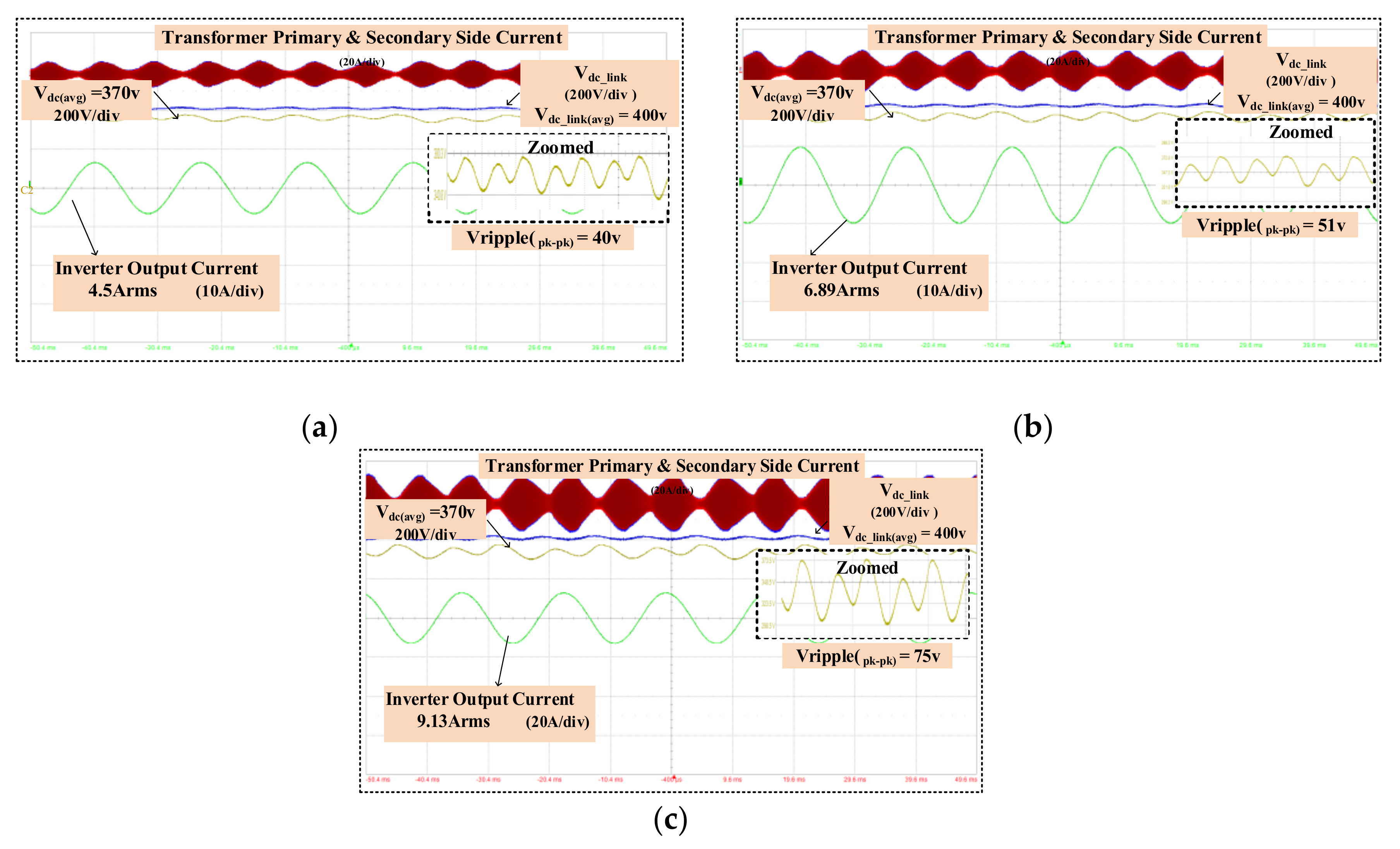
5.1. Simulation Results

In order to verify the performance of the proposed method a PSIM simulation is performed. The circuit parameters and system specification can be found in Table 1 and Table 3. It is desirable to limit the input ripple to be as small as possible to minimize the losses caused by the interactions among the renewable energy source, the double line frequency ripple and the power rating of the components used in the converter such as the transformer and the switches [24,25]. Here, the input capacitance value is 200 µF. Since the double line frequency ripple at the DC link side is allowed up to 60 Vp-p (7.5% variation of the DC link voltage) at 5 kW, the required DC link capacitance is just 400 uF in accordance with Equation (5). The double line frequency ripple can be further reduced if a larger DC link capacitance is used.
Figure 10 shows simulation results with and without the double line frequency ripple elimination control at 1 kW and 5 kW in order to show the effectiveness of the proposed method. Figure 10a,b shows simulation results when the proposed algorithm is not applied. It can be clearly seen that the voltage at the DC source includes a 120 Hz ripple of with an amplitude of 40 Vp-p and 110 Vp-p at 1 kW and 5 kW, respectively. The DC-link voltage also has a double line frequency ripple component of 18 Vp-p and 60 Vp-p at 1 kW and 5 kW, respectively. Figure 10c,d show PSIM simulation results when the proposed algorithm is applied. It can be observed from Figure 10c,d that the 120 Hz ripple is effectively suppressed by the proposed method and that only a 3 Vp-p ripple at 1 kW and a 6 Vp-p ripple at 5 kW remains at the DC source, which is less than 2% of the DC input voltage. Although the amplitude of the double line frequency ripple at the DC link is the same as before, the inverter can successfully generate a 60 Hz output current over the entire load range.

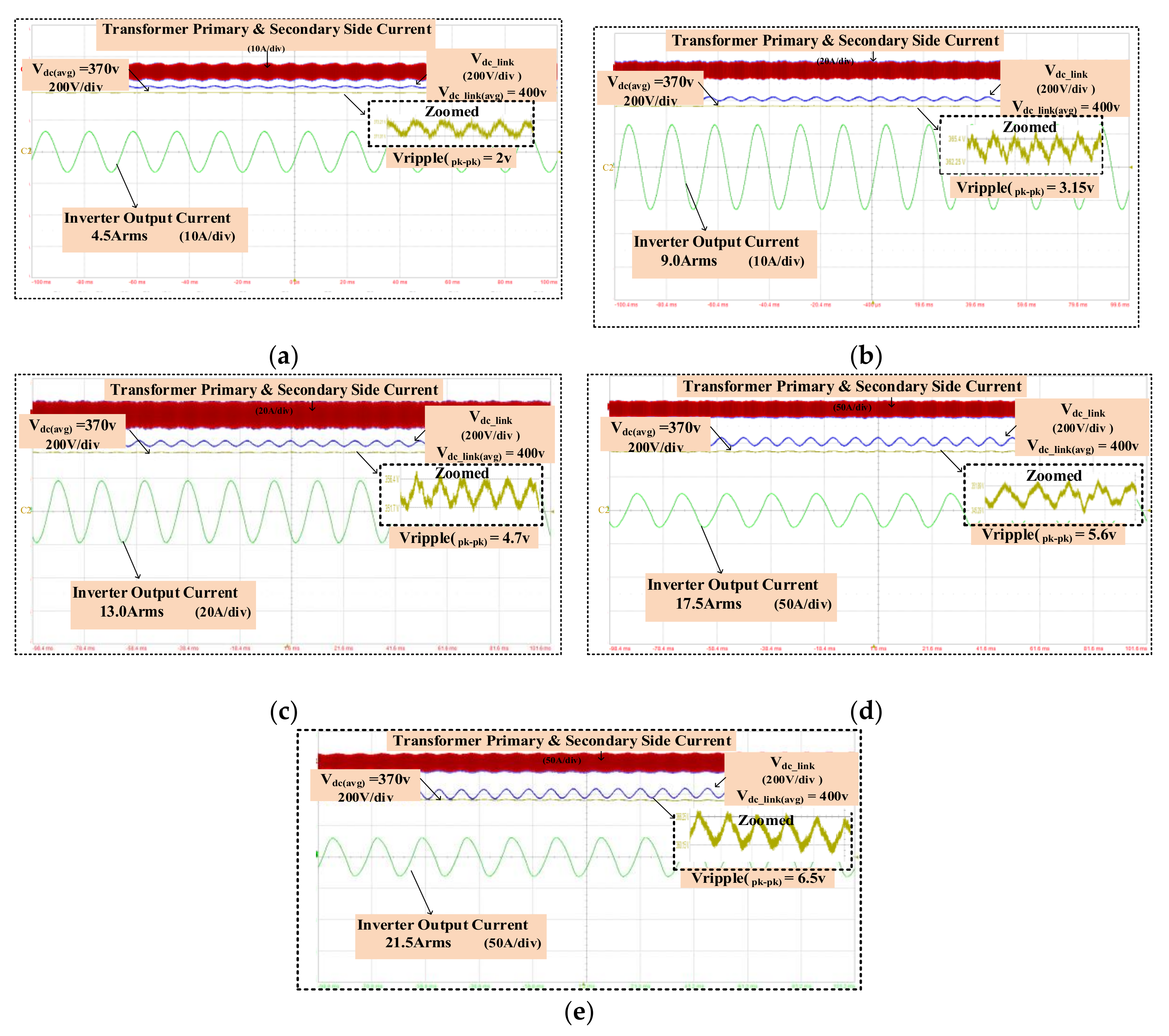
5.2. Experimantal Results

For experimental verification of the proposed method, a DAB converter and a single phase full-bridge inverter have been implemented as shown in Figure 11. Here, a TeraSAS ETS (600/17) photovoltaic simulator has been used as a DC Source since it can allow a 120 Hz ripple at its input with a very small output capacitance. The DAB converter and the VSI inverter are controlled by a DSP TMS320F28335. The proposed double line frequency elimination technique has been implemented in the DSP for the DAB converter.
In order to show the effectiveness of the proposed method, experiments are performed with and without the proposed double line frequency ripple elimination algorithm. Figure 12 shows experimental waveforms of the two stage DC/AC power conversion system without the proposed double line frequency ripple elimination algorithm. The waveforms from top to bottom in Figure 12 are Ip, Is, VDC_link, VDC and IL, which show the primary and secondary current of the transformer, DC link voltage, DC input voltage and inverter output current, respectively.
Figure 12 clearly indicates that the voltage at the DC input side and the current at the primary and secondary side of the transformer all have a 120 Hz ripple component. When the power of the converter is increased, the amplitude of the ripple is also increased. Here, experiments are performed up to a 2.0 kW output power since the DC source PV simulator turns off due to the double line frequency ripple when the power exceeds 2.0 kW.
Experimental results obtained with the proposed double line frequency ripple elimination control are obtained at 1 kW, 2 kW, 3 kW, 4 kW and 5 kW in order to verify the validity of the proposed control method. Figure 13 illustrates results when the proposed method is enabled. It can be seen from Figure 13 that the 120 Hz ripple is effectively suppressed by the proposed method. It can also be observed that the currents at both sides of the transformer are free of low frequency ripple.
In Figure 13, the maximum ripple at the DC source is only 6.5 Vp-p at 5 kW, which proves that the ripple at the input is effectively suppressed by the proposed control algorithm. The ripple can be eliminated from the input side with only a 200 μF capacitance at the DC input side. In addition, the capacitance value used at the DC link is only 400 μF. Furthermore, experimental results show that the controller successfully regulates 400 V at the DC link to obtain AC 220 Vrms at the inverter output.
In order to obtain a 6.5 Vp-p ripple at the DC input source without the double line frequency ripple elimination method, the required capacitance is 5000 μF according to Equation (5). This is 25 times larger than that of the proposed system (200 μF). The reduction in the DC source side decoupling capacitance is calculated as 96%. On the other hand, only a 400 uF capacitor can be used at the DC link side if a peak ripple voltage of 30 V is allowed.
Figure 14a shows a comparison chart for the double line frequency ripple with and without the proposed method at 1 kW, 1.5 kW and 2 kW. As shown in Figure 14, the double line frequency ripple can be effectively suppressed by the proposed method up to 95.8%.
Table 4 shows a comparison of several double line frequency ripple reduction methods in terms of the percentage of the ripple reduction, the required capacitance and the volume of the capacitor used. It is clearly shown in Table 4 that the proposed method is outstanding among the methods developed so far in terms of capacitor volume, ripple reduction and capacitance reduction.

6. Conclusions

This paper has presented a novel double line frequency ripple elimination method for two-stage single-phase DC-AC power conversion systems. With the proposed ripple elimination method, the input capacitance of the front-end dc-dc converter can be reduced by 96% and the double line frequency ripple can be suppressed by up to 95.8%. The main advantage of the proposed method is that it does not require any additional circuits to reduce the ripple at the DC source side. Thanks to the ripple elimination capability of the proposed technique, it can achieve several advantages such as elimination of the power loss associated with ripple current, reduction in the rating of the components used in the circuit, and prolonged lifetime of the power conversion system owing to the use of film capacitors. In addition, the volume and cost of the converter can be further reduced due to the small capacitance value required to maintain the DC link. The validity and the feasibility of the proposed control method have been verified by experimental results with a 5 kW two-stage single-phase inverter.

Author Contributions

S.A. proposed the idea of the paper. The formal analysis and prototype were designed by S.A.; The paper was written by S.A., and reviewed by H.-H.L. and S.A. All the authors were involved in giving the final shape to this manuscript. Moreover, this work was supervised by W.C. All authors have read and agreed to the published version of the manuscript.

Funding

This research was supported by Korea Electric Power Corporation. (Grant number: R17XA05-42).

Conflicts of Interest

The authors declare no conflict of interest.

References

  1. Kjaer, S.; Pedersen, J.; Blaabjerg, F. A Review of Single-Phase Grid-Connected Inverters for Photovoltaic Modules. IEEE Trans. Ind. Appl. 2005, 41, 1292–1306. [Google Scholar] [CrossRef]
  2. Riedel, J.; Holmes, D.G.; McGrath, B.; Teixeira, C.A. Active Suppression of Selected DC Bus Harmonics for Dual Active Bridge DC-DC Converters. IEEE Trans. Power Electron. 2016, 32, 1. [Google Scholar] [CrossRef]
  3. Akagi, H.; Yamagishi, T.; Tan, N.M.L.; Kinouchi, S.-I.; Miyazaki, Y.; Koyama, M. Power-Loss Breakdown of a 750-V 100-kW 20-kHz Bidirectional Isolated DC–DC Converter Using SiC-MOSFET/SBD Dual Modules. IEEE Trans. Ind. Appl. 2014, 51, 420–428. [Google Scholar] [CrossRef]
  4. Segaran, D.; Holmes, D.G.; McGrath, B. High-performance bi-directional AC-DC converters for PHEV with minimised DC bus capacitance. In Proceedings of the IECON 2011 37th Annual Conference of the IEEE Industrial Electronics Society, Melbourne, VIC, Australia, 7–10 November 2011; pp. 3620–3625. [Google Scholar]
  5. Antivachis, M.; Anderson, J.A.; Bortis, D.; Kolar, J.W. Analysis of a synergetically controlled two-stage three-phase DC/AC buck-boost converter. CPSS TPEA 2020, 5, 34–53. [Google Scholar] [CrossRef]
  6. Hu, H.; Harb, S.; Kutkut, N.; Batarseh, I.; Shen, Z.J. A Review of Power Decoupling Techniques for Microinverters With Three Different Decoupling Capacitor Locations in PV Systems. IEEE Trans. Power Electron. 2012, 28, 2711–2726. [Google Scholar] [CrossRef]
  7. Dod, S. Reliability Prediction of Electronic Equipment; MIL-HDBK-217D; Rome Air Development Center Griffss AFB: New York, NY, USA, 1982. [Google Scholar]
  8. Sun, Y.; Liu, Y.; Su, M.; Xiong, W.; Yang, J. Review of activepower decoupling topologies in single-phase systems. IEEE Trans. Power Electron. 2016, 31, 4778–4794. [Google Scholar]
  9. Ma, X.; Wang, B.; Zhao, F.; Qu, G.; Gao, D.; Zhou, Z. A high power low ripple high dynamic performance DC power supply based on thyristor converter and active filter. In Proceedings of the IEEE 2002 28th Annual Conference of the Industrial Electronics Society, IECON 02, Sevilla, Spain, 5–8 November 2003; Volume 2, pp. 1238–1242. [Google Scholar]
  10. Irfan, M.S.; Ahmed, A.; Park, J.-H.; Seo, C. Current-Sensorless Power-Decoupling Phase-Shift Dual-Half-Bridge Converter for DC–AC Power Conversion Systems Without Electrolytic Capacitor. IEEE Trans. Power Electron. 2017, 32, 3610–3622. [Google Scholar] [CrossRef]
  11. Liu, C.; Johnson, A.; Lai, J.-S. A novel three-phase high-power soft switched DC/DC converter for low voltage fuel cell applications. IEEE Trans. Ind. Appl. 2004, 3, 1365–1371. [Google Scholar] [CrossRef]
  12. Itoh, J.; Hayashi, F. Ripple Current Reduction of a Fuel Cell for a Single-Phase Isolated Converter Using a DC Active Filter with a Center Tap. IEEE Trans. Power Electron. 2010, 25, 550–556. [Google Scholar] [CrossRef]
  13. Liu, C.; Lai, J.-S. Low Frequency Current Ripple Reduction Technique with Active Control in a Fuel Cell Power System with Inverter Load. IEEE Trans. Power Electron. 2006, 22, 1429–1436. [Google Scholar] [CrossRef]
  14. Qian, Z.; Abdel-Rahman, O.; Hu, H.; Batarseh, I. An integrated three-port inverter for stand-alone PV applications. IEEE Energy Convers. Congr. Expo. 2010, 1471–1478. [Google Scholar] [CrossRef]
  15. Liu, D.; Li, H. A ZVS Bi-Directional DC–DC Converter for Multiple Energy Storage Elements. IEEE Trans. Power Electron. 2006, 21, 1513–1517. [Google Scholar] [CrossRef]
  16. Li, W.; Xiao, J.; Zhao, Y.; He, X. PWM Plus Phase Angle Shift (PPAS) Control Scheme for Combined Multiport DC/DC Converters. IEEE Trans. Power Electron. 2011, 27, 1479–1489. [Google Scholar] [CrossRef]
  17. Möhr, M.; Fuchs, F.-W. Current-Fed Full Bridge Converters for Fuel Cell Systems Connected to the Three Phase Grid. In Proceedings of the 2006 1st International Conference on Nano-Networks and Workshops, Paris, France, 6–10 November 2006; pp. 4313–4318. [Google Scholar]
  18. Cai, W.; Liu, B.; Duan, S.; Jiang, L. An Active Low-Frequency Ripple Control Method Based on the Virtual Capacitor Concept for BIPV Systems. IEEE Trans. Power Electron. 2013, 29, 1733–1745. [Google Scholar] [CrossRef]
  19. Hu, H.; Harb, S.; Fang, X.; Zhang, D.; Zhang, Q.; Shen, Z.J.; Batarseh, I. A Three-port Flyback for PV Microinverter Applications with Power Pulsation Decoupling Capability. IEEE Trans. Power Electron. 2012, 27, 3953–3964. [Google Scholar] [CrossRef]
  20. Hu, H.; Harb, S.; Kutkut, N.; Batarseh, I.; Shen, Z.J. Power decoupling techniques for micro-inverters in PV systems-a review. IEEE Energy Convers. Congr. Expo. 2010, 3235–3240. [Google Scholar] [CrossRef]
  21. Li, Q.; Wolfs, P.J. A Review of the Single Phase Photovoltaic Module Integrated Converter Topologies With Three Different DC Link Configurations. IEEE Trans. Power Electron. 2008, 23, 1320–1333. [Google Scholar] [CrossRef] [Green Version]
  22. Rodriguez, A.; Vazquez, A.; Lamar, D.G.; Hernando, M.M.; Sebastian, J. Different Purpose Design Strategies and Techniques to Improve the Performance of a Dual Active Bridge With Phase-Shift Control. IEEE Trans. Power Electron. 2015, 30, 790–804. [Google Scholar] [CrossRef]
  23. Demetriades, G.D. On Small-Signal Analysis and Control of the Single- and Dual-Active Bridge Topologies. Ph.D. Thesis, The Royal Institute of Technology, Stockholm, Sweden, 2005. [Google Scholar]
  24. Choi, W.; Howze, J.; Enjeti, P. Development of an equivalent circuit model of a fuel cell to evaluate the effects of inverter ripple current. J. Power Sources 2006, 158, 1324–1332. [Google Scholar] [CrossRef]
  25. Kim, W.; Duong, V.-H.; Nguyen, T.-T.; Choi, W. Analysis of the effects of inverter ripple current on a photovoltaic power system by using an AC impedance model of the solar cell. Renew. Energy 2013, 59, 150–157. [Google Scholar] [CrossRef]
  26. He, D.; Cai, W.; Yi, F. A power decoupling method with small capacitance requirement based on single-phase quasi-Z-source inverter for DC microgrid applications. In Proceedings of the 2016 IEEE Applied Power Electronics Conference and Exposition (APEC), Long Beach, CA, USA, 20–24 March 2016; pp. 2599–2606. [Google Scholar]
  27. Xu, S.; Shao, R.; Chang, L.; Mao, M. Single-Phase Differential Buck–Boost Inverter With Pulse Energy Modulation and Power Decoupling Control. IEEE J. Emerg. Sel. Top. Power Electron. 2018, 6, 2060–2072. [Google Scholar] [CrossRef]
  28. Liu, X.; Li, H.; Wang, Z. A Fuel Cell Power Conditioning System With Low-Frequency Ripple-Free Input Current Using a Control-Oriented Power Pulsation Decoupling Strategy. IEEE Trans. Power Electron. 2013, 29, 159–169. [Google Scholar] [CrossRef]
  29. Liu, Y.; Sun, Y.; Su, M. A Control Method for Bridgeless Cuk/Sepic PFC Rectifier to Achieve Power Decoupling. IEEE Trans. Ind. Electron. 2017, 64, 7272–7276. [Google Scholar] [CrossRef]
  30. Lyu, X.; Ren, N.; Li, Y.; Cao, N. A SiC-Based High Power Density Single-Phase Inverter With In-Series and In-Parallel Power Decoupling Method. IEEE J. Emerg. Sel. Top. Power Electron. 2016, 4, 893–901. [Google Scholar] [CrossRef]
  31. Wang, H.; Chung, H.S.-H.; Liu, W. Use of a Series Voltage Compensator for Reduction of the DC-Link Capacitance in a Capacitor-Supported System. IEEE Trans. Power Electron. 2013, 29, 1163–1175. [Google Scholar] [CrossRef] [Green Version]
  32. Tang, Y.; Blaabjerg, F.; Loh, P.C.; Jin, C.; Wang, P. Decoupling of Fluctuating Power in Single-Phase Systems Through a Symmetrical Half-Bridge Circuit. IEEE Trans. Power Electron. 2015, 30, 1855–1865. [Google Scholar] [CrossRef]
  33. Xia, Y.; Roy, J.; Ayyanar, R. A Capacitance-Minimized, Doubly Grounded Transformer less Photovoltaic Inverter With Inherent Active-Power Decoupling. IEEE Trans. Power Electron. 2017, 32, 5188–5201. [Google Scholar] [CrossRef]
  34. Roy, J.; Xia, Y.; Ayyanar, R.; Ayyanar, R. Half-Bridge Voltage Swing Inverter With Active Power Decoupling for Single-Phase PV Systems Supporting Wide Power Factor Range. IEEE Trans. Power Electron. 2019, 34, 7450–7461. [Google Scholar] [CrossRef]
  35. Shi, Y.; Li, R.; Xue, Y.; Li, H. High-Frequency-Link Based Grid-tied PV System with Small DC-link Capacitor and Low-frequency Ripple-free Maximum Power Point Tracking. IEEE Trans. Power Electron. 2015, 31, 1. [Google Scholar] [CrossRef]
Figure 1. Conventional power decoupling methods: (a) methods in [14,15,16]; (b) method in [12]; (c) method in [8].
Electronics 09 00931 g001
Figure 2. Two-stage single-phase DC/AC converter with the proposed ripple current control algorithm.
Electronics 09 00931 g002
Figure 3. Key waveforms of a DAB converter.
Electronics 09 00931 g003
Figure 4. Power transfer characteristics of a DAB according to the duty cycle.
Electronics 09 00931 g004
Figure 5. Simplified small signal average model of a DAB (Dual Active Bridge) converter.
Electronics 09 00931 g005
Figure 6. Comparison of Bode plots of a DAB converter drawn by MATLAB and PSIM.
Electronics 09 00931 g006
Figure 7. Control loop block diagram representation of a DAB converter.
Electronics 09 00931 g007
Figure 8. Control block diagrams: (a) proposed DAB converter control; (b) double line frequency ripple elimination loop; (c) DC link voltage control with the double line frequency ripple elimination.
Electronics 09 00931 g008
Figure 9. Bode plot: (a) TVDC; (b) TVDC_link.
Electronics 09 00931 g009
Figure 10. Simulation results: (a) without the proposed control method at 1 kW; (b) without the proposed control method at 5 kW; (c) with the proposed control method at 1 kW; (d) with the proposed control method at 5 kW.
Electronics 09 00931 g010
Figure 11. Experimental setup of a 5 kW two-stage DC/AC converter.
Electronics 09 00931 g011
Figure 12. Experimental waveforms without the proposed double line frequency ripple elimination method (from top to bottom: transformer primary & secondary current, dc-link voltage, DC input voltage and inverter output current): (a) 1 kW; (b) 1.5 kW; (c) 2.0 kW.
Electronics 09 00931 g012
Figure 13. Experimental waveforms with the proposed double line frequency ripple elimination method (from top to bottom: transformer primary & secondary side current, dc-link voltage, input source voltage, inverter output current): (a) 1 kW; (b) 2 kW; (c) 3 kW; (d) 4 kW; (e) 5 kW.
Electronics 09 00931 g013
Figure 14. (a) Comparison of the ripple reduction with and without the double line frequency ripple controller. (b) Prototype hardware efficiency profile with respect to different load power.
Electronics 09 00931 g014
Table 1. Specification of the System.
DesignatorParametersValues
VDCPV Simulator Voltage380 V
VDC_linkDC-Link Voltage400 Vrms
VrmsInverter Output Voltage220 Vrms
PoInverter Output Power5 kW
Table 2. Component for the Hardware Test.
ComponentManufacturerPart Number
MosfetRohmSCH2080 KE
Filim CapacitorPanasonic
Magnetic CoreChangsungPQ72/52
Gate DriverSilicon LabSi8275
Table 3. Design Parameters.
DesignatorParametersValues
CDCDC-Source Capacitance200 µF
CDC_linkDC-Link Capacitance400 µF
CBlockingDC-Blocking Capacitance8 µF
LlkLeakage Inductance20.71 µH
nTransformer turns ratio1:1
FsSwitching Frequency (DAB)100 kHz
FgSwitching Frequency (Inverter)10 kHz
Table 4. Comparison of the reduction of 120 Hz ripple at the DC input.
Input Capacitor ValuesInput Capacitor Reduction (%)Ripple Reduction at DC input (%)DC Input Voltages (V)Ripple at the DC-Link (Vp-p)PowerAdditional Hardware RequiredC × V/Power (μF×kV/kW)
[10]2 × 50 µF64NP 120020425 WYes47.05
[18]100 µF7494.3400NP2 kWYes20
[26]2 × 100 µF909015050500 WNo60
[27]2 × 30 µF9050100150400 WNo15
[28]320 µF90.458.6200501 kWNo40
[29]100 µF78NP 1100130500 WNo20
[30]100 µF896845010.52 kWNo22.5
[31]120 µF829240010.81 kWYes48
[32]2 × 90 µF74.2191380101 kWYes68.4
[33]9 × 5 µF689711002803 kWNo16.5
[34]2 × 12 µF/30 µF97NP1651501 kWNo27
[35]30/120/10 µF95961501464 kWYes32
(Proposed)2 × 100 µF9695380605 kWNo15.2
1 NP (Not Provided).

