Article

An Energy-Efficient and Fast Scheme for Hybrid Storage Class Memory in an AIoT Terminal System

1
Institute of Microelectronics of the Chinese Academy of Sciences, Beijing 100029, China
2
School of Electronic, Electrical and Communication Engineering, University of Chinese Academy of Sciences, Beijing 100049, China
*
Author to whom correspondence should be addressed.
Electronics 2020, 9(6), 1013; https://doi.org/10.3390/electronics9061013
Submission received: 20 May 2020 / Revised: 13 June 2020 / Accepted: 15 June 2020 / Published: 17 June 2020
(This article belongs to the Section Computer Science & Engineering)

Abstract

:
Conventional main memory can no longer meet the requirements of low energy consumption and massive data storage in an artificial intelligence Internet of Things (AIoT) system. Moreover, the efficiency is decreased due to the swapping of data between the main memory and storage. This paper presents a hybrid storage class memory system to reduce the energy consumption and optimize IO performance. Phase change memory (PCM) brings the advantages of low static power and a large capacity to a hybrid memory system. In order to avoid the impact of poor write performance in PCM, a migration scheme implemented in the memory controller is proposed. By counting the write times and row buffer miss times in PCM simultaneously, the write-intensive data can be selected and migrated from PCM to dynamic random-access memory (DRAM) efficiently, which improves the performance of hybrid storage class memory. In addition, a fast mode with a tmpfs-based, in-memory file system is applied to hybrid storage class memory to reduce the number of data movements between memory and external storage. Experimental results show that the proposed system can reduce energy consumption by 46.2% on average compared with the traditional DRAM-only system. The fast mode increases the IO performance of the system by more than 30 times compared with the common ext3 file system.

1. Introduction

The emergence of the Internet of Thing (IoT) has given rise to many opportunities and challenges. In the early days, many IoT devices could only collect and send data to the cloud for analysis. However, the increasing computing capacity of today’s devices allows them to perform complex computations on-site [1,2]. As the processing capabilities of IoT devices are gradually increasing, the applications in IoT devices have become increasingly complicated. Recently, complex artificial intelligence applications can also be processed in edge devices called artificial intelligence Internet of Things (AIoT) devices and systems. IoT devices are usually self-powered, using batteries or even energy harvesting [3], so they need to be on low power for long standby time. AIoT devices are used to execute image and video applications with large memory footprints. Unfortunately, the conventional DRAM-based main memory incurs problems, such as high energy consumption and small density, which have to be addressed before large amounts of data can be processed efficiently in DRAM-only memory [4].
As DRAM suffers from limited scalability and high power leakage, the emergence of many new non-volatile memories, such as PCM [5,6], spin-transfer torque magnetic random access memory (STT-MRAM) [7], resistive random access memory (RRAM) [8], and 3D-Xpoint [9], provides new solutions for a main memory architecture. These byte-addressable memories are non-volatile, achieve low static energy consumption, and have a high density.
In particular, PCM is considered to be the most likely non-volatile memory to replace DRAM as the main memory because of its special characteristics. PCM has small-sized cells and excellent scalability within the complementary metal oxide semiconductor (CMOS) fabrication process, which makes PCM have a higher density than DRAM [10]. Thus, it is possible to produce a PCM chip with larger capacity. The most attractive advantage of PCM is that it does not need to be refreshed because it is non-volatile, making the PCM have a low static energy consumption. On the other hand, the refresh mechanism of traditional DRAM main memory has caused large energy consumption. Therefore, some studies have attempted to use PCM to completely replace DRAM as the main memory [11].
Unfortunately, compared to DRAM, the PCM still has some disadvantages including longer write latency, higher write energy and limited write endurance. The longer write latency of PCM affects the performance of memory system. The higher write energy leads to the large energy consumption of the memory system in the cases with intensive write operations. A PCM cell can only sustain a limited number of write operations which is generally 108. The endurance of PCM is worse than that of DRAM (1015), but is better than NAND Flash (105) [10]. Hence, the PCM could also be used in hybrid flash-PCM architectures to counter some of the disadvantages of flash memory [12].
Consequently, the hybrid memory systems have been proposed. This would allow large amounts of energy to be saved as compared to full DRAM implementation. For instance, the common DRAM-PCM hybrid memory system comprised of both DRAM and PCM in the physical address space can be directly accessed by processors to achieve the low access latency and high endurance of DRAM, while taking advantage of PCM’s large capacity and low static power.
In order to exploit the low energy and high speed of DRAM write, many previous works have studied hybrid memory management in different ways. Some software-managed hybrid memory systems exploit operating systems to manage pages between DRAM and non-volatile memories [13,14,15]. A hardware–software mechanism for hybrid memory management migrates multiple pages concurrently without significantly affecting the memory performance [16]. In addition, using an extended on-chip cache policy is also a viable method to enhance the performance of hybrid memory [17]. Some hardware-based management systems use a modified memory controller to manage the pages in hybrid memory. Hardware-managed swap techniques generally induce a lower overhead than software-managed ones [18]. However, both software and hardware methods are rarely optimized for IoT devices. The diversity of IoT applications makes it difficult to present a general method for all kinds of situations [1]. This paper focuses on the applications of image processing with large memory footprints. A fast and energy efficient scheme is proposed to provide a novel solution for applications of image processing in AIoT devices.
The remainder of this paper is organized as follows. Section 2 presents the architecture of hybrid storage class memory (HSCM) and a migration scheme for applications of image processing. Section 3 introduces a fast mode to improve the IO performance of the system. In Section 4, the experimental results are described. Finally, Section 5 concludes this paper.

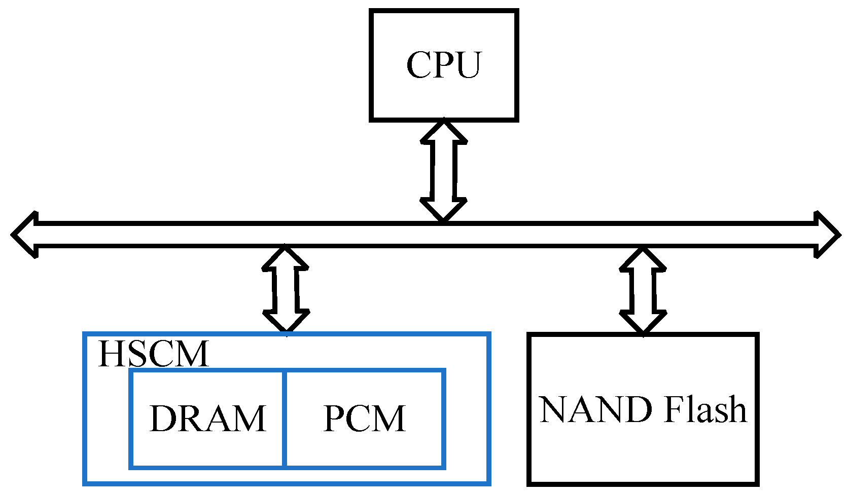
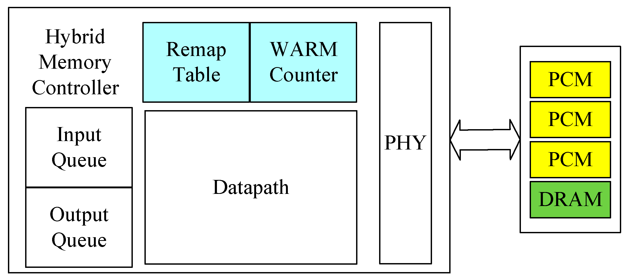
2. Hybrid Storage Class Memory

Most non-volatile memories incur high access latency, high dynamic energy consumption, and limited write endurance. To address these weaknesses, a hybrid memory system comprised of both DRAM and non-volatile memory has been proposed. We use DRAM and PCM to compose hybrid storage class memory. Notably, the DRAM and PCM are in a unified address space managed by the hybrid memory controller. The architecture of hybrid storage class memory is shown in Figure 1.

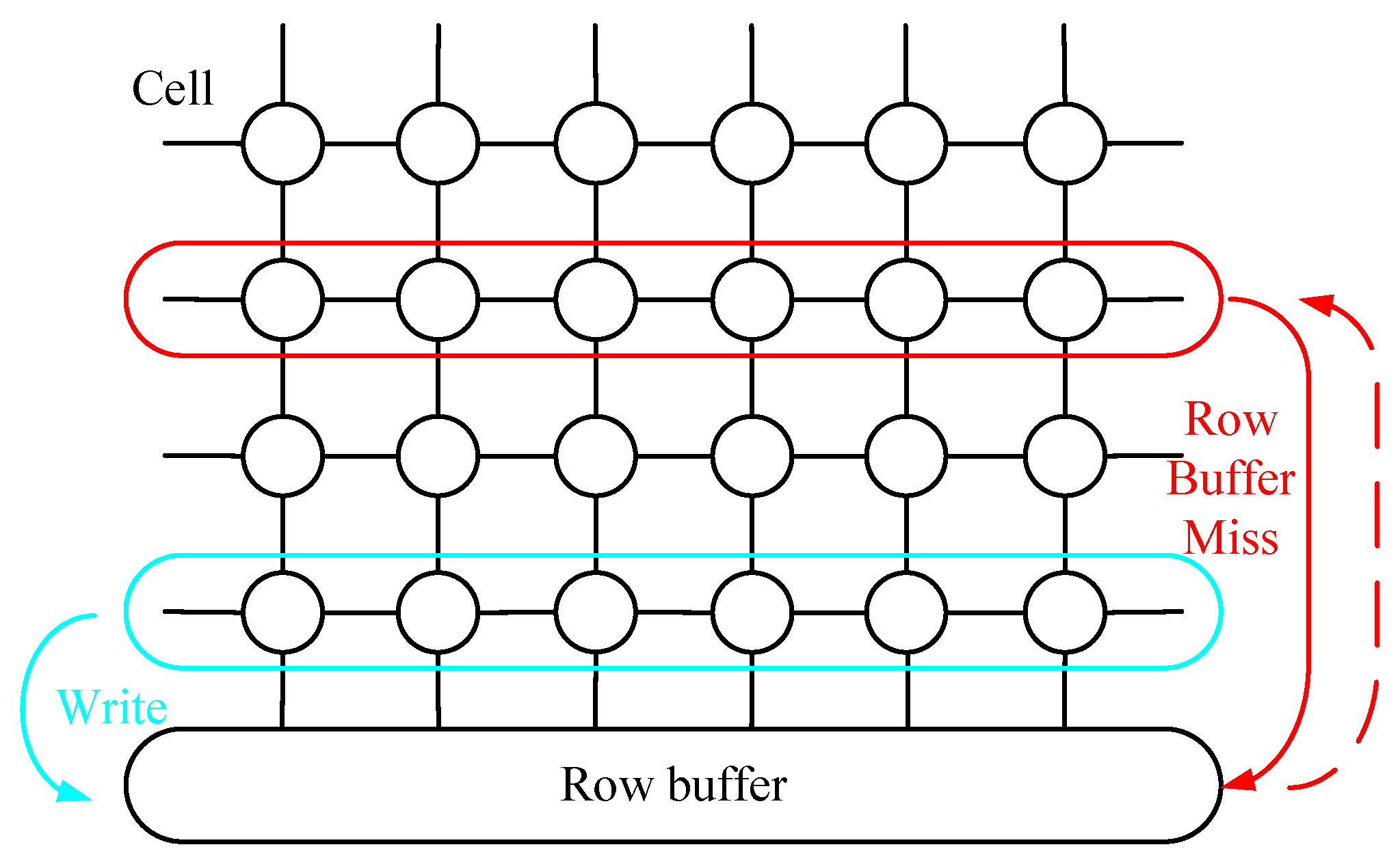
2.1. Row Buffer Architecture

For conventional DRAM-based main memory, the row buffer serves as a cache for the most recently accessed row. In our study, both DRAM and PCM banks utilize the row buffer architecture for better compatibility. Row buffer locality refers to the repeated reference to a row, while its contents are in the row buffer. The open page strategy [19] can be applied to the memory system with a row buffer architecture. Memory requests to data with a high row buffer locality are served efficiently without having to frequently re-activate the memory cell array.
The open page strategy is implemented in HSCM. When the controller receives a request, if the row buffer hits, the corresponding data is read or written directly from it; otherwise, the original row is closed by a precharge. The data in the target row should be loaded into the row buffer. The row buffer then reads the required data and waits for the next operation. Figure 2 shows the open page strategy in the row buffer.
The biggest difference between PCM and DRAM is whether it is non-volatile. When the row buffer miss happens, all the data in the DRAM row buffer must be written back to the original row by the precharge, and the other row can then be loaded into the row buffer. By contrast, read operations in PCM are non-destructive. The read operation can obtain a better performance by reducing the number of precharges. Therefore, in the case of a row buffer miss, the memory controller can check whether the content of the current row buffer has been revised. If it is changed, the data need to be written back to the original row; otherwise, the data in the current row buffer can be discarded. This can reduce the energy and latency of the PCM. However, with PCM, the energy consumption and latency of the precharge are still much higher than with DRAM. According to the analysis, the write with the row buffer miss in PCM is worse than in DRAM.

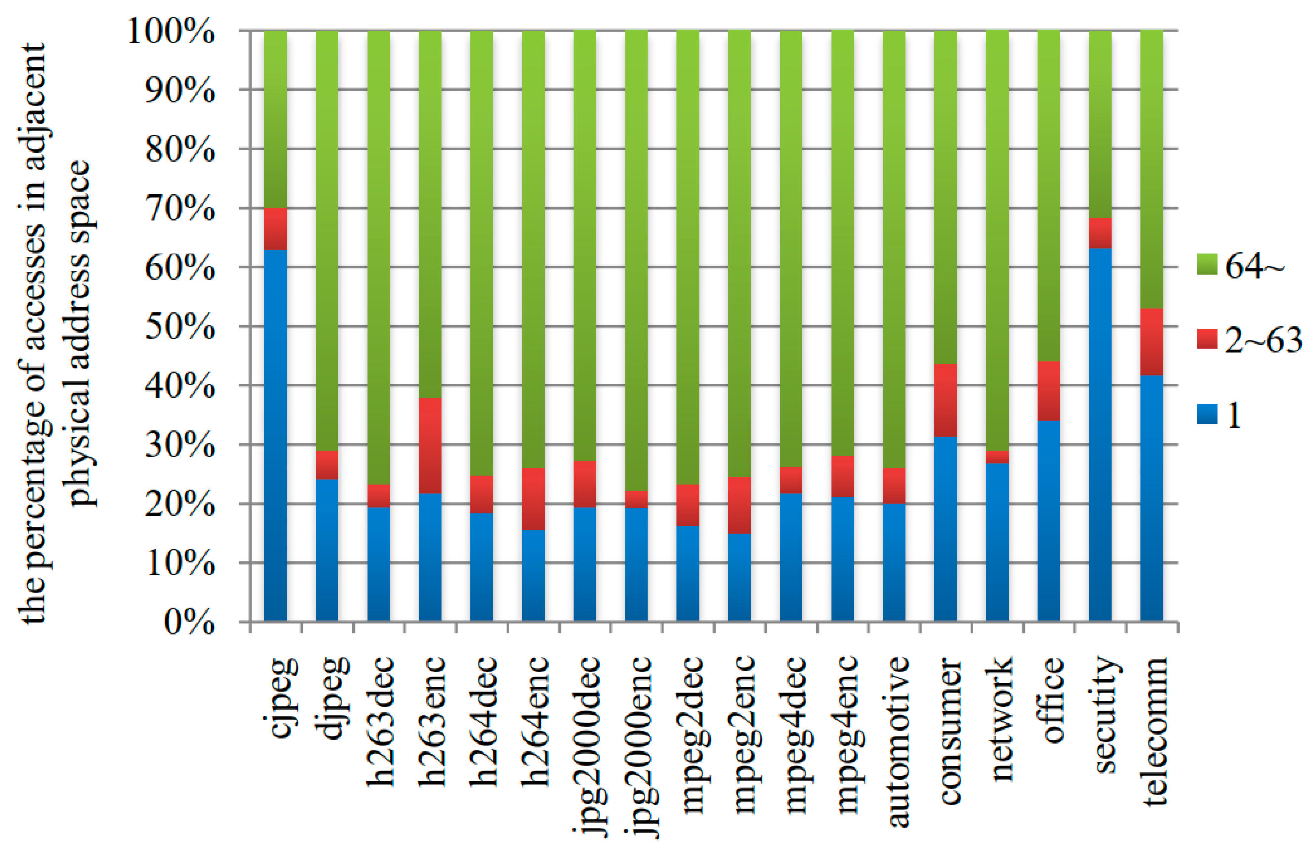
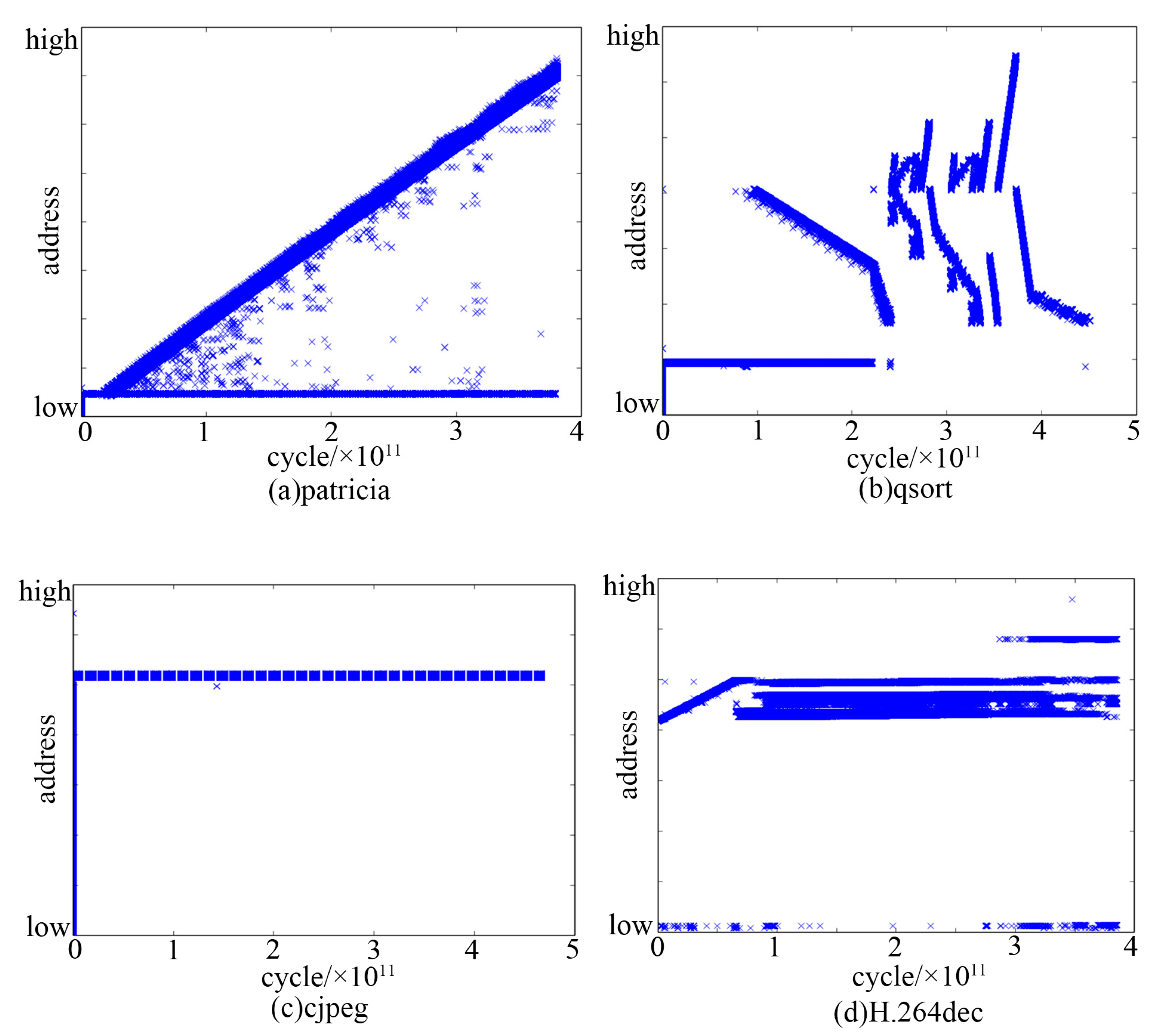
2.2. Memory Access Pattern in IoT Applications

Different applications have different memory access patterns. For the purpose of developing a more targeted scheme, the memory access patterns of benchmarks for IoT applications [20,21] are studied. The memory access pattern provides a reference for further research and helps to design a more workable strategy. As can be seen in Figure 3, we have evaluated the space locality of benchmarks by counting the proportion of different intervals in the address space among all memory accesses [22]. The memory access patterns are obtained through the gem5 simulator [23].
The interval refers to the address space between two consecutive accesses. Figure 3 depicts that more than 15% of accesses are in an adjacent physical address space (where the interval is 1). Considering that the capacity of a row is larger than a cache line, the larger intervals also have some locality. For example, when the interval between two accesses is less than 64 (the cache line size is 64 bytes, and the row size is 64 bytes × 64 = 4 kB), it is considered that there is a high probability that these accesses are in the same row. In this case, the row buffer hit will happen in the memory with an open page strategy. On the other hand, when the interval is more than 64, a row buffer miss is possible. Figure 3 shows that the IoT applications have spatial locality. In particular, the spatial localities of cjpeg and security are better than the other applications.
The concentration of memory access is an important factor in a memory access pattern. The intensive address access is conducive to the design of an appropriate algorithm. As can be seen in Figure 4, some representative memory access patterns are illustrated. The x-axis denotes the cycle (time) of writing in memory, and the y-axis denotes the address value (from low to high). In Figure 4a,b, patricia and qsort represent two kinds of write access patterns in IoT applications. cjpeg and H.264dec represent the write access patterns in applications of image processing in Figure 4c,d, respectively.
As shown in Figure 4a,b, addresses accessed by write operations are scattered, although the patricia in Figure 4a is distributed with some regularity. What can be clearly seen in Figure 4b is the irregular access in qsort. This means that applications such as qsort are difficult to solve with a simple algorithm due to their unique memory access patterns. In some cases, as shown in Figure 4c,d, in applications of image processing, because the IoT devices are usually used to monitor the environment, the pictures and videos have a good similarity within a certain period of time. Consequently, most write operations concentrate on a few addresses. If this part of write operation is concentrated on the PCM, it will adversely affect the energy consumption and the performance of the memory system. Moreover, the intensive write operations are not conducive to extending the life of PCM. Therefore, a strategy that can transfer these intensive write operations to DRAM should be proposed.

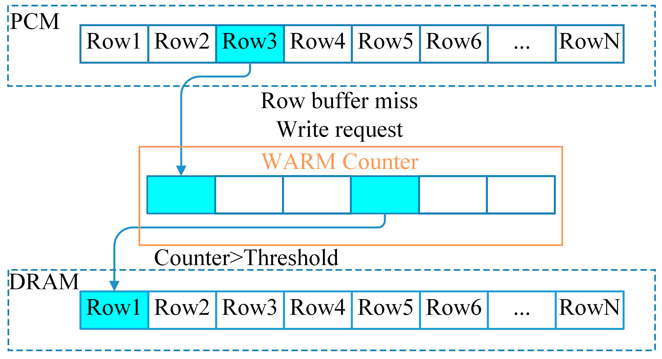
2.3. Row Buffer Locality and Write Aware Scheme

According to the analysis in Section 2.1 and Section 2.2, a novel memory controller design is proposed to improve hybrid memory performance and energy efficiency. The memory controller combines memory access characteristics with row buffer locality as the basis for row migration. A write-aware and row buffer miss (WARM) counter is implemented to evaluate the characteristics of each row and decide whether the row should be migrated. A remap table records the addresses of rows that have been migrated. Due to the remap table, when the rows are accessed again, the correct data can be obtained. The WARM counter module and remap table module are integrated in the memory controller. The architecture of the modified memory controller is shown in Figure 5. The initial ratio of DRAM and PCM is set to 1:3.
Different access behaviors will have different effects on the system. For example, if a row is written in the PCM, two cases are possible. The first case is that the next row accessed is the same row. In this case, whether the operation is write or read, it will happen directly in the row buffer under the open page strategy. The precharge will not occur during this period until the access to another row arrives. The second case is that the next row accessed is different from the current one, which indicates that a row buffer miss occurred. In this case, the current row will be precharged immediately. Compared with the first case, the second is worse in PCM because of the higher energy consumption and latency. However, in both cases, the write operation will eventually lead to a precharge.
Previous work on hybrid memory systems observed that the latency of a row buffer hit is similar in different memories, while the latency of a row buffer miss is generally much higher in PCM [24]. When a row buffer miss occurs in PCM, if data in the row buffer are modified, this row should be precharged. In this case, PCM consumes more energy because of the row buffer miss.
Based on the above observations and analysis, a row buffer locality and write aware scheme for HSCM is proposed, integrating the row migration algorithm in the WARM counter in the hybrid memory controller. The scheme uses a WARM counter to select the rows that need to be migrated. The rows in the PCM where write operations frequently occur will cause more precharge operations, resulting in a poor performance of energy consumption and latency. In addition, rows with poor row buffer locality will bring more data exchange in the row buffer, and the performance of this exchange in PCM is also a major factor that reduces memory system performance. We need to consider the impact of these two factors in the migration strategy. In other words, the rows with more write requests and buffer misses should be migrated from PCM to DRAM. In addition, a memory address mapping table is maintained to record the new addresses after the rows are migrated. The migration between memory devices is managed by hardware, and is transparent to the operating system.
Since the hardware and software resources in current IoT devices are limited, the algorithm using a large amount of hardware or software resources is not suitable for our AIoT terminal system. In [18], the rank-based page placement (RaPP) algorithm maintains multiple queues to find out pages with intensive accesses. Moreover, it also needs to traverse the lifetime of each queue frequently. Such a complex algorithm can accurately filter out hot pages in some server applications. The additional energy consumption caused by the algorithm can be ignored for the total energy consumption of the server. However, this consumption is unacceptable for IoT devices. Therefore, we hope to use a simple structure to reduce the hardware overhead as much as possible.
As can be seen in Figure 6, if a row in PCM was written, it will be select into the WARM counter. When a write operation accesses a row in the WARM counter again, the counter of the row will increase by one until the counter meets a threshold. In order to further improve the performance, the times of the row buffer miss are used as an additional parameter to help the memory controller to complete the migration algorithm. When a row is frequently accessed by write operations with row buffer misses, this row should be selected to be migrated. The migration algorithm is designed to pick out such rows more accurately.

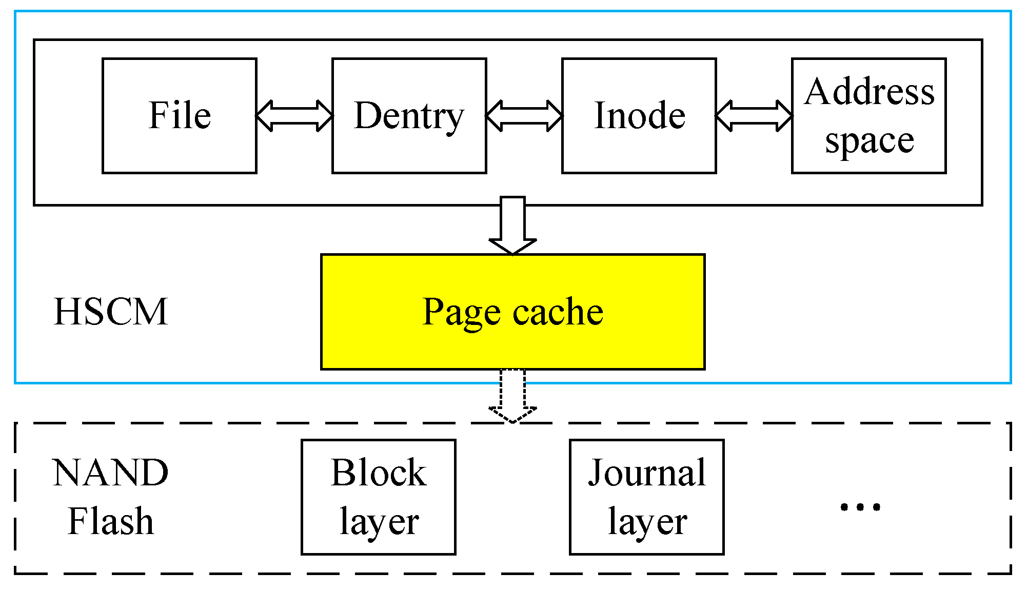
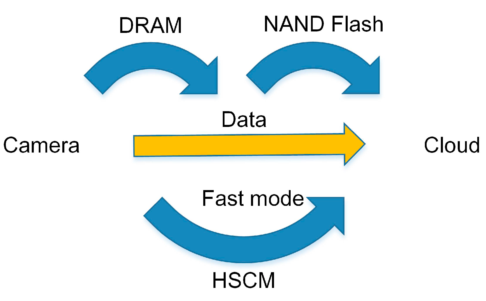
3. Fast Mode for HSCM with In-Memory File System

PCM is expected to provide higher density than DRAM and can offer larger capacity. In the traditional method, most data must eventually be stored in non-volatile storage, such as NAND Flash, which is usually slow. The HSCM helps to extend space for memory, and it is large enough for processing complicated applications, so the in-memory file system can be used to improve system performance. Existing non-volatile memory file systems, such as PMFS [25], NOVA [26], and SCMFS [27], are optimized for non-volatile memory. However, these non-volatile memory file systems use clflush and mfence of x86 for ordering guarantees, which could not be implemented in an ARM processor and other RISC processors for IoT devices. The persistence of the memory file system takes up many resources, and these non-volatile memory file systems are not fit for hybrid memory systems. For AIoT devices, improved performance is more valuable in some cases. Based on the advantages of HSCM, we can obtain a higher performance at the system level.
A fast mode for hybrid storage class memory is proposed. In IoT devices, since the proposed HSCM provides a large enough memory space, the conventional two-level memory system (DRAM and NAND Flash) can be replaced by one-level storage class memory (HSCM). Using an in-memory file system can reduce the number of data movements, and it is possible to implement calculations in memory [28]. tmpfs is an in-memory file system that is based on page cache. Fundamentally, tmpfs is not a file system focused on non-volatile memory. It was originally designed for DRAM-based main memory to provide rapid temporary storage space. There is no mechanism like journaling for persistency in tmpfs [29], but it is a better solution for non-volatile memory with better IO performance. Due to the large space and low power hybrid memory for tmpfs, this in-memory file system works well. Therefore, tmpfs is an optimal solution for the proposed design. We implemented the tmpfs-based, in-memory file system in the proposed HSCM architecture. By changing the way the file system managed, a large amount of intermediate data in applications of image processing can be put into HSCM. This method avoids the persistence overhead of the persistent file system. At the same time, it reduces the number of data exchange times between HSCM and external slow storage. The in-memory file system for HSCM is shown in Figure 7.
An AIoT device is usually used as an edge device in the system. This also means that there are not much data that need to be persistent in the device. In particular, applications of image processing in IoT devices usually need to process pictures or videos on-site, and only a small amount of the resulting data will be uploaded to the cloud. In this case, a large amount of data are processed in a short time, but most of the processed data will be discarded after processing. Therefore, only retaining a small NAND Flash as a persistent storage device can meet the requirements of IoT devices.

4. Evaluation

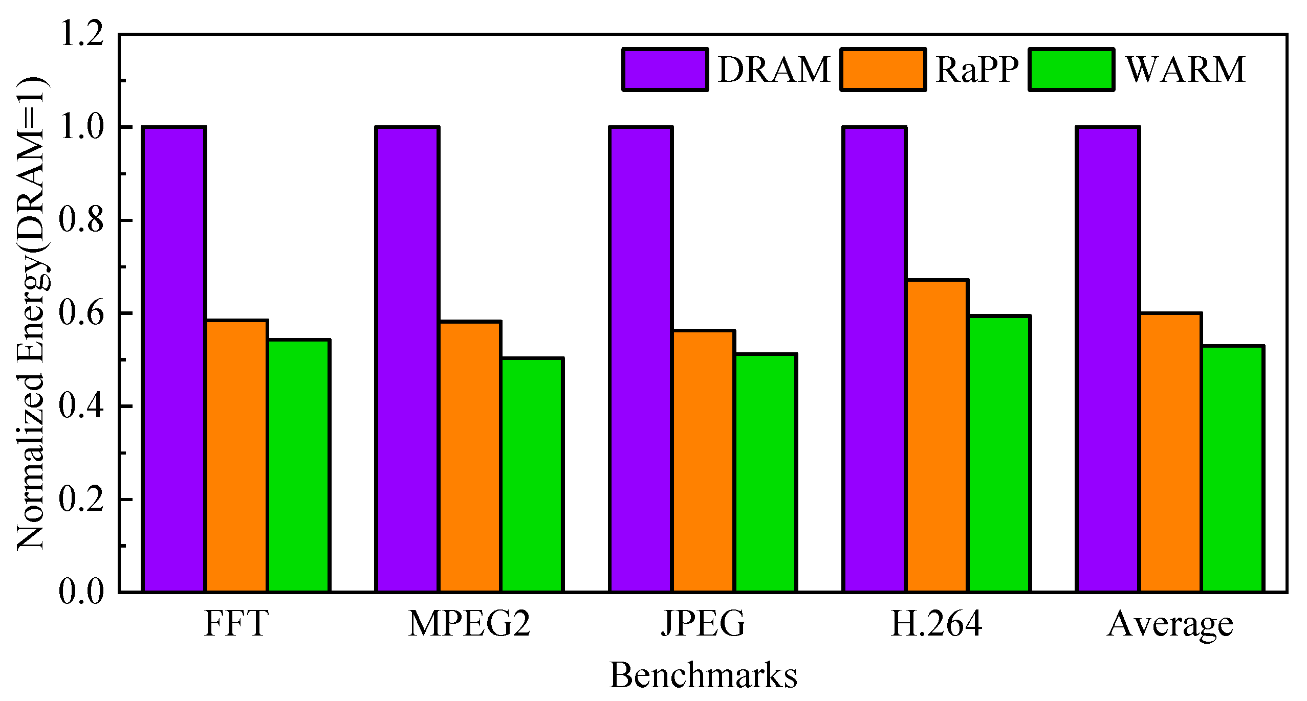
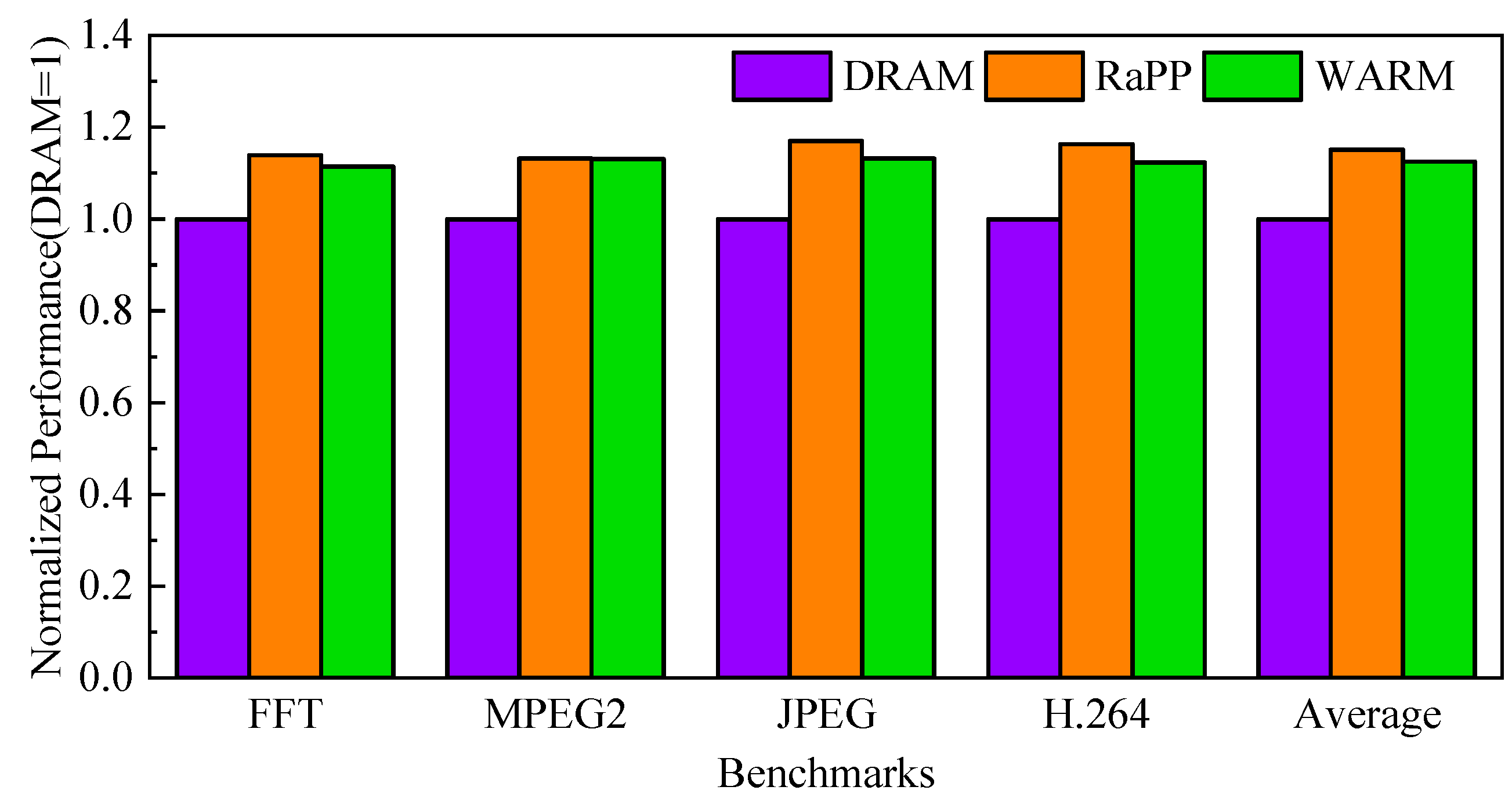
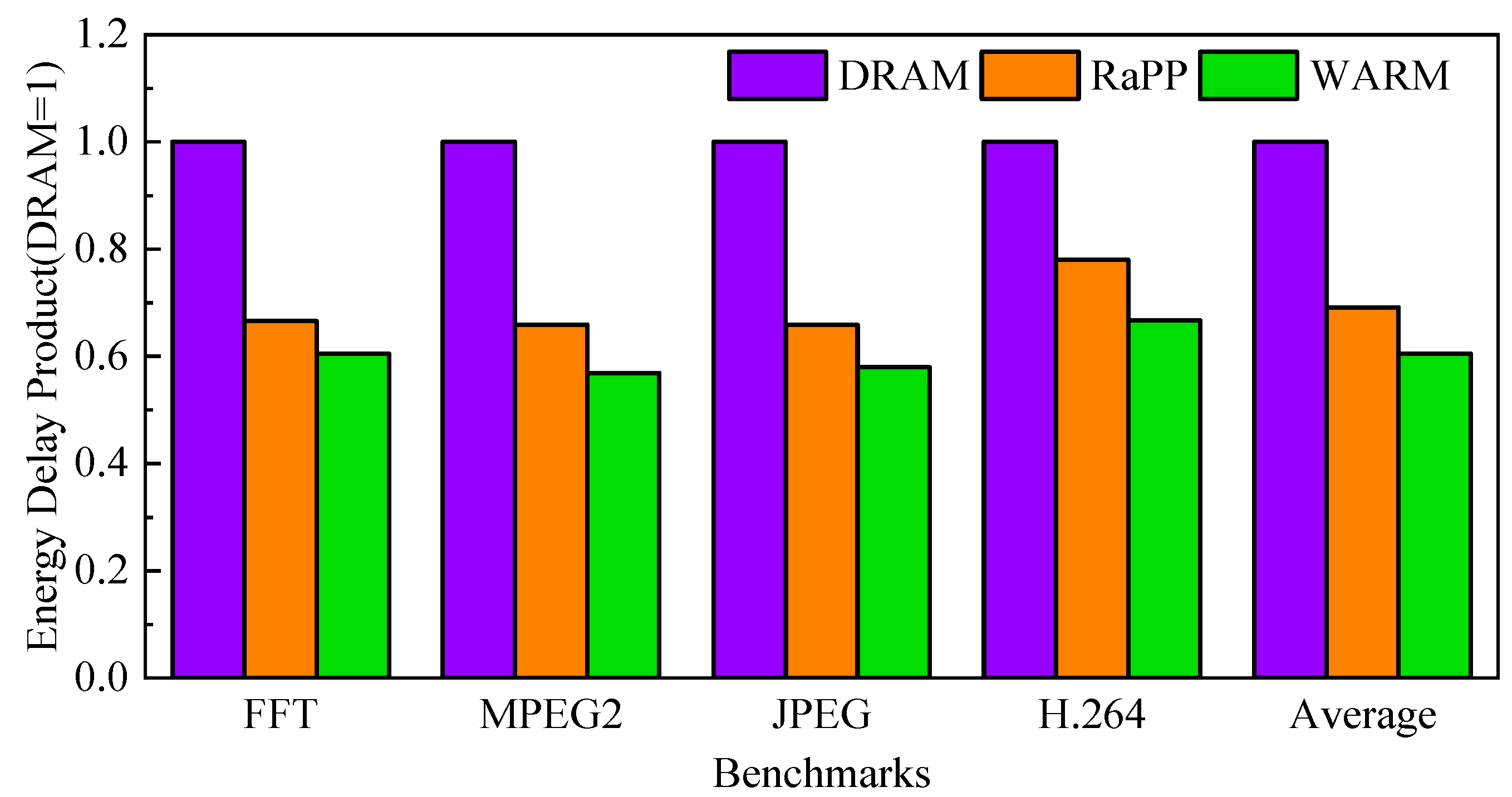
4.1. Evaluation of Hybrid Storage Class Memory

We evaluated the performance and energy efficiency of HSCM using the gem5 [23] and NVMain [30] simulators. The HSCM consists of a 1-GB DRAM and 3-GB PCM in a unified address space. The WARM counter and remap table were implemented in the memory controller. The memory controller migrates rows with more write operations and buffer misses from PCM to DRAM. Table 1 shows the relevant parameters.
The parameters of DRAM and PCM can be seen in Table 2 [24,31].
We ran benchmarks for 10 million instructions from Mibench [20] and MediaBench [21] using the simulators gem5 and NVMain. According to Section 2, the migration threshold can be set to one. When a row in PCM is accessed by a write operation or when a row buffer miss occurs, it will be migrated to DRAM. In general, the threshold and the weighing factors of a write and row buffer miss can be set to any value depending on the memory access patterns of the applications. These can be adjusted according to different applications to improve the algorithm. As the performance of PCM improves, this factor will also be adjusted.
From previous tests described in Section 2.2, we found that some IoT applications have a low memory footprint. The large capacity of HSCM could not be fully utilized. The applications of image processing have a higher pressure on memory and are widely deployed in AIoT terminals. To focus on a performance evaluation of image processing, we selected some applications from Mibench and MediaBench, including image processing (cjpeg and djpeg), video processing (h264dec, h264enc, mpeg2dec, and mpeg2enc) and signal processing (FFT). The results of normalized energy consumption are illustrated in Figure 8.
As can be seen in Figure 8, DRAM represents the case where a 4-GB DRAM-only main memory is implemented in the system. RaPP represents a hybrid main memory consisting of a 1-GB DRAM and 3-GB PCM with a hardware-based method [18]. WARM shows the energy of our proposed method. To compare the energy consumption and performance between the advanced hardware-based scheme, RaPP, and the proposed scheme, WARM, both were implemented in a memory controller with the same hybrid main memory structure in the system. The results indicate that the energy of the HSCM architecture is lower than that of DRAM. In the composition of energy consumption, the dynamic energy (such as read and write energy) is only part of it. The refresh mechanism of DRAM induces energy consumption even when no activity occurs in the memory, and this refresh mechanism is not needed in PCM because it is non-volatile. Although the PCM’s write energy is higher than DRAM, the static energy consumption is much lower than DRAM. By applying our WARM scheme, the rows with frequent write operations and row buffer misses are migrated from PCM to DRAM. This effectively reduces the precharge operation in PCM, thereby further reducing the energy consumption of the memory system. For energy-constrained IoT devices, the reduction of energy consumption is of great significance. However, the HSCM also causes a decrease in the latency of the memory system. The results of normalized performance are shown in Figure 9.
As can be seen in Figure 9, the decline in system performance is unavoidable because of the high write latency in PCM. We can only reduce the performance loss as much as possible through algorithms. Compared to a DRAM-only situation, the RaPP scheme consumes up to 43.8% less energy (on average, 40.1%), with a performance overhead of less than 15.1%. Our proposed scheme consumes up to 49.7% less energy (on average, 46.2%) with a performance overhead of less than 12.5%. This is because the WARM scheme considers the influence of the row buffer miss. Furthermore, the WARM scheme removes the redundant queue upgrade process and selects the rows that need to be migrated quickly. In order to prevent redundant migration, complex upgrade and downgrade strategies are implemented in RaPP, which are not designed to solve the problems for IoT applications. The memory access patterns in IoT applications are different. Thus, the proposed scheme is more effective than RaPP.
To consider energy consumption and performance comprehensively, we use the energy delay product parameter to evaluate the effect of different strategies. As can be seen in Figure 10, the energy delay product of RaPP and WARM is reduced by 31.9% and 39.5%, compared with DRAM, respectively. From the perspective of energy delay product, the WARM scheme has more advantages. This shows that the HSCM system has practical value. It is worth noting that the IoT devices are usually in a standby state. The above test is mainly for the complex tasks with a large memory footprint. If it stays on standby for a long time, since the PCM does not need to be refreshed, this will make the energy consumption advantage of the memory system more pronounced. Moreover, for applications with less memory pressure, the advantages of the HSCM with the proposed scheme are more significant.
As mentioned above, we set the initial ratio of DRAM and PCM as 1:3. This is a common configuration for hybrid memory. We tested the impact of different ratios on energy consumption and performance. When the proportion of DRAM increases, the energy consumption obviously increases. At the same time, the performance will be improved because the latency of DRAM is lower than that of PCM. In contrast, when the proportion of PCM increases, the energy consumption decreases because less DRAM needs to be refreshed. However, the above effects were relatively minor in our test. The initial ratio of DRAM and PCM is a more suitable ratio and is more like the actual size of a commercial product.
Additionally, the WARM scheme has a lower hardware cost than RaPP. Compared with the RAPP strategy, the proposed scheme has a simpler hardware structure. The total additional storage implemented in the memory controller in our design is 20 kB, including 16 kB for the remap table and 4 kB for the WARM counter, which is enough to implement the current algorithm. As shown in Figure 4, a few rows need to be migrated in the applications of image processing. Consequently, there is no need for the memory controller to maintain a large table to record the message for each row. In addition, because of the limited storage resource in the memory controller, when the remap table is full, it will be reset. This has a negligible impact on the applications of image processing.

4.2. Performance of the Fast Mode

Even though the WARM scheme reduces energy consumption, it leads to performance degradation because of the high latency in PCM. In comparison with the high performance of DRAM, the HSCM still has certain deficiencies. In order to make full use of the large capacity of HSCM, some processes, which should be handled in storage such as NAND Flash, can be placed in HSCM instead. This fast mode speeds up certain applications in AIoT devices.
By using the proposed fast mode with a tmpfs-based file system, the performance of the IoT system can be improved. For instance, in video processing devices, the analog video signals produced by the video camera are converted into digital signals. They are then converted into video files by the H.264 encoder and stored in the NAND Flash because DRAM space is limited and much more expensive. In the fast mode, the HSCM provides enough space for video processing. Furthermore, the video files can be processed and stored in HSCM temporarily. Some valuable files are delivered to other programs for further processing. Nowadays, IoT devices are able to perform complex computations and a variety of tasks on-site. These processed video files or results can be directly uploaded to the cloud from HSCM. Compared with the conventional DRAM and NAND Flash architecture, the HSCM with fast mode saves energy in video processing and reduces the IO times. In addition, the traditional mode and the fast mode can coexist. Different modes can adapt to different requirements. The difference between the two modes is illustrated in Figure 11.
To verify the performance of the tmpfs-based, in-memory file system, we used the ALTERA HAN Pilot Platform with an ARM Cotex-A9 processor for the test. Since there is no commercial PCM product, we still use the DRAM memory in our test. The 1-GB DRAM on the platform was used to simulate hybrid storage class memory. In fact, the performance of the HSCM architecture is close to DRAM as shown in Section 4.1. We used the results measured by DRAM, and corrected the results according to the performance ratio of PCM and DRAM. To make the results more convincing, we used poor PCM read and write performance parameters and the DRAM parameters at the system level from reference [32]. Therefore, the IOPS value of the fast mode finally displayed is worse than the actual measured value by using the DRAM. In the test, we used the FIO benchmark to test the performance of sequential read, sequential write, random read, and random write, respectively.
We evaluated the IOPS (input/output operations per second) in different IO size between the conventional file system based on block device and the in-memory file system based on HSCM. In particular, considering the loss of PCM’s read and write performance at the system level, we revised the results based on the parameters provided in [32]. The following table lists the IOPS ratio of the HSCM with tmpfs and the conventional architecture (DRAM and NAND Flash) with ext3. The results of the ratio in different IO sizes are shown in Table 3.
As can be seen in the Table 3, the HSCM architecture with the tmpfs-based, in-memory file system is a proper method to improve system IO performance. The proposed method has more than 30 times the IOPS than the conventional architecture on average. We used the PCM delay parameters in the system level to revise the ratio value of IOPS. Since the conventional file systems are equipped with reliability techniques such as journaling, when the redundant block layer and journal layer are removed, files can be maintained in the page cache in HSCM.
In conclusion, HSCM provides a larger memory space that can improve the processing ability of IoT devices. By completing most of the image processing in HSCM, the swaps of data between the main memory (HSCM) and the slow storage (NAND Flash) are effectively reduced. As the capacity of HSCM becomes larger, the capacity of NAND Flash can become smaller. In fact, HSCM partially replaces NAND Flash. In this paper, the fast mode cannot exist without the conventional file system. The NAND Flash still exists and plays an important role. We will continue to study the persistence of HSCM. The NAND Flash will be completely replaced by HSCM without significantly affecting the performance of the system.

5. Conclusions

In this paper, we propose an HSCM architecture managed by the row buffer locality and the write aware scheme. A fast mode with the tmpfs-based, in-memory file system was implemented to improve the IO performance of the system. The proposed architecture can reduce the energy consumption of an IoT device by up to 49.7% and increase the IO performance by more than 30 times for certain applications on average. The proposed hybrid storage class memory system can meet the requirements of low power and high performance for AIoT devices. A non-volatile memory device gives rise to many challenges and more opportunities. With the development of non-volatile storage technologies such as PCM, hybrid storage class memory will become a trend in the future.

Author Contributions

Conceptualization, H.S. and L.C.; methodology, H.S.; validation, H.S., C.L. and M.N.; formal analysis, H.S. and X.H.; investigation, H.S.; resources, L.C.; data curation, H.S.; writing—original draft preparation, H.S.; writing—review and editing, X.H. and L.C.; visualization, H.S.; supervision, L.C.; project administration, L.C.; funding acquisition, L.C. All authors have read and agreed to the published version of the manuscript.

Funding

This research was funded by the National Key R&D Program of China under Grant 2019YFB2102400.

Acknowledgments

The authors would like to thank anonymous reviewers for their special effort.

Conflicts of Interest

The authors declare no conflict of interest.

References

  1. Samie, F.; Bauer, L.; Henkel, J. IoT technologies for embedded computing: A survey. In Proceedings of the Eleventh IEEE/ACM/IFIP International Conference on Hardware/Software Codesign and System Synthesis—CODES ’16, Pittsburgh, PA, USA, 2–7 October 2016; pp. 1–10. [Google Scholar]
  2. Hassan, N.; Gillani, S.; Ahmed, E.; Yaqoob, I.; Imran, M. The Role of Edge Computing in Internet of Things. IEEE Commun. Mag. 2018, 56, 110–115. [Google Scholar] [CrossRef]
  3. Song, W.; Zhou, Y.; Zhao, M.; Ju, L.; Xue, C.J.; Jia, Z. EMC: Energy-Aware Morphable Cache Design for Non-Volatile Processors. IEEE Trans. Comput. 2019, 68, 498–509. [Google Scholar] [CrossRef]
  4. Yun, J.-T.; Yoon, S.-K.; Kim, J.-G.; Burgstaller, B.; Kim, S.-D. Regression Prefetcher with Preprocessing for DRAM-PCM Hybrid Main Memory. IEEE Comput. Arch. Lett. 2018, 17, 163–166. [Google Scholar] [CrossRef]
  5. Wong, H.-S.P.; Raoux, S.; Kim, S.; Liang, J.; Reifenberg, J.P.; Rajendran, B.; Asheghi, M.; Goodson, K.E. Phase Change Memory. Proc. IEEE 2010, 98, 2201–2227. [Google Scholar] [CrossRef]
  6. Kim, N.S.; Song, C.; Cho, W.Y.; Huang, J.; Jung, M. LL-PCM: Low-Latency Phase Change Memory Architecture. In Proceedings of the 56th Annual Design Automation Conference 2019, Las Vegas, NV, USA, 2–6 June 2019; pp. 1–6. [Google Scholar]
  7. Apalkov, D.; Ong, A.; Driskill-Smith, A.; Krounbi, M.; Khvalkovskiy, A.; Watts, S.; Nikitin, V.; Tang, X.; Lottis, D.; Moon, K.; et al. Spin-transfer torque magnetic random access memory (STT-MRAM). J. Emerg. Technol. Comput. Syst. 2013, 9, 1–35. [Google Scholar] [CrossRef]
  8. Akinaga, H.; Shima, H. Resistive Random Access Memory (ReRAM) Based on Metal Oxides. Proc. IEEE 2010, 98, 2237–2251. [Google Scholar] [CrossRef]
  9. Foong, A.; Hady, F. Storage As Fast As Rest of the System. In Proceedings of the 2016 IEEE 8th International Memory Workshop (IMW), Paris, France, 15–18 May 2016; pp. 1–4. [Google Scholar]
  10. Boukhobza, J.; Rubini, S.; Chen, R.; Shao, Z. Emerging NVM: A survey on architectural integration and research challenges. ACM Trans. Des. Autom. Electron. Syst. 2017, 23, 1–32. [Google Scholar] [CrossRef]
  11. Asadinia, M.; Bobda, C. Enhancing Lifetime of PCM-Based Main Memory with Efficient Recovery of Stuck-at Faults. In Proceedings of the 2018 IEEE Computer Society Annual Symposium on VLSI (ISVLSI), Hong Kong, China, 8–11 July 2018; pp. 357–362. [Google Scholar]
  12. Zilberberg, O.; Weiss, S.; Toledo, S. Phase-change memory: An architectural perspective. ACM Comput. Surv. 2013, 45, 1–33. [Google Scholar] [CrossRef]
  13. Chen, X.; Sha, E.H.-M.; Jiang, W.; Zhuge, Q.; Chen, J.; Qin, J.; Zeng, Y. The design of an efficient swap mechanism for hybrid DRAM-NVM systems. In Proceedings of the 13th International Conference on Embedded Software—EMSOFT ’16, Pittsburgh, PA, USA, 2–7 October 2016; pp. 1–10. [Google Scholar]
  14. Salkhordeh, R.; Asadi, H. An Operating System Level Data Migration Scheme in Hybrid DRAM-NVM Memory Architecture. In Proceedings of the 2016 Design, Automation & Test in Europe Conference & Exhibition (DATE), Dresden, Germany, 14–18 March 2016; pp. 936–941. [Google Scholar]
  15. Liu, D.; Zhong, K.; Zhu, X.; Li, Y.; Long, L.; Shao, Z. Non-Volatile Memory Based Page Swapping for Building High-Performance Mobile Devices. IEEE Trans. Comput. 2017, 66, 1918–1931. [Google Scholar] [CrossRef]
  16. Bock, S.; Childers, B.R.; Melhem, R.; Mosse, D. Concurrent Migration of Multiple Pages in software-managed hybrid main memory. In Proceedings of the 2016 IEEE 34th International Conference on Computer Design (ICCD), Scottsdale, AZ, USA, 2–5 October 2016; pp. 420–423. [Google Scholar]
  17. Jia, G.; Han, G.; Xie, H.; Du, J. Hybrid-LRU Caching for Optimizing Data Storage and Retrieval in Edge Computing-Based Wearable Sensors. IEEE Internet Things J. 2019, 6, 1342–1351. [Google Scholar] [CrossRef]
  18. Ramos, L.E.; Gorbatov, E.; Bianchini, R. Page placement in hybrid memory systems. In Proceedings of the ICS ’11: International Conference on Supercomputing, Tucson, AZ, USA, 1–4 June 2011; pp. 85–95. [Google Scholar]
  19. Alawneh, T.A. A Dynamic Row-Buffer Management Policy for Multimedia Applications. In Proceedings of the 2019 27th Euromicro International Conference on Parallel, Distributed and Network-Based Processing (PDP), Pavia, Italy, 13–15 February 2019; pp. 148–157. [Google Scholar]
  20. Guthaus, M.R.; Ringenberg, J.S.; Ernst, D.; Austin, T.M.; Mudge, T.; Brown, R.B. MiBench: A free, commercially representative embedded benchmark suite. In Proceedings of the Fourth Annual IEEE International Workshop on Workload Characterization, WWC-4 (Cat. No.01EX538), Austin, TX, USA, 2 December 2001; pp. 3–14. [Google Scholar]
  21. Fritts, J.E.; Steiling, F.W.; Tucek, J.A.; Wolf, W. MediaBench II Video: Expediting the next generation of video systems research. Microprocess. Microsyst. 2009, 33, 301–318. [Google Scholar] [CrossRef] [Green Version]
  22. Wang, Q.; Chen, L.; Hao, X. Hybrid memory system using memory access-aware remapping mechanism. J. Chin. Comput. Syst. 2014, 6, 1201–1206. [Google Scholar]
  23. Binkert, N.; Sardashti, S.; Sen, R.; Sewell, K.; Shoaib, M.; Vaish, N.; Hill, M.D.; Wood, D.A.; Beckmann, B.; Black, G.; et al. The gem5 simulator. ACM SIGARCH Comput. Archit. News. 2011, 39, 1–7. [Google Scholar] [CrossRef]
  24. Li, Y.; Ghose, S.; Choi, J.; Sun, J.; Wang, H.; Mutlu, O. Utility-Based Hybrid Memory Management. In Proceedings of the 2017 IEEE International Conference on Cluster Computing (CLUSTER), Honolulu, HI, USA, 5–8 September 2017; pp. 152–165. [Google Scholar]
  25. Dulloor, S.R.; Kumar, S.; Keshavamurthy, A.; Lantz, P.; Reddy, D.; Sankaran, R.; Jackson, J. System software for persistent memory. In Proceedings of the Ninth European Conference on Computer Systems—EuroSys ’14, Amsterdam, The Netherlands, 14–16 April 2014; pp. 1–15. [Google Scholar]
  26. Xu, J.; Swanson, S. NOVA: A Log-structured File System for Hybrid Volatile/Non-volatile Main Memories. In Proceedings of the FAST’16: Proceedings of the 14th Usenix Conference on File and Storage Technologies, Santa Clara, CA, USA, 22–25 February 2016; pp. 323–338. [Google Scholar]
  27. Wu, X.; Qiu, S.; Narasimha Reddy, A.L. SCMFS: A File System for Storage Class Memory and its Extensions. ACM Trans. Storage 2013, 9, 1–23. [Google Scholar] [CrossRef]
  28. Siegl, P.; Buchty, R.; Berekovic, M. Data-Centric Computing Frontiers: A Survey On Processing-In-Memory. In Proceedings of the Second International Symposium on Memory Systems - MEMSYS ’16, Alexandria, VA, USA, 3–6 October 2016; pp. 295–308. [Google Scholar]
  29. Kim, H.; Ahn, J.; Ryu, S. In-Memory File System for Non-Volatile Memory. In Proceedings of the RACS ’13: Proceedings of the 2013 Research in Adaptive and Convergent Systems, Montreal, QC, Canada, 1–4 October 2013; pp. 479–484. [Google Scholar]
  30. Poremba, M.; Zhang, T.; Xie, Y. NVMain 2.0: A User-Friendly Memory Simulator to Model (Non-)Volatile Memory Systems. IEEE Comput. Arch. Lett. 2015, 14, 140–143. [Google Scholar] [CrossRef]
  31. Liu, H.; Chen, Y.; Liao, X.; Jin, H.; He, B.; Zheng, L.; Guo, R. Hardware/software cooperative caching for hybrid DRAM/NVM memory architectures. In Proceedings of the International Conference on Supercomputing—ICS ’17, Chicago, IL, USA, 14–16 June 2017; pp. 1–10. [Google Scholar]
  32. Salkhordeh, R.; Mutlu, O.; Asadi, H. An Analytical Model for Performance and Lifetime Estimation of Hybrid DRAM-NVM Main Memories. IEEE Trans. Comput. 2019, 68, 1114–1130. [Google Scholar] [CrossRef] [Green Version]
Figure 1. Hybrid storage class memory architecture.
Electronics 09 01013 g001
Figure 2. Row buffer architecture with an open page strategy.
Electronics 09 01013 g002
Figure 3. Spatial locality of IoT applications.
Electronics 09 01013 g003
Figure 4. Concentration of write operations.
Electronics 09 01013 g004
Figure 5. Memory controller architecture.
Electronics 09 01013 g005
Figure 6. WARM counter.
Electronics 09 01013 g006
Figure 7. File system for HSCM.
Electronics 09 01013 g007
Figure 8. Normalized energy.
Electronics 09 01013 g008
Figure 9. Normalized performance.
Electronics 09 01013 g009
Figure 10. Energy delay product.
Electronics 09 01013 g010
Figure 11. Video applications in IoT devices.
Electronics 09 01013 g011
Table 1. System configuration.
ParameterValue
CPU
Frequency
ARM (1 core)
1 GHz
L1 cache32 kB instruction cache
32 kB data cache
L2 cache512 kB
Memory1-GB DRAM
3-GB PCM
Table 2. DRAM and PCM parameters.
DRAMPCM
LatencytCL = 15 ns
tRCD = 15 ns
tCWD = 13 ns
tWR = 15 ns
tCL = 15 ns
tRCD = 48 ns
tCWD = 13 ns
tWR = 300 ns
EnergyArray read = 1.17 pJ/bit
Array write = 0.39 pJ/bit
Row buffer read = 0.93 pJ/bit
Row buffer write = 1.02 pJ/bit
Array read = 2.47 pJ/bit
Array write = 16.82 pJ/bit
Row buffer read = 0.93 pJ/bit
Row buffer write = 1.02 pJ/bit
Table 3. The IOPS of proposed file system.
IO Size1 kB2 kB4 kB8 kB16 kBAverage
Ratio38.7454.6219.3114.6423.0230.07

