Article

Novel Low-Cost Power Divider for 5.8 GHz

International College of Semiconductor Technology, National Chiao Tung University, Hsinchu 30010, Taiwan
*
Author to whom correspondence should be addressed.
Electronics 2020, 9(4), 699; https://doi.org/10.3390/electronics9040699
Submission received: 30 March 2020 / Revised: 19 April 2020 / Accepted: 23 April 2020 / Published: 24 April 2020
(This article belongs to the Section Microwave and Wireless Communications)

Abstract

:
This paper presents a new capacitive lump-free structure for power dividers using a printed-circuit board, while maintaining size reduction and physical isolation. The conventional lumped capacitors approach has self-resonant problem and cause worse S 22 and isolation at high frequencies. To overcome such technical issues, the coupled-line structures were introduced in the isolation network. After optimizing the distance between output ports and position of the isolation network, tuning the characteristic impedance and electrical length of transmission lines can decide the value of the lump resistor. The first example was designed at 1 GHz, and the resistor in the isolation network was 330 ohm, having 0.2-dB insertion loss and 19% total bandwidth, while maintaining 80-degree distance between split ports and 180-degree total length, providing 21% to 67% size reduction. The second example was designed at 5.8 GHz, which was five times greater than in past research, using an RO4003C substrate while maintaining a 0.24-dB insertion loss, 17% total bandwidth, and 0.06 dB amplitude imbalance, which was only 0.01 dB more than in recent research. Such superior performance is mainly attributed to the coupled transmission lines in the isolation network featuring a capacitive lump-free isolation network. Our data indicate that amplitude imbalance, bandwidth, and miniaturization are superior to any published data.

1. Introduction

The Wilkinson power divider (WPD) [1] is one of the most commonly used passive components in transmitter subsystems. A conventional WPD has two quarter-wavelength transmission lines with high impedance with a resistor as the isolation network (INW). To reduce the physical size of the conventional WPD, capacitive loading was applied to the high impedance lines [2]. Through the external loading of the capacitors, the electrical length at the center frequency can be maintained with a shorter physical length. While such an approach seems straightforward, the reduction in size usually leads to the very short physical separation between the output ports. This may become a serious issue for phased-array applications since the existence of unwanted but unavoidable coupling between antenna elements certainly deteriorates the system performance.
Complex isolation networks were widely adopted to address the issue of achieving physical isolation while maintaining electrical isolation [3]. In addition to the resistor, reactive components, mainly capacitors, were included in the INW. Meanwhile, the position of the INW must be optimized such that the impedance matching conditions can be satisfied at the desired frequency bands of operation. Successful implementation of such a concept can be found in [3,4,5,6,7,8] with extension to the general N-way power dividers [4,5,6]. While the efforts were mainly devoted to keeping the overall electrical length to be the same as the conventional WPD (180 degrees), further reduction in the transmission-line length was possible by replacing the high-impedance section with coupled lines [7].
Practically, adoption of the lumped capacitors in the complex INW may have problem when the operating frequency is close to or beyond the self-resonant frequency of the capacitor, which deteriorates output return loss and isolation. Poor output return loss and isolation cause the phased array to have the signal reflected at the output connected to the power amplifier. Several attempts utilized resistor-only INW for high-frequency operations up to millimeter-wave frequencies with extended arms [9,10,11,12,13]. Despite the good performance achieved, such an approach always has the disadvantage of being bulky in size, which makes it applicable only in a regime where the operating wavelength is short.
Apparently, for practical implementation scenarios in the popular microwave frequency range at S- and C-bands, a new configuration is necessary for power dividers to feature size minimization with port extension. Most importantly, removal of the lumped capacitor in the complex INW is necessary, since the self-resonance of the surface-mount-device (SMD) capacitors usually occurs around the band of interest. In this paper, we propose a new configuration for power divider targeting for C-band operation featuring size minimization with port extension. A coupled-line section with an open end was introduced in the complex INW to replace the lumped capacitor. The design sequence with the synthesis procedure is demonstrated based on the even- and odd-mode analysis theoretically. Experimental implementation using standard printed-circuit-board (PCB) technology, one at 1 GHz and the other at 5.8 GHz, was performed to validate the theoretical derivation. Measurement results were in good agreement with simulation ones, exhibiting good overall performance in terms of return loss, isolation, and amplitude imbalance over a relatively wide bandwidth with a substantial size reduction compared to previous publications.

2. Design and Analysis

Figure 1 shows the configuration of the proposed power divider with a coupled-line section adopted in the complex isolation network. Due to the symmetric nature of the geometry, analysis of such configuration is generally performed by placing either an open-circuited or short-circuited bisecting plane at the plane of symmetry.

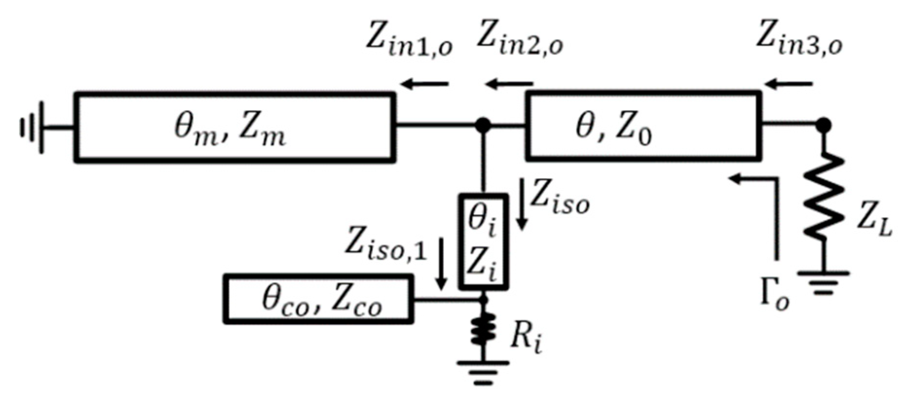
2.1. Even-Mode Analysis

Figure 2 shows the even-mode subnetwork when an open-circuit bisection is applied on the plane of symmetry centered between the coupled-line sections in the isolation network.
With the source and load terminated by the source impedance ZS and load impedance ZL, respectively, the impedance Z0 of the main arms connecting the common port and split ones satisfies the conventional relation of a regular Wilkinson power divider as Z 0 = 2 Z L Z S . In our configuration, with the location of the INW moved closer to the common port for the purpose of physical isolation, choice of high impedance line with impedance Zm and extra loading for size reduction is possible. The impedance at the location of INW looking into the common port, Zin2,e, can be derived as
Z i n 2 , e = Z m Z i n 1 , e + j Z m t a n θ m Z m + j Z i n 1 , e t a n θ m ,  
where
Z i n 1 , e = ( 1 2 Z S + j B i ) 1
The input impedance of the isolation network in the even-mode subnetwork is
Z i n 3 , e = j Z i Z i t a n θ i t a n θ c e Z c e Z i t a n θ c e + Z c e t a n θ i ,
In the above equation, Z i and θ i are the characteristic impedance and electrical length of transmission lines connecting with the coupled transmission lines in the isolation network, respectively. Z c e and θ c e are the even-mode characteristic impedance and electrical length of the coupled-line section, respectively. The reflection coefficient at the split port can then be readily expressed as
Γ e = Z i n 5 , e Z L Z i n 5 , e + Z L ,
where
Z i n 5 , e = Z 0 Z i n 4 , e + j Z 0 t a n θ Z 0 + j Z i n 4 , e t a n θ ;
and
Z i n 4 , e = ( 1 Z i n 2 , e + 1 Z i n 3 , e ) 1 .
For minimizing the output reflection at the split port, we set Γ e = 0 , which leads to the synthesis of the remaining parameters as
θ m = sin 1 ( Z 0 Z m cos θ ) ,
B i = cos θ m sin θ Z 0 cos θ ,
Z ce = tan θ ce Z i 2 tan θ i ( sin θ cos θ m ) Z o Z i cos θ Z i ( sin θ cos θ m ) + Z o cos θ tan θ i .
In the above equations, once the location of the complex INW ( θ , which is less than 90 degrees) is determined, the choice of Zm determines the electrical length θ m . In general, a higher Zm is preferable for the purpose of compactness. The extra loading susceptance ( B i ) for further reduction in the electrical length is then uniquely determined by the relationship in Equation (8).

2.2. Odd-Mode Analysis

For the odd-mode analysis, a short-circuit bisecting plane instead was placed at the plane of symmetry. Figure 3 shows the odd-mode subnetwork after bisection.
The corresponding derivation and analysis procedure is mainly the same as the even-mode case with the following impedance relations:
Z i n 1 , o = j Z m tan θ m ,
Z i s o , 1 = ( 1 R i + j tan θ c o Z c o ) 1 ,
Z i s o = Z i Z i s o , 1 + j Z i tan θ i Z i + j Z i s o , 1 tan θ i ,
where Zco and θco are the impedance and electrical length of the coupled-line section at odd-mode, respectively. Ri is the corresponding resistance in the complex INW. The reflection coefficient at the split port under odd-mode excitation can be calculated as
Γ o = Z i n 3 , o Z L Z i n 3 , o + Z L ,
with
Z i n 3 , o = Z o Z i n 2 , o + j Z o tan θ Z o + j Z i n 2 , o tan θ ,
and
Z i n 2 , o = ( 1 Z i n 1 , o + 1 Z i s o ) 1 .
Setting the matched condition at the output port, Γ o = 0 , leads to
Z c o = tan θ c o ( Z i + B 1 Z i 2 tan θ i ) 2 + ( G 1 Z i 2 tan θ i ) 2 ( Z i + B 1 Z i 2 tan θ i ) ( Z i B 1 tan θ i ) + Z i 3 G 1 2 tan θ i ,
where the G 1 and B 1 are
G 1 = ( 1 + tan 2 θ ) Z L Z L 2 + Z o 2 tan 2 θ ,
B 1 = 1 Z m t a n θ m + Z o 2 Z L 2 Z o ( Z L 2 + Z o 2 tan 2 θ ) tan θ .
Finally, the resistance Ri of the complex INW can be readily synthesized as
R i = ( Z i + B 1 Z i 2 tan θ i ) 2 + ( G 1 Z i 2 tan θ i ) 2 Z i G 1 [ ( Z i + B 1 Z i 2 tan θ i ) Z i tan θ i ( Z i B 1 tan θ i ) ] .
Based on the previous derivations, once the location of the complex INW (θ) is determined, analytical solutions of the remaining parameters are uniquely defined with the proper choice of the even- and odd-mode characteristic impedance of the coupled-line section. The choice of the corresponding impedance at even- and odd-mode determines the coupling factor as
K = 20 log ( Z c e Z c o Z c e + Z c o ) ,
which is an indicator of the physical separation between the two transmission lines for the real implementation scenario. Practically, due to the limit of fabrication tolerance, the value of K should fall in some reasonable range. For example, the magnitude of K ( | K | ) for Rogers RO4003C PCB with 0.508 mm thickness has to be greater than 4 dB since the minimum gap between the transmission lines is limited to 50 μm for the standard fabrication process. In general, higher levels of Zce and Zco lead to shorter physical length of the coupled line. Figure 4 shows the complete design procedure for the proposed configuration.

3. Experimental Verification

In order to validate the theoretical analysis of the proposed configuration, two prototypes, one centered at 1 GHz and the other at 5.8 GHz, were designed, fabricated, and characterized. For both designs, we started with the selection of the location of complex INW at θ = 20° In order to have substantial reduction in the overall sizes, the impedance Zm was chosen to be 120 Ω, leading to the electrical length θm of 33.6 degrees. Figure 5 shows the layout of the synthesized power divider with definitions of the physical geometries. The designs were implemented on RO4003C PCB substrate with a dielectric constant of 3.38, thickness of 0.508 mm, and loss tangent of 0.0028. The detailed dimensions for both designs are listed in Table 1 with all the units in μm.
Figure 6a shows the photo of the fabricated prototype designed at 1 GHz. The power divider was measured using an Anritsu MS46522A vector network analyzer. The measured and simulated return loss at the three ports are shown in Figure 6b. It can be observed that the fabricated prototype exhibited an impedance bandwidth (less than a 20-dB return loss) of 370 MHz, 386 MHz, and 246 MHz at ports 1, 2, and 3, respectively. Figure 6c shows the measured and simulated insertion loss and isolation. The insertion losses were measured to be 3.13 and 3.2 dB at port 2 and port 3, respectively, showing an additional loss other than the equal power splitting of 0.2 dB. Moreover, the isolation bandwidth for S 23 < −20 dB was measured to be 194 MHz and that for S 23   < −30 dB was measured to be 64 MHz. The characteristics of phase and amplitude imbalance are included in Figure 6d, showing only 1.14 degrees in phase and 0.07 dB in amplitude at 1 GHz, respectively. In all the cases, the measurement results agreed well with the simulation.
Figure 7a shows the photo of the fabricated prototype designed at 5.8 GHz. The power divider was measured using an Anritsu MS46522A vector network analyzer. For both prototypes, the 165 Ω resistor was adopted in the complex INW. The measured and simulated return loss at the three ports are shown in Figure 7b. It was observed that the fabricated prototype exhibited an impedance bandwidth (less than a 20-dB return loss) of 2.24 GHz, 2.28 GHz, and 0.978 GHz at ports 1, 2, and 3, respectively. Figure 7c shows the measured and simulated insertion loss and isolation. The insertion losses were measured to be 3.17 and 3.23 dB at port 2 and port 3, respectively, showing an additional loss other than the equal power splitting of 0.23 dB. Moreover, the isolation bandwidth for S 23   < −20 dB was measured to be 1.35 GHz and that for S 23   < −30 dB was measured to be 337 MHz. The characteristics of phase and amplitude imbalance are included in Figure 7d, showing only 1.2 degrees in phase and 0.06 dB in amplitude at 5.8 GHz, respectively. In all the cases, the measurement results agreed well with the simulation.
The performance comparison was made against previously published works [7,8,10,12,13] and are listed in Table 2, where the bandwidth ratio in percent was defined as the corresponding S-parameter, being less than −20 dB. While the impedance bandwidth at the common port of [7] outperformed the fabricated prototype, both the insertion loss and isolation bandwidth were narrower, leading to a limited practical bandwidth of operation. As for our case, the minimum practical bandwidth ratio of operation for the two prototypes was measured to be 19% and 17%, respectively. Comparing with a conventional Wilkinson power divider [2], this work acquired physical isolation and better bandwidth but with similar total length. In all, the measured performance of the two fabricated prototypes validated the theoretical analysis and the design procedure of the proposed configuration. Substantial size reduction with nice characteristics in terms of impedance bandwidth and isolation were demonstrated using only one lumped resistor in the complex INW as compared to previous publications. Such a superior performance difference was attributed to the replacement of the conventional capacitors using coupled-line structures in the isolation network, which satisfies the need for compact structure and complex isolation.

4. Conclusions

In this paper, we proposed a new configuration for the realization of a power divider featuring size compactness with port extension for suppression of coupling. Measured responses of the fabricated first prototype and second prototype exhibited practical operation bandwidths of 194 MHz centered at 1 GHz and 978 MHz centered at 5.8 GHz, respectively. Two prototypes achieved 26% to 67% size reduction and five times more operation frequency than past research with low amplitude imbalance. Such superior performance was mainly attributed to the utilization of the coupled-line structures in the complex isolation network to replace the capacitors in the conventional realization.

Author Contributions

Author Contributions: Conceptualization and methodology, H.-T.H. and T.-J.C.; software and validation, T.-J.C.; writing—original draft preparation, T.-J.C.; writing—review and editing, K.P., H.-T.H., and T.-J.C.; supervision, project administration, and funding acquisition, H.-T.H. All authors have read and agreed to the published version of the manuscript.

Funding

This research was funded by the Ministry of Science and Technology, Taiwan, under Grants 107-2221-E-009-093-MY2, and 109-2927-I-009-503. This research was also financially supported by the “Center for the Semiconductor Technology Research” from The Featured Areas Research Center Program within the framework of the Higher Education Sprout Project by the Ministry of Education (MOE) in Taiwan and also funded in part by the Ministry of Science and Technology, Taiwan, under Grant MOST-109-2634-F-009-029.

Conflicts of Interest

The authors declare no conflict of interest.

References

  1. Wilkinson, E.J. An N-Way Hybrid Power Dividers. IEEE Trans. Microw. Theory Tech. 1960, 8, 116–118. [Google Scholar] [CrossRef]
  2. Scardelletti, M.C.; Ponchak, G.E.; Weller, T.M. Miniaturized Wilkinson power dividers utilizing capacitive loading. IEEE Microw. Wirel. Compon. Lett. 2002, 12, 6–8. [Google Scholar] [CrossRef] [Green Version]
  3. Trantanella, C.J. A novel power divider with enhanced physical and electrical port isolation. In Proceedings of the 2010 IEEE MTT-S International Microwave Symposium Digest, Anaheim, CA, USA, 23–28 May 2010; pp. 129–132. [Google Scholar]
  4. Choe, W.; Jeong, J. Compact Modified Wilkinson Power Divider With Physical Output Port Isolation. IEEE Microw. Wirel. Compon. Lett. 2014, 12, 845–847. [Google Scholar] [CrossRef]
  5. Kim, Y.; Yoon, Y.-C. A modified unequal power divider with a complex isolation component for enhanced isolation. Microw. Opt. Technol. Lett. 2015, 57, 322–324. [Google Scholar] [CrossRef]
  6. Choe, W.; Jeong, J. N-Way Unequal Wilkinson Power Divider With Physical Output Port Separation. IEEE Microw. Wirel. Compon. Lett. 2016, 26, 243–245. [Google Scholar] [CrossRef]
  7. Wang, X.; Sakagami, I.; Mase, A.; Ichimura, M. Wilkinson power divider with complex isolation component and its miniaturization. IEEE Trans. Microw. Theory Tech. 2014, 62, 422–430. [Google Scholar] [CrossRef]
  8. Du, Z.-X.; Zhang, X.Y.; Wang, K.-X.; Kao, H.-L.; Zhao, X.-L.; Li, X.H. Unequal Wilkinson power divider with reduced arm length for size miniaturization. IEEE Trans. Compon. Packag. Technol. 2016, 6, 282–289. [Google Scholar] [CrossRef]
  9. Antsos, D.; Crist, R.; Sukamto, L. A novel Wilkinson power divider with predictable performance at K and Ka-band. In Proceedings of the 1994 IEEE MTT-S International Microwave Symposium Digest, San Diego, CA, USA, 23–27 May 1994; pp. 907–910. [Google Scholar]
  10. Horst, S.; Bairavasubramanian, R.; Tentzeris, M.; Papapolymerou, J. Modified Wilkinson power dividers for millimeter-wave integrated circuits. IEEE Trans. Microw. Theory Tech. 2007, 55, 2439–2446. [Google Scholar] [CrossRef]
  11. Hammou, D.; Nedil, M.; Tatu, S.O. Design of improved ring Wilkinson power divider for millimetre wave applications. Electron. Lett. 2017, 53, 542–544. [Google Scholar] [CrossRef]
  12. Cheng, K.M.; Li, P. A Novel Power-Divider Design With Unequal Power-Dividing Ratio and Simple Layout. IEEE Trans. Microw. Theory Tech. 2009, 57, 1589–1594. [Google Scholar] [CrossRef]
  13. Hallberg, W.; Özen, M.; Kuylenstierna, D.; Buisman, K.; Fager, C. A Generalized 3-dB Wilkinson Power Divider/Combiner With Complex Terminations. IEEE Trans. Microw. Theory Tech. 2018, 66, 4497–4506. [Google Scholar] [CrossRef]
Figure 1. The configuration of the proposed power divider with coupled-line section adopted in the complex isolation network.
Electronics 09 00699 g001
Figure 2. Bisected network with open-circuit bisecting plane at the plane of symmetry for even-mode analysis.
Electronics 09 00699 g002
Figure 3. Bisected network with short-circuit bisecting plane at the plane of symmetry for odd-mode analysis.
Electronics 09 00699 g003
Figure 4. The complete design flow for the proposed power divider with port extension.
Electronics 09 00699 g004
Figure 5. The layout of the synthesized power divider with definitions of physical geometries.
Electronics 09 00699 g005
Figure 6. (a) The photo; (b) measured and simulated S 11 , S 22 , S 33 ; (c) measured and simulated S 12 , S 13 , S 23 ; (d) measured and simulated phase and amplitude imbalance of the fabricated prototype at 1 GHz.
Electronics 09 00699 g006
Figure 7. (a) The photo; (b) measured and simulated S 11 , S 22 , S 33 ; (c) measured and simulated S 12 , S 13 , S 23 ; (d) measured and simulated phase and amplitude imbalance of the fabricated prototype at 5.8 GHz.
Electronics 09 00699 g007aElectronics 09 00699 g007b
Table 1. Dimensions for the power divider designed at 1 GHz and 5.8 GHz.
Figurewmlm1lm2ltlwtllpwpltiwililte
112810,659814120001100400065002251998961625
5.813716581952350110096836242252411608625
Freq. (GHz)welelcn1lcn2wcnlRpwRplRisowcsclc
158410,60952.5232.5751503004501057517,925
5.8521109752.5212.575150300450123792795
Table 2. Performance comparison of the two prototypes with previous published works.
Ref. f c
(GHz)
Process
( T   1 / ε )
LPE 2Total Length (deg.)ΔO/P 3
(deg.)
S11
(%BW) 4
S22/S33
(%BW) 4
S23
(%BW) 4
Extra IL 5
(dB)
[7]11.965/5RC18090401010<0.15
[8]
case 1
1.51.5/2.55RC198.51803112/26<0.15
[10]600.05/3R22747-10-<0.3
[12]
case 1
1-/3.38R2706040>4340<0.3
[13]
T.W.1
20.508/3.48R31760-4>250.19
[13]
Conv.
20.508/3.48R180096>400.13
This work 110.508/3.38R180.2803739/2519<0.2
This work 25.80.508/3.38R180.2803939/1723<0.24
1 Thickness of substrate (mm). 2 Lumped elements applied, R: resistor; C: capactior. 3 Maximum distance between output ports. 4 Bandwidth percentage for S-parameters better than 20 dB. 5 Extra insertion loss.

