Article

An AMOLED Pixel Circuit Based on LTPS Thin-film Transistors with Mono-Type Scanning Driving

School of Physics and Electronics, Central South University, Changsha 410083, China
*
Author to whom correspondence should be addressed.
Electronics 2020, 9(4), 574; https://doi.org/10.3390/electronics9040574
Submission received: 12 March 2020 / Revised: 23 March 2020 / Accepted: 26 March 2020 / Published: 28 March 2020
(This article belongs to the Special Issue Advanced Integrated Circuits Technology)

Abstract

:
Using low-temperature poly-silicon thin-film transistors (LTPS TFTs) as a basis, a pixel circuit for an active matrix organic light-emitting diode (AMOLED) with narrow bezel displays was developed. The pixel circuit features mono-type scanning signals, elimination of static power lines, and pixel-integrated emitting control functions. Therefore, gate driver circuits of the display bezel can be simplified efficiently. In addition, the pixel circuit has a high-resolution design due to an increase of the pulse width of the scan signal to extend the threshold voltage and internal–resistance drop (IR drop) detection period. Further, regarding the influences of process–voltage–temperature (PVT) variation in the pixel circuit, comparison investigations were carried out with the proposed circuit and other pixel circuits with mono-type scanning signals using Monte Carlo analysis. The feasibility of the proposed pixel circuit is well demonstrated, as the current variations can be reduced to 2.1% for the supplied power reduced from 5 V to 3 V due to IR drop, and the current variation is as low as 10.6% with operating temperatures from –40 degrees to 85 degrees.

1. Introduction

Active-matrix organic light-emitting diode (AMOLED) displays have an important presence in mainstream next-generation displays due their extremely high contrast ratio, fast electrical-optical response, and excellent compatibility with flexible electronics [1,2]. Although different AMOLED backplane solutions have been discussed over the past decades [3,4], for state-of-the-art AMOLED displays, low-temperature poly-silicon thin-film transistors (LTPS TFTs) show better performance. Compared with other types of TFTs, LTPS TFTs exhibit higher mobility and better stability in terms of electrical characteristics [5,6]. However, the drawbacks of LTPS TFTs lie in the obvious variations in the threshold voltage (VTH) and mobility [7,8], which hinder the implementation of high-quality AMOLEDs with uniform display for larger dimensions. For OLED pixel circuit design, the method of detecting and compensating the non-uniformities in TFT characteristics is essential. In addition, the internal–resistance drop (IR drop) on the power line brings additional variation to OLED displays in larger-sized AMOLED panels [9,10]. Further, for co-design of pixel circuits with TFT-integrated gate drivers, it is necessary to meet the requirements of ultra-narrow border displays.
AMOLED pixel schematics can be categorized into three types: voltage programming methods [11,12], current programming methods [13,14], and external compensation methods [15,16]. Voltage-programming methods are mainstream for LTPS OLEDs because current programming methods need long settling times for small currents, and external compensation methods are too complicated. However, for voltage programming methods, the pixel circuit is required to correct variations in VTH, mobility, and VDD. Thus, Lin et al. proposed a feedback pixel circuit to calibrate the gate voltage distortion of driving TFTs during the light emission time [17]. Lee et al. re-used the scan line for supplying power to replace the conventional power line to increase the aperture ratio [18]. Further, to avoid image flicker, Lin et al. employed overlapping compensation waveforms to extend the VTH detection time and to suppress the OLED current during the compensation time [19]. These previous investigations illustrate that, through a proper circuit topology and timing diagram to offset VTH variations and IR drop, a good display uniformity can be obtained. However, for conventional schematics, the pixel circuit array requires multiple scan signals with different types, which complicates both the pixel circuit and the external gate driver circuit.
In this paper, a compensation AMOLED pixel circuit with mono-type scanning lines is proposed. An emit-controlling function is integrated within the pixel circuit, and the conventional VDD line is also eliminated. Table 1 shows the comparison among the proposed and previous pixel circuits. For conventional pixel circuits, complicated gate drivers are required, as multiple types of scan signals are used, while the proposed circuit has fewer control signals for simpler external drivers. Comparison investigations are carried out with the proposed circuit and other AMOLED pixel circuits with mono-type scanning lines.

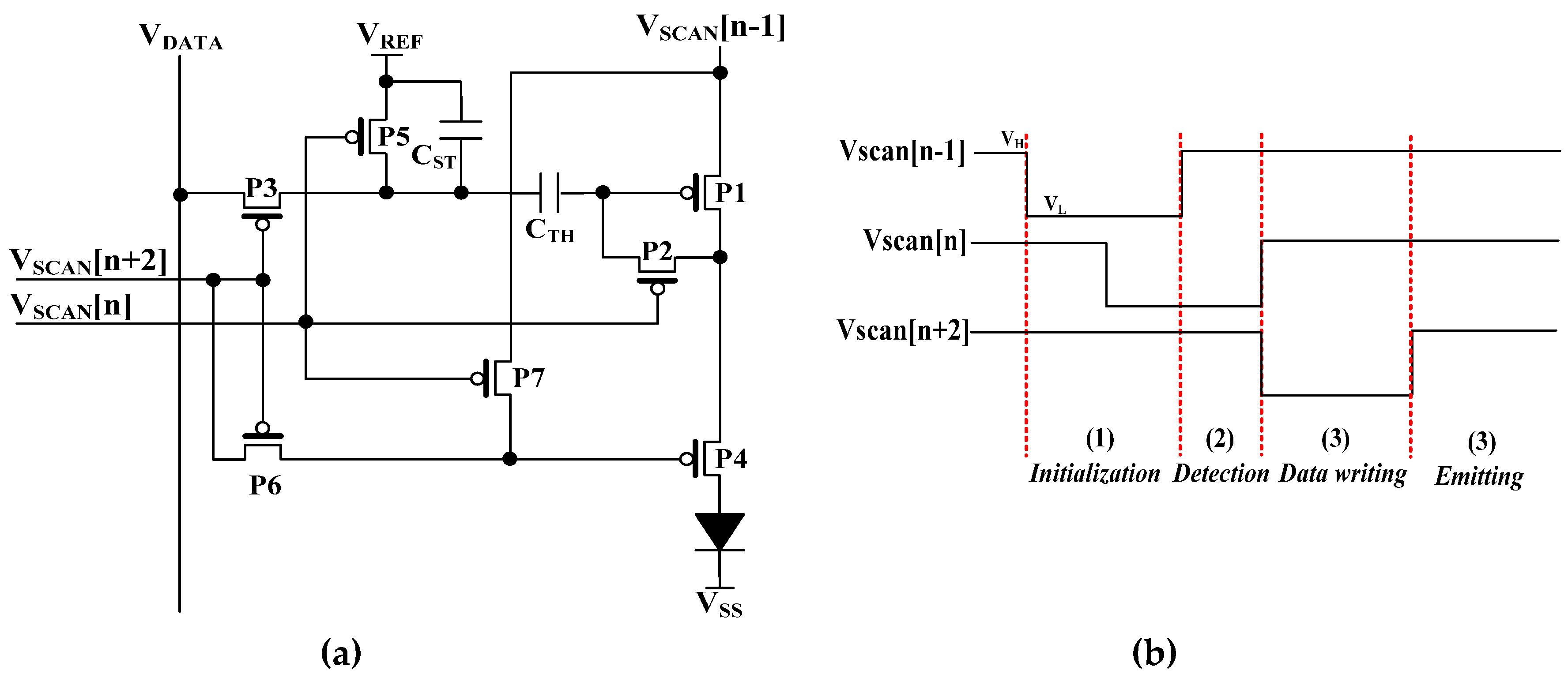
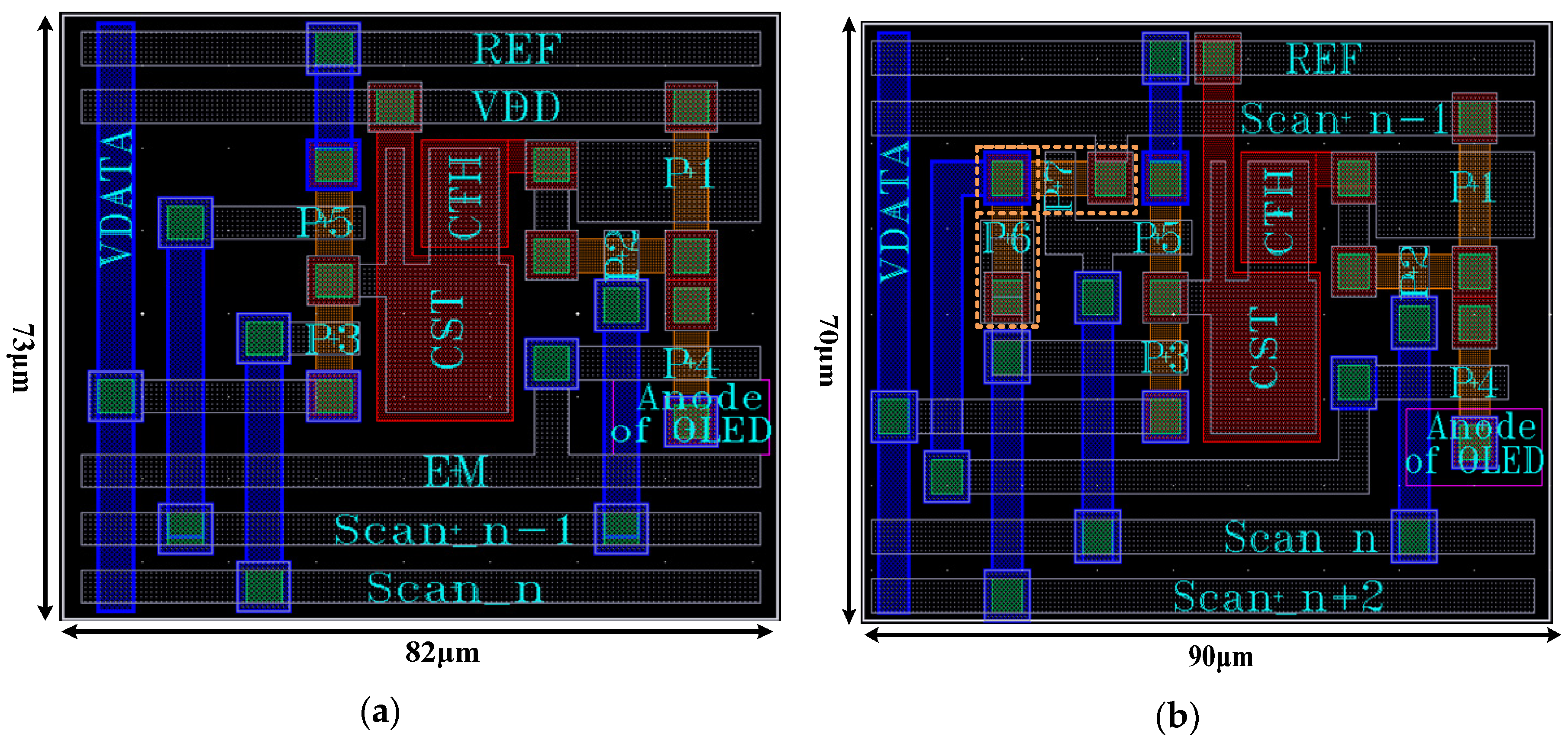
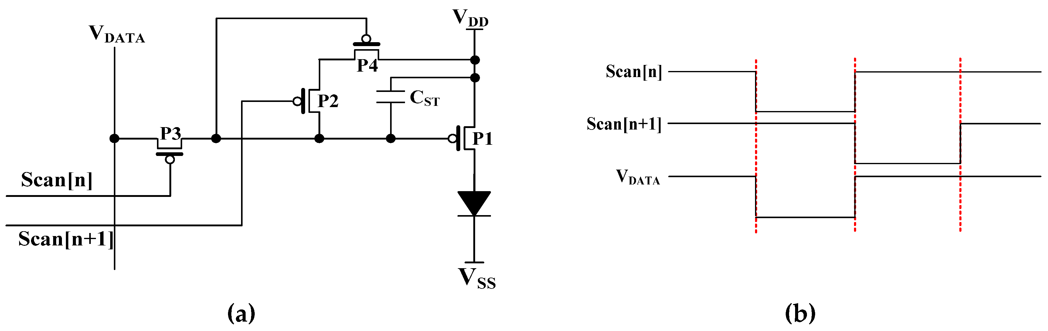
2. Pixel Circuit Description

Figure 1 shows the schematic and timing diagram of proposed pixel circuit, which consists of seven TFTs and the two capacitors (CST and CTH). The specifications for the proposed pixel circuit are shown in Table 2. Here, P1 is the driving transistor, and P2 to P7 are switching transistors. The voltage across CTH is reset by the switching transistors P2, P4, P5, and P7 during the initialization phase. The VTH of P1 and supplied power information are stored by the right terminal of CTH by the turning on of P2 for the detection phase. The data signal is transferred to the left terminal of CTH through P3, and the OLED starts to emit following the negative pulse of VSCAN(n + 2) through the pull-downing of P6. Figure 2 shows the layouts of a single subpixel of the proposed pixel circuit and 5T2C bootstrap pixel circuit [20]. Although the proposed pixel circuit uses more TFTs than 5T2C, the layout area has not increased much, so it has little effect on resolution. The working process of the pixel circuit will be described in detail.

2.1. Initialization Phase

During the initialization phase, P2, P5, and P7 are turned on as both VSCAN(n − 1) and VSCAN(n) are at a low level. Then the gate voltage of P4 is pulled down, and P4 is turned on for resetting the drain electrode of P1 with a relatively low voltage level, i.e., below the turning-on voltage of OLED (VOLED). In addition, the gate and the drain electrodes of the driving transistor P1 are shorted by P2 and the gate voltage of P1 is also discharged through P4, while the left electrode of CTH is initialized with VREF by P5. The electrical hysteresis phenomenon in P-type LTPS transistors should be considered, i.e., the drain-to-source current varies with different gate-sweeping directions, which relates with short-term image sticking issues [21,22]. As CTH is properly initialized before the programming phases, the hysteresis effects can be efficiently suppressed.

2.2. Detection Phase

During the detection phase, P4 is turned off as VSCAN(n − 1) switches to a high level. Then, the gate and the drain electrodes of P1 are gradually charged until the voltage difference between the gate and the source of P1 is VTH. By the end of the detection phase, the gate voltage of P1 approximates the voltage of the power line minus |VTH|. Since P1 operates in the saturation region, the transient response for the gate voltage of P1 can be expressed as:
( C T H + C P 1 _ G S + C P 2 _ G D ) d V G ( t ) d t = 1 2 μ C O X W L [ V H V G ( t ) | V T H | ] 2 ,
where CP1_GS, CP2_GD, μ, COX, W/L, and VH are the gate-to-source capacitance of P1, the gate-to-drain capacitance of P2, field-effective mobility, gate capacitance per unit area, ratio of the channel width to channel length of P1, and the high level of the scan signal, respectively. Assuming the initial value of the P2’s gate electrode as VO, VG can be solved as:
V G ( t ) = V H | V T H | 1 μ C O X W ( t t 0 ) 2 L ( C T H + C P 1 _ G S + C P 2 _ G D ) + 1 V O V H + | V T H | ,
where t0 and t are the start and end times of the charging process, respectively. The compensating efficiency might be reversely affected by the detection accuracy of VTH and VH. As shown in Equation (2), for accurate detection of VTH and VH, a relatively long charging time is required. However, due to the increasing of display resolution, it becomes difficult to extend the detection time.

2.3. Data Writing Phase

During the data writing phase, P3 and P6 are turned on as the levels of Vscan(n − 1) and Vscan(n) are low, and P2, P5, and P7 are turned off as the level of Vscan(n + 2) is high. Then the data voltage, i.e., VDATA, is transferred to the left electrode of CTH through P3. According to the charge conservation law, the voltage at the right electrode of CTH can be expressed as:
V G = V G C P 1 _ G D V G C T H + C P 1 _ G S + C P 1 _ G D + C P 2 _ G D + C T H ( V D A T A V R E F ) C T H + C P 1 _ G S + C P 1 _ G D + C P 2 _ G D ,
Considering that CP1_GD, CP1_GD, and CP2_GD are much smaller than CTH, one can simplify Equation (3) to:
V G = V G + V D A T A V R E F ,

2.4. Emitting Phase

Finally, in the emitting phase, the driving TFT provides the current to OLED pixel, which can be expressed by:
I O L E D = 1 2 μ C O X W L ( V H V G | V T H | ) 2 = 1 2 μ C O X W L ( V H V H + | V T H | + 1 μ C O X W ( t t 0 ) 2 L ( C T H + C P 1 _ G S + C P 2 _ G D ) + 1 V O V H + | V T H | + V R E F V D A T A | V T H | ) 2 = 1 2 μ C O X W L ( V R E F V D A T A + 1 μ C O X W ( t t 0 ) 2 L ( C T H + C P 1 _ G S + C P 2 _ G D ) + 1 V O V H + | V T H | ) 2
Therefore, IOLED is determined by VREF and VDATA, being almost independent of VTH and VH. As shown in Equation (5), the third term in the parenthesis is reversely related with the effective mobility, and then the pixel circuit also renders certain compensation function of mobility non-uniformities. In addition, P4 is maintained off for the initialization and detection phases, the leakage current of the OLED can be suppressed efficiently, and improved contrast ratio with reduced flicker can be obtained.

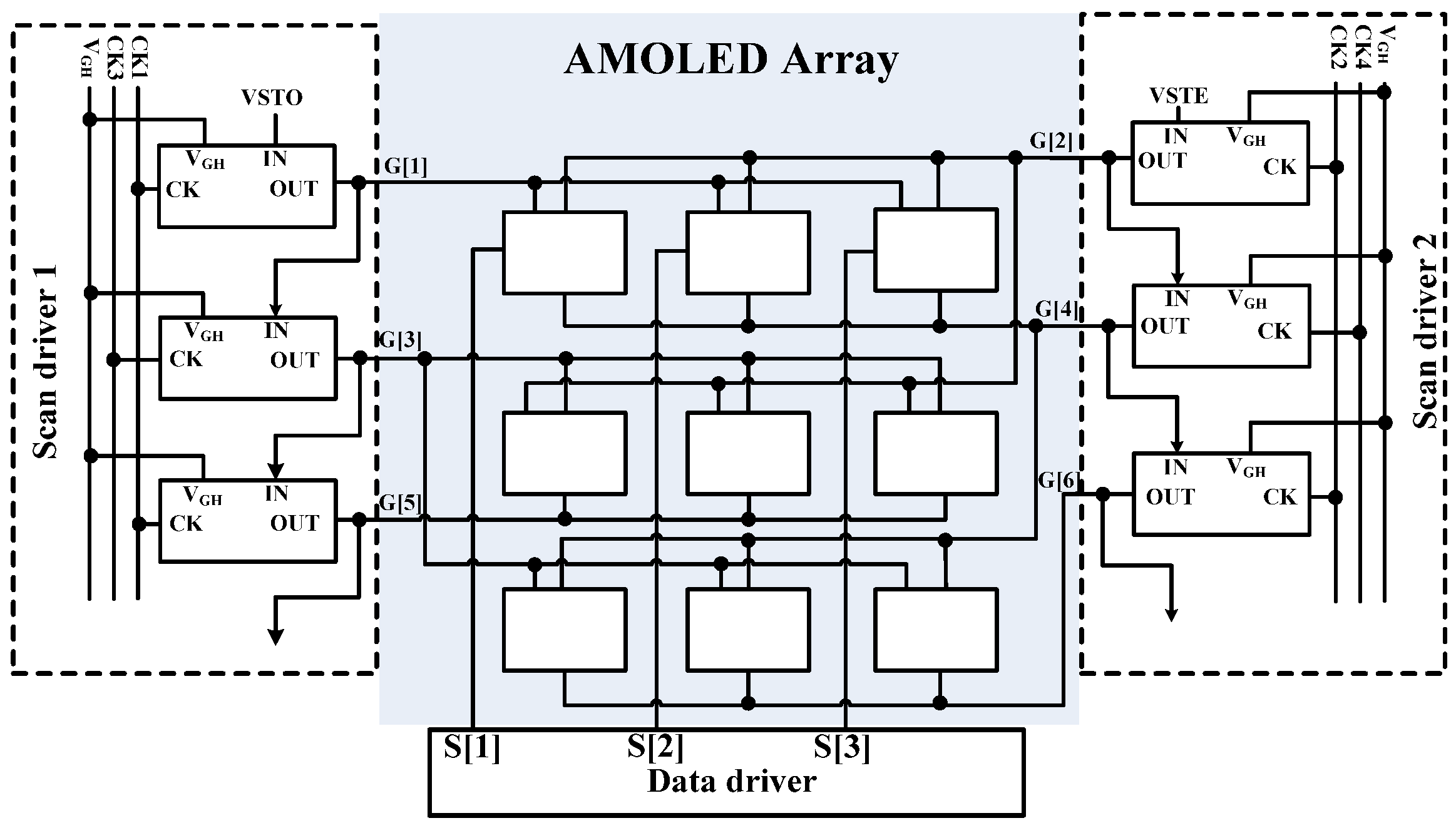
3. Gate Driver Description

For the co-design of pixel circuit and gate driver circuit, the Rensselaer Polytechnic Institute (RPI) model with Level 36 is used to reproduce the electrical performance of the p-type LTPS TFTs. Figure 3 demonstrates the comparison of the measured and simulated transfer characteristics of LTPS TFT in a logarithm scale. Calculated using the classic current-voltage model of MOSFET, the field-effect mobility, the threshold voltage and the sub-threshold swing for the LTPS TFT are approximately 72 cm2 (V·s)−1, −1.1 V, and 0.74 V/decade, respectively.
For the proposed pixel circuit, the high-to-low pulses with line-by-line scanning sequences are needed. Figure 4 shows the gate driver unit, which consists of six TFTs and one capacitor. The parameters of the gate driver unit are shown in Table 3 and the operating mechanism has been detailed elsewhere [23]. In order to generate the required scan signal, four clocks with overlapped waveforms are used. Figure 5 shows the block diagram of the gate driver with detection time half of the scan pulse. The simulation results are illustrated in Figure 6. The devised gate driver circuit is well verified, and a rail-to-rail output range, i.e., from −10 V to 5 V, can be obtained for the gate driver, with the rising and falling times of 1.68 μs and 1.76 μs for loading resistance of 2 KΩ and loading capacitance of 200 pF.

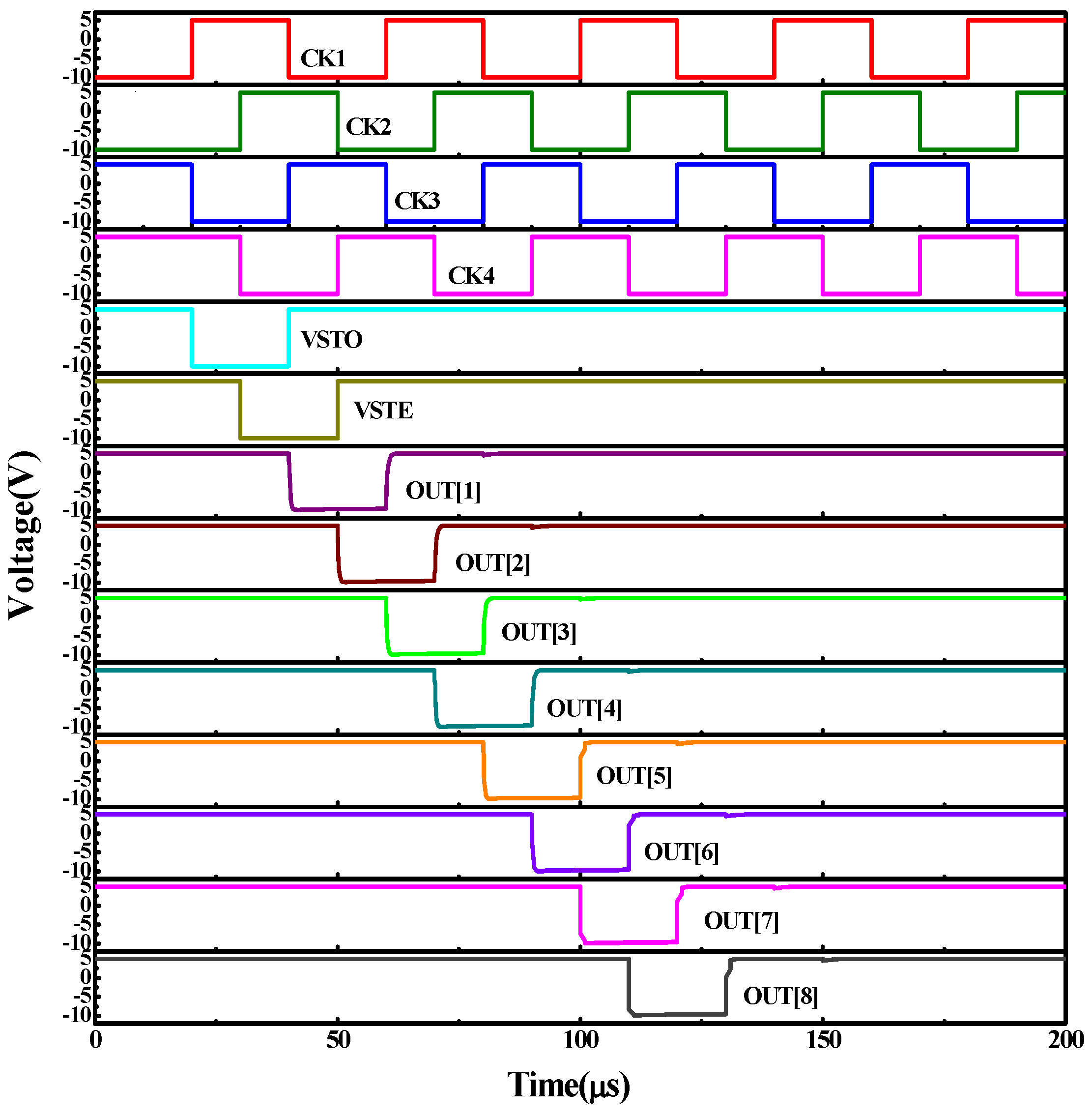
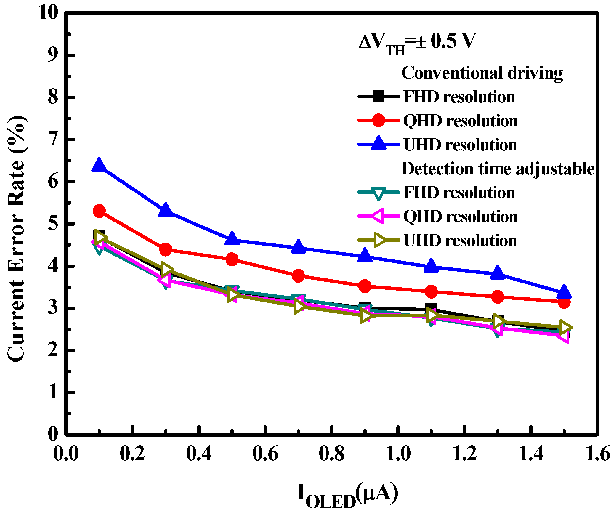
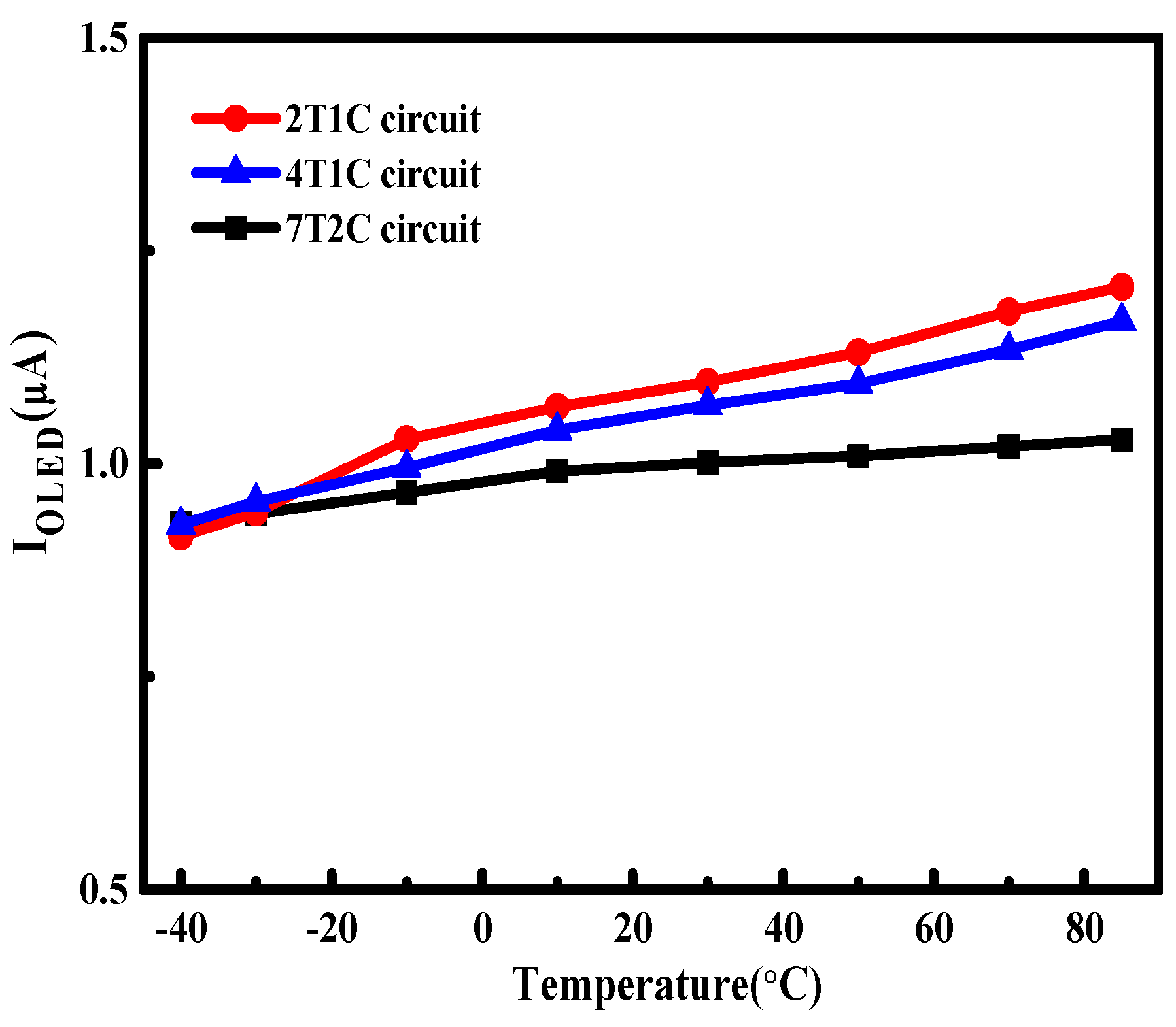
4. Results and Discussion

As mentioned above, a sufficient detection time for VTH and VH is required to improve the compensation accuracy of pixel circuit. However, with the increase of display resolution and frame rate, the detection time for VTH and VH is decreasing. To be more specific, for frame rate of 60 Hz, the row times for the resolution of full-high-definition (FHD) (1920 red–green–blue(RGB)×1080), quad-high definition (QHD) (2560 RGB×1440), and ultra-high-definition (UHD) (3840 RGB×2160), are 15.4 µs, 11.5 µs, and 7.7 µs, respectively. In the proposed circuit, the detection time can be increased by adjusting of the scanning signals. In addition to increase the scan pulse width, modifications of the scanning sequence for the pixel circuit include, replacing the original VSCAN(n − 1) and VSCAN(n + 2) with VSCAN(n − 2) and VSCAN(n + 3), respectively. Then, the detection time is increased from 2 H to 3 H, where 1 H presents the one horizontal time.
Figure 7 shows the comparison of proposed circuit current error rate for different resolutions in conventional driving method (detection time = 1 H) and detection time adjustable driving method (detection time = 2 H). For the conventional driving method, i.e., scan width = 2 H, and detection time =1 H, the current error rate increases for higher resolution. For improved driving method, i.e., scan width = 3 H, and detection time = 2 H, the current error rate is almost independent of the display resolution.
In addition to the length of the detection period, the actual performance of pixel circuit depends on process–voltage–temperature (PVT) factors [24,25], namely the electrical characteristic variations of poly-silicon TFT due to the fabrication process, fluctuations in the power supply, and the distribution of ambient temperature. Due to PVT effects, current-to-voltage curve will shift from the expected one. In the following, PVT influences on the pixel circuit performance with the resolution of 1920 RGB×1080 is investigated. Then, PVT performances of the proposed 7T2C circuit schematic are compared with that of the conventional 2T1C pixel circuit and a 4T1C pixel circuit, which compensates VTH and mobility of the driving TFT through discharging of a mirrored TFT. Figure 8 shows the circuit and timing diagram. The merit of the 4T1C circuit schematic is that the structure is relatively simple, and the required scan and data drive waveforms are as simple as the 2T1C scheme.
Due to the grain boundary and silicon orientation variations, the current-to-voltage characteristics of the poly-Si TFT tend to vary from pixel to pixel. Here, Gaussian statistical distribution is used to model the threshold-voltage of the driving TFT. Monte Carlo simulations were performed for threshold voltage variations of 20% from the nominal values for TFT of 7T2C, 2T1C, and 4T1C pixel circuits and Figure 9 shows Monte Carlo simulation results of the output current error with the sample number of 1000. The mean value of pixel current is 1 μA, and the standard deviations for the pixel current are 4.6 nA, 8.5 nA, and 151.6 nA for the 7T2C, 4T1C, and 4T1C pixel schematics, respectively. These results further confirm that the proposed pixel circuit has higher luminance uniformity and a stronger immunity to process variations than the conventional 2T1C pixel circuit and the 4T1C pixel circuit.
In addition, due to the metal line resistance, voltage drop along the power supply line is inevitable. For larger display panel, the IR drop effect is further deteriorated. Figure 10 shows the current error rate versus IR drop with three pixel circuits. For the conventional 2T1C pixel, abrupt current error rate is caused by IR drop. In the case VH drops from 5 V to 3 V, the current error is reduced to 16.7% and 2.1% for the 4T1C pixel circuit and the 7T2C schematic, respectively. Thus, the proposed pixel circuit shows stronger immunity to the IR drop issue than other pixel circuits, which benefits the implementation of a large-dimension AMOLED panel. For actual products, the operating temperature for AMOLED panels is in the range of −40 degrees to 85 degrees. Figure 11 shows the OLED current versus different temperature for three pixel circuits. The current magnitude is increased by 32.1% and 25.7% with the temperature increase from −40 degrees to 85 degrees for 2T1C and 4T1C circuit. The proposed pixel circuit has much reduced temperature dependence, as the current error is reduced to 10.6% for the temperature variations.

5. Conclusions

This paper proposed a pixel circuit suitable for a narrow border display, which can compensate for threshold voltage non-uniformity and IR drop, and increase the detection time by increasing the signal width at high resolution. The pixel circuit requires mono-type scanning signals, which benefits simplification of the external driving circuit for narrow border displays. The conventional VDD line is replaced by the scanning line to suppress the leakage current for the initial stage. The proposed pixel circuit has a good compensation effect and stability for temperature variations, the simulation results show that the current variation is reduced to 2.1% for the supplied power reduced from 5 V to 3 V, and the current variation is as low as 10.6% for temperatures from −40 degrees to 85 degrees.

Author Contributions

Conceptualization, J.K. and C.L.; methodology, J.K.; software, J.K. and C.L.; validation, J.K.; formal analysis, C.L. and S.H.; investigation, H.L. and Q.W.; writing—original draft preparation, J.K.; writing—review and editing, J.K., C.L., and L.Z.; supervision, L.D. and C.L.; funding acquisition, L.D. All authors have read and agreed to the published version of the manuscript.

Funding

This work was supported in part by the National Key Research and Development Program of China under Grant 2017YFA0204600, and by the Fundamental Research Funds for the Central Universities of Central South University (No. 2019zzts419).

Conflicts of Interest

The authors declare no conflict of interest.

References

  1. Park, C.I.; Seong, M.; Kim, M.A.; Kim, D.; Jung, H.; Cho, M.; Lee, S.H.; Lee, H.; Min, S.; Kim, J.; et al. 54-1: Distinguished Paper: World 1st Large Size 77-inch Transparent Flexible OLED Display. SID Symp. Dig. Tech. Pap. 2018, 49, 710–713. [Google Scholar] [CrossRef]
  2. Seol, H.-C.; Ra, J.-H.; Hong, S.-K.; Kwon, O.-K. An AMOLED Panel Test System Using Universal Data Driver ICs for Various Pixel Structures. IEEE Trans. Electron. Devices 2016, 64, 189–194. [Google Scholar] [CrossRef]
  3. Qin, T.; Liao, C.; Huang, S.; Yu, T.; Deng, L. Analytical drain current model for symmetric dual-gate amorphous indium gallium zinc oxide thin-film transistors. Jpn. J. Appl. Phys. 2017, 57, 14301. [Google Scholar] [CrossRef]
  4. Li, C.; Liao, C.-W.; Yu, T.-B.; Ke, J.-Y.; Huang, S.; Deng, L. Concise Modeling of Amorphous Dual-Gate In-Ga-Zn-O Thin-Film Transistors for Integrated Circuit Designs. Chin. Phys. Lett. 2018, 35, 027302. [Google Scholar] [CrossRef]
  5. Lin, C.L.; Chen, P.S.; Chen, H.M.; Chen, F.H. A novel p-Type LTPS TFT pixel circuit compensating for threshold voltage and mobility variations. J. Disp. Tech. 2014, 10, 995–1000. [Google Scholar]
  6. Wadhwa, N.; Bahubalindruni, P.G.; Chapagai, K.; Goes, J.; Deb, S.; Barquinha, P. Sixth-order differential Sallen-and-Key switched capacitor LPF using a-IGZO TFTs. Int. J. Circuit Theory Appl. 2018, 47, 32–42. [Google Scholar] [CrossRef] [Green Version]
  7. Keum, N.-H.; Oh, K.; Hong, S.-K.; Kwon, O.-K. A Pixel Structure Using Block Emission Driving Method for High Image Quality in Active Matrix Organic Light-Emitting Diode Displays. J. Disp. Technol. 2016, 12, 1250–1256. [Google Scholar] [CrossRef]
  8. Fan, C.-L.; Chen, Y.-C.; Yang, C.-C.; Tsai, Y.-K.; Huang, B.-R. Novel LTPS-TFT Pixel Circuit with OLED Luminance Compensation for 3D AMOLED Displays. J. Disp. Technol. 2016, 12, 425–428. [Google Scholar] [CrossRef]
  9. Wu, W.; Zhou, L.; Yao, R.-H.; Peng, J.-B. A New Voltage-Programmed Pixel Circuit for Enhancing the Uniformity of AMOLED Displays. IEEE Electron. Device Lett. 2011, 32, 931–933. [Google Scholar] [CrossRef]
  10. Park, J.; Fujii, M.; Moon, J.; Wang, I. The method to compensate IR-drop of AMOLED display. SID Symp. Dig. Tech. Pap. 2018, 40, 983–985. [Google Scholar] [CrossRef]
  11. In, H.-J.; Kwon, O.-K. A Simple Pixel Structure Using Polycrystalline-Silicon Thin-Film Transistors for High-Resolution Active-Matrix Organic Light-Emitting Diode Displays. IEEE Electron. Device Lett. 2012, 33, 1018–1020. [Google Scholar] [CrossRef]
  12. Liao, C.; Deng, W.; Song, D.; Huang, S.; Deng, L. Mirrored OLED pixel circuit for threshold voltage and mobility compensation with IGZO TFTs. Microelectron. J. 2015, 46, 923–927. [Google Scholar] [CrossRef]
  13. Ashtiani, S.J.; Servati, P.; Striakhilev, D.; Nathan, A. A 3-TFT Current-Programmed Pixel Circuit for AMOLEDs. IEEE Trans. Electron. Devices 2005, 52, 1514–1518. [Google Scholar] [CrossRef]
  14. Chaji, G.; Nathan, A. A Fast Settling Current Driver Based on the CCII for AMOLED Displays. J. Disp. Technol. 2005, 1, 283–288. [Google Scholar] [CrossRef]
  15. In, H.-J.; Oh, K.-H.; Lee, I.; Ryu, D.-H.; Choi, S.-M.; Kim, K.-N.; Kim, H.-D.; Kwon, O.-K. An Advanced External Compensation System for Active Matrix Organic Light-Emitting Diode Displays With Poly-Si Thin-Film Transistor Backplane. IEEE Trans. Electron. Devices 2010, 57, 3012–3019. [Google Scholar] [CrossRef]
  16. Bang, J.-S.; Kim, H.-S.; Kim, K.-D.; Kwon, O.-J.; Shin, C.-S.; Lee, J.; Cho, G.-H. A Hybrid AMOLED Driver IC for Real-Time TFT Nonuniformity Compensation. IEEE J. Solid-state Circuits 2016, 51, 966–978. [Google Scholar]
  17. Lin, C.-C.; Yen, S.; Hsu, S.-Y.; Kuo, T.-W.; Lee, T.-S.; Liu, C.-H.; Lin, S.-L.; Hsiao, H.-Y.; Kung, C.-H.; Yeh, Y.-F.; et al. 7–3: AMOLED Pixel Structure Using the Close Loop Negative Feedback Method for High Resolution Displays. SID Symp. Dig. Tech. Pap. 2016, 47, 61–64. [Google Scholar] [CrossRef]
  18. Lee, J.-P.; Jeon, H.-S.; Moon, D.-S.; Bae, B.S. Threshold Voltage and IR Drop Compensation of an AMOLED Pixel Circuit Without a VDD Line. IEEE Electron. Device Lett. 2013, 35, 72–74. [Google Scholar] [CrossRef]
  19. Lin, C.-L.; Lai, P.-C.; Shih, L.-W.; Hung, C.-C.; Lai, P.-C.; Lin, T.-Y.; Liu, K.-H.; Wang, T.-H. Compensation Pixel Circuit to Improve Image Quality for Mobile AMOLED Displays. IEEE J. Solid-state Circuits 2018, 54, 489–500. [Google Scholar] [CrossRef]
  20. Kim, Y.W.; Kwak, W.K.; Lee, J.Y.; Choi, W.S.; Lee, K.Y.; Kim, S.C.; Yoo, E.J. 9.1: 40 Inch FHD AM-OLED Display with IR Drop Compensation Pixel Circuit. SID Symp. Dig. Tech. Pap. 2009, 40, 85. [Google Scholar] [CrossRef]
  21. Lee, J.; Choi, B. Effects of Channel Type and Doping on Hysteresis in Low-Temperature Poly-Si Thin-Film Transistors. IEEE Trans. Electron. Devices 2018, 65, 986–994. [Google Scholar] [CrossRef]
  22. Hwang, H.W.; Hong, S.; Hwang, S.S.; Kim, K.W.; Ha, Y.M.; Kim, H.J. Analysis of Recoverable Residual Image Characteristics of Flexible Organic Light-Emitting Diode Displays Using Polyimide Substrates. IEEE Electron. Device Lett. 2019, 40, 1108–1111. [Google Scholar] [CrossRef]
  23. Chen, M.; Lei, J.; Huang, S.; Liao, C.; Deng, L. Poly-Si TFTs integrated gate driver circuit with charge-sharing structure. J. Semicond. 2017, 38, 55001. [Google Scholar] [CrossRef]
  24. Radfar, M.; Shah, K.; Singh, J. A highly sensitive and ultra low-power forward body biasing circuit to overcome severe process, voltage and temperature variations and extreme voltage scaling. Int. J. Circuit Theory Appl. 2013, 43, 233–252. [Google Scholar] [CrossRef]
  25. Anthony, B.; Xavier, A.; Frederic, C.; Dominique, D.; Jean, B.B. A robust inverter-based amplifier versus PVT for discrete-time integrators. Int. J. Circuit Theory Appl. 2018, 46, 2160–2169. [Google Scholar]
Figure 1. The proposed active matrix organic light-emitting diode (AMOLED) pixel circuit. (a) The circuit schematic, and (b) the timing diagram. VTH: threshold voltage; VDATA: data voltage.
Electronics 09 00574 g001
Figure 2. Layout of the pixel circuit. (a) The 5T2C bootstrap pixel circuit, and (b) the proposed AMOLED pixel circuit.
Electronics 09 00574 g002
Figure 3. Measured and simulated transfer characteristics of the low-temperature poly-silicon thin-film transistor (LTPS TFT) with an aspect ratio of 4 μm/4 μm. COX: gate capacitance per unit area; μ: field-effective mobility; SS: sub-threshold swing.
Electronics 09 00574 g003
Figure 4. The integrated gate driver unit, with (a) the schematic, and (b) the timing diagram.
Electronics 09 00574 g004
Figure 5. The block diagram of the proposed gate driver circuit.
Electronics 09 00574 g005
Figure 6. The transient response of the proposed gate driver circuit with RL = 2 KΩ and CL = 200 pF.
Electronics 09 00574 g006
Figure 7. Current error rate versus IOLED for different driving schemes with various resolution formats. FHD: full-high-definition; QHD: quad-high definition; UHD: ultra-high-definition.
Electronics 09 00574 g007
Figure 8. The mirror-discharge based AMOLED pixel circuit, with (a) the pixel schematic, and (b) the timing diagram.
Electronics 09 00574 g008
Figure 9. Monte Carlo analysis of the emission current with VTH in a Gaussian statistical distribution when the relative error is 20%. (a) The conventional 2T1C pixel circuit, (b) the 4T1C pixel circuit, and (c) the proposed pixel circuit.
Electronics 09 00574 g009
Figure 10. Evolution of IOLED error rate versus increased IR drop.
Electronics 09 00574 g010
Figure 11. Evolution of IOLED versus temperature.
Electronics 09 00574 g011
Table 1. Comparison among the proposed and previous pixel circuits. TFT: thin-film transistor.
ReferenceTFT NumberTFT TypeNumber of Scan LinesScanning Signal TypesFlicker PreventionDetection Time Extension
[5]6T1Cp-type, poly-Si 33NoYes
[7]5T2Cp-type, poly-Si33YesYes
[8]5T2Cp-type, poly-Si44YesYes
[9]5T2Cn-type, a-Si:H 33YesYes
[11]3T2Cp-type, poly-Si22NoNo
[17]5T2Cp-type, poly-Si33YesYes
This work 7T2Cp-type, poly-Si21YesYes
Table 2. Parameters of the proposed pixel circuit.
ParameterValueParameterValue
W/L (P1)4 μm/10 μmW/L (P7)4 μm/4 μm
W/L (P2)4 μm/4 μmVSCA−10–5 V
W/L (P3)4 μm/4 μmVSS−4 V
W/L (P4)4 μm/4 μmVREF−1 V
W/L (P5)4 μm/4 μmCTH0.1 pF
W/L (P6)4 μm/4 μmCST0.3 pF
Table 3. Parameters of the gate driver circuit.
ParameterValueParameterValue
W/L (G1)500 μm/4 μmW/L (G6)10 μm/4 μm
W/L (G2)30 μm/4 μmC10.8 pF
W/L (G3)20 μm/4 μmCK−10–5 V
W/L (G4)10 μm/4 μmIN−10–5 V
W/L (G5)10 μm/4 μmVGH5 V

