Article

Differential Bi-Level Microstrip Directional Coupler with Equalized Coupling Coefficients for Directivity Improvement

by
Slawomir Gruszczynski
*,
Robert Smolarz
and
Krzysztof Wincza
Department of Electronics, AGH University of Science and Technology, 30-059 Krakow, Poland
*
Author to whom correspondence should be addressed.
Electronics 2020, 9(4), 547; https://doi.org/10.3390/electronics9040547
Submission received: 10 March 2020 / Revised: 20 March 2020 / Accepted: 23 March 2020 / Published: 25 March 2020
(This article belongs to the Special Issue RF/Mm-Wave Circuits Design and Applications)

Abstract

:
In this paper, a bi-level microstrip differential directional coupler has been investigated. It has been shown that the equalization of coupling coefficients can be successfully made with the use of appropriate dielectric stack-up and conductor geometry. The application of additional top dielectric layer can ensure proper equalization of coupling coefficients by lowering the value of capacitive coupling coefficient to the value of the inductive one. The theoretically investigated coupled-line section has been used for the design of a 3-dB differential directional coupler. The measurement results are compared with the theoretical ones.

1. Introduction

Recently differential directional couplers are of interest of microwave engineering community, and find applications, e.g., in mixer or VCO design [1,2]. One can find the examples of branch-line differential directional couplers [3,4,5,6,7,8]. Such couplers are known as being narrow-band networks having simultaneously large size. In contrary, coupled-line directional couplers feature larger bandwidths with smaller sizes, and recently it was shown that such couplers can also be designed as differential ones [9,10,11,12]. Until now the differential coupled-line directional couplers have been designed in homogeneous dielectric media in which the capacitive and inductive coupling coefficients are balanced, and hence good directive properties can be obtained [11]. It was also shown in [12] that a coupled-line directional coupler can be designed in inhomogeneous dielectric medium and can be compensated with the quasi-lumped element approach. Furthermore, a method for compensation of modal phase velocities has been shown for the special case of symmetric directional couplers in inhomogeneous stripline technique [13].
In this paper, we show for the first time the possibility of coupling coefficients’ equalization in multilayer-microstrip coupled-line geometry using the technique known for single-ended directional couplers, i.e., by the utilization of appropriate dielectric stratification. We show in the paper that the additional top dielectric layer can provide the required coupling coefficients’ equalization by lowering the capacitive coupling coefficient, while not influencing the inductive one. The theoretical investigation has been supported with the measurements of a 3-dB differential directional coupler designed for the center frequency of 1.4 GHz.

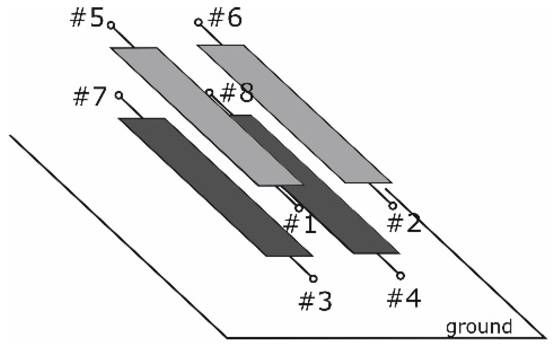
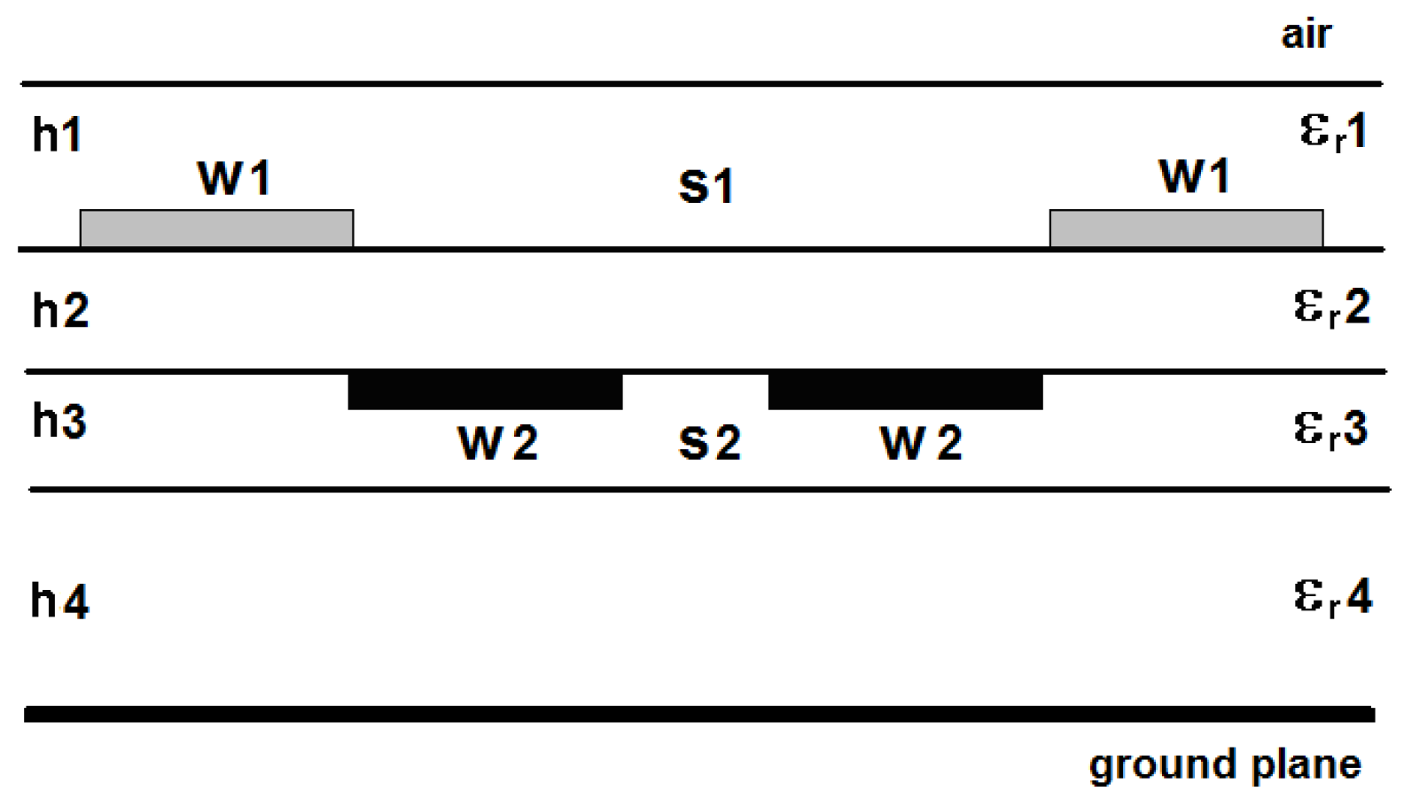
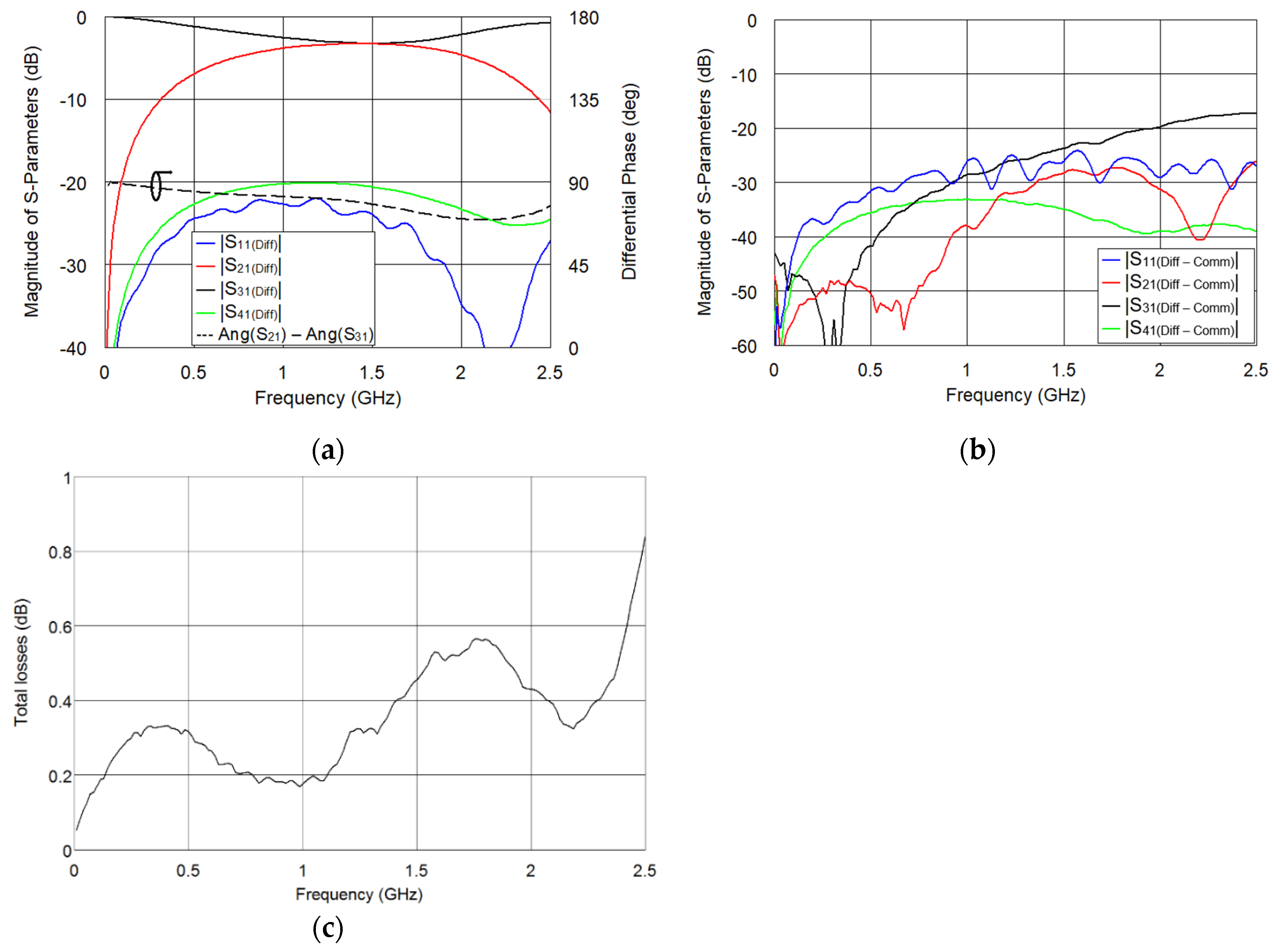
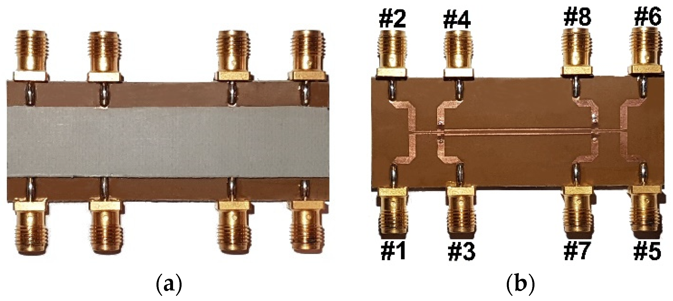
2. Analysis and Design

The investigation on the design of a differentially-fed coupled-line directional coupler has been carried out, based on the previously published work on the design of such directional couplers in homogeneous dielectric medium [11]. Here, we took the effort to verify the possibility of designing such directional couplers in inhomogeneous dielectric media, which is in particular useful, when microstrip structures are considered. A conceptual view of a four-strip coupled-line system is shown in Figure 1, whereas, proposed coupled-line geometry is presented in Figure 2, and consists of a base substrate, having thickness h4, a substrate having thickness h2 on which the traces of the coupler are etched. Moreover, two additional layers are present, among which the layer having thickness h3 is purely technological layer bonding the two layers h4 and h2 together, while the top layer is a compensating layer.
In the directional coupler’s design, the following procedure has been utilized:
  • The coupled-line geometry, shown in Figure 2, has been numerically analyzed, in our research the Linpar software has been used [14].
  • From the numerical analysis the 4 × 4 per-unit-length inductive and capacitive matrices of a coupled-line system have been found.
  • The 4 × 4 matrices have been reduced to 2 × 2 matrices of the equivalent two conductor coupled-line section with the formulas derived in [11].
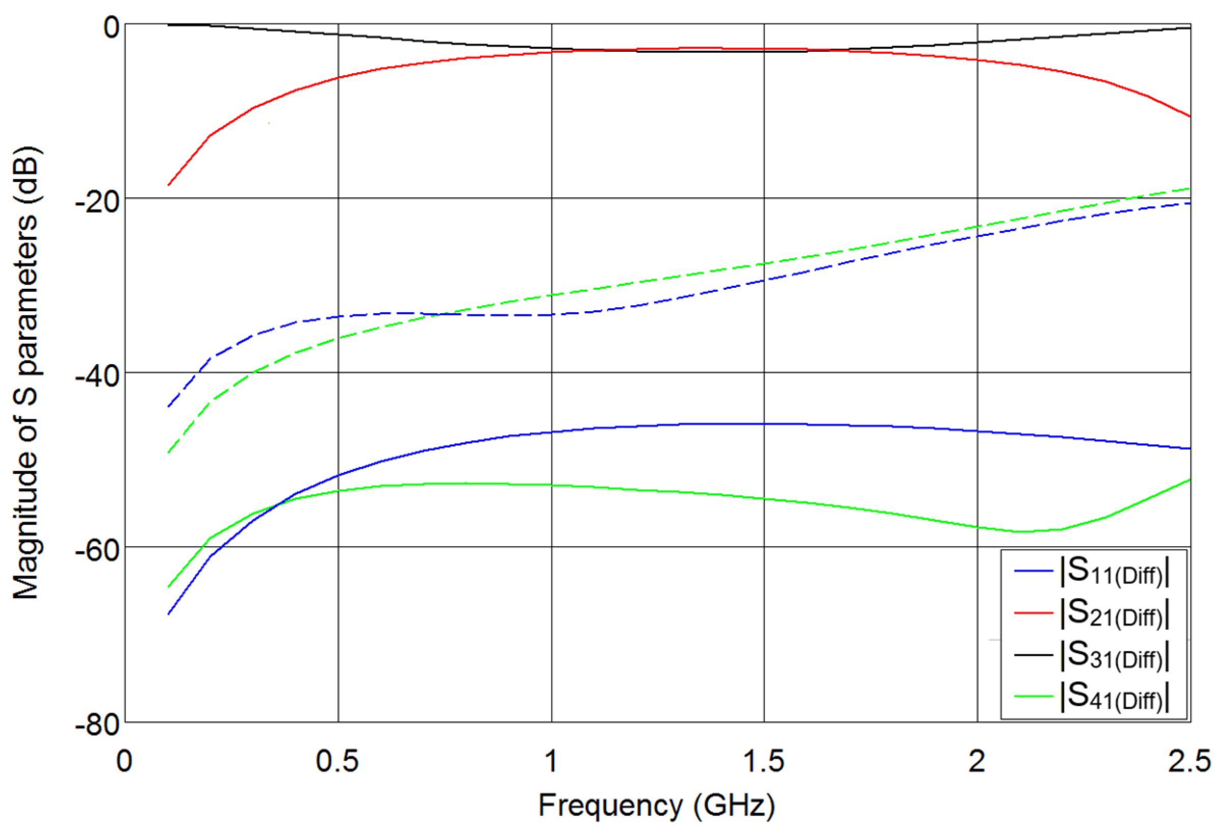
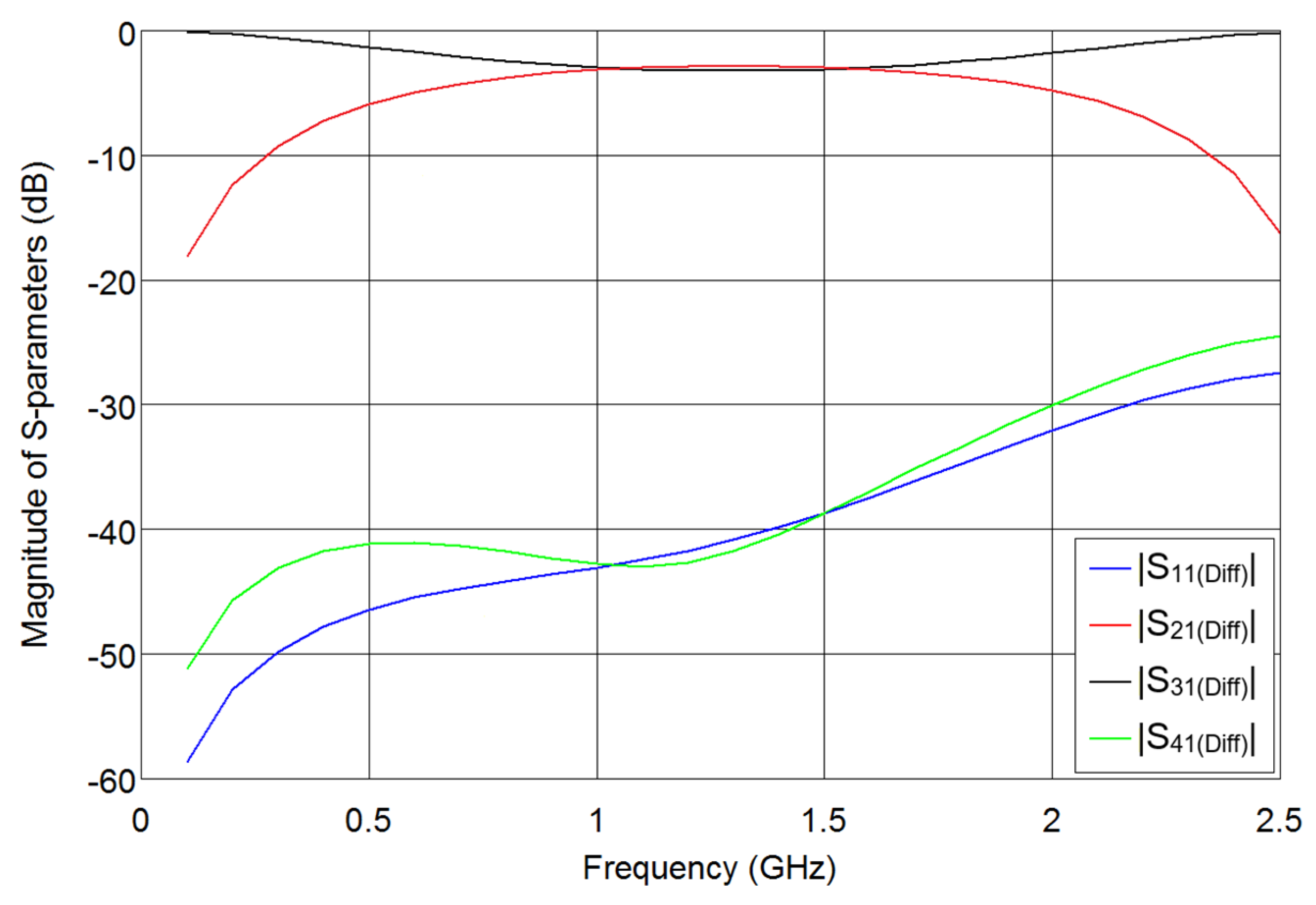
The geometry has been iteratively optimized in order to obtain the required coupling coefficients and impedances of the conductor pairs.
In the first step of the design a coupled-line geometry has to be found for which the inductive coupling coefficient and characteristic impedances of the lines are as desired for the final coupler. Since the overlay dielectric layer h1 will be used for the compensation, the inductive coupling coefficient will not be modified. Additionally, when selecting an initial geometry without top compensating layer the capacitive coupling coefficient has to be greater than the inductive one, since the dielectric overlay will lower the capacitive coupling coefficient to be equal to inductive one. For our analysis the following parameters of the coupled line geometry have been found: h4 = 0.76 mm, εr4 = 4.5, h3 = 0.09 mm, εr3 =3.38, h2 = 0.05 mm, εr2 = 3.4, for which the above mentioned criteria are met.
In the second step the process of described iterative calculations is applied. In our calculations the following geometrical parameters have been found: the strip widths and the spacing for the top balanced line equal w1 = 0.345 mm, s1 = 1 mm, and the strip widths and spacing for the bottom balanced line are w2 = 0.315 mm, s2 = 0.6 mm. Furthermore, the top dielectric layer has been optimized in order to equalize capacitive and inductive coupling coefficients and the following values have been obtained: h1 = 0.787 mm, εr1 = 2.5. The optimized geometry features differential characteristic impedance Z0 = 100 Ω and coupling coefficients kL = kC = 0.705.
The overlay dielectric layer h1 provides for capacitive and inductive coupling coefficients’ equalization, which is a necessary condition for the realization of an ideal coupled line section [15], and hence it is a necessary condition to obtain good isolation and impedance match of the coupled-line section. To illustrate the compensating effects of the top dielectric layer on the chosen coupled-line geometry the influence of the layer’s thickness and dielectric constant have been calculated and the results are shown in Figure 3.
As it is seen both the thickness and the dielectric constant of the top layer influence the capacitive coupling coefficient. The inductive coupling coefficient is not influenced, since it depends on conductor geometry only, and can be calculated from the capacitive matrix of the homogeneous air filled geometry (not depending on any dielectric properties). The application of additional dielectric layer lowers the capacitive coupling coefficient and it is required to adjust the parameters h1 and εr1 to obtain equity of both inductive and capacitive coefficients.
The designed coupled-line geometry has been further investigated and scattering parameters of a coupled line section have been calculated electromagnetically with the AWR Microwave Office software. The results are shown in Figure 4 with comparison to the equivalent section with removed compensating top dielectric layer. As it is seen, the application of the compensating layer improves the isolation and impedance match by about 20 dB. Further, the scattering parameters of the complete directional coupler with transitions between coupled and uncoupled lines have been calculated electromagnetically, and are shown in Figure 5. The designed directional coupler features equal power split between direct and coupled ports (k ≅ 0.7), the return losses and isolation are better than 40 dB at the center frequency.
Finally, the directional coupler has been fabricated and measured with the Keysight PNA-X N5224 four port vector network analyzer. The analyzer has been calibrated at the male connector planes with the Short-Open-Load-Through calibration technique and Keysight 85052D manual calibration kit. The single-ended measurement results have been recalculated to the differential ones and are presented in Figure 6. The obtained return losses are not worse than 22 dB, whereas the isolation is better than 20 dB. The coupler features equal power split. The conversion losses between differential and common modes are better that 25 dB at the center frequency and the total losses do not exceed 0.4 dB at the center frequency. The difference between measured and simulated results, especially in terms of return loss and isolation levels may result from the fact that additional transmission line sections have been added to the fabricated model to allow for connector attachment. The lines have been de-embedded from the measured results. Further, the connector-microstrip line transitions were not included in the simulations, which can introduce additional mismatch seen in the measured results, and also the limited accuracy of lithography process can have impact on the coupled-line geometry modifying the characteristic impedances of the coupled lines. The picture of the fabricated model is shown in Figure 7.

3. Conclusions

A novel differential bi-level microstrip directional coupler has been investigated. It was shown that such coupled-line sections can be successfully compensated, and capacitive and inductive coupling coefficients can be equalized with additional dielectric layer. The application of the additional layer lowers the capacitive coupling coefficient and the parameters of this layer can be selected for proper equalization. The theoretically investigated directional coupler has been fabricated and measured. The obtained measurement results are in agreement with the calculated ones. A noticeable deterioration of isolation and return losses is related to the mismatch at the coaxial-microstrip transitions and the limited manufacturing accuracy of the directional coupler.

Author Contributions

Conceptualization S.G. and K.W. Investigation, R.S.; Methodology, K.W., S.G.; Supervision, S.G.; Writing – original draft, S.G., R.S. and K.W. All authors have read and agreed to the published version of the manuscript.

Funding

This work was partially supported by the National Science Centre Poland under contract no. UMO-2016/21/B/ST7/02200 and in part by the Polish Ministry of Science and Higher Education under subvention funds for the Department of Electronics of AGH.

Conflicts of Interest

The authors declare no conflict of interest.

References

  1. Ng, H.J.; Jahn, M.; Feger, R.; Wagner, C.A. Stelzer: An efficient SiGe double-balanced mixer with a differential rat-race coupler. In Proceedings of the European Microwave Conference, Nurnberg, Germany, 6–10 October 2013. [Google Scholar]
  2. Shi, Q.; Vaesen, K.; Parvais, B.; Mangraviti, G.; Wambacq, P. A 54–69.3 GHz dual-band VCO with differential hybrid coupler for quadrature generation. In Proceedings of the IEEE Asian Solid-State Circuits Conference (A-SSCC), Singapore, 11–13 November 2013. [Google Scholar]
  3. Shi, J.; Qiang, J.; Xu, K.; Wang, Z.B.; Lin, L.; Chen, J.X.; Liu, W. A balanced filtering branch-line coupler. IEEE Microw. Wirel. Compon. Lett. 2016, 26, 119–121. [Google Scholar] [CrossRef]
  4. Shi, J.; Qiang, J.; Cao, Q. Single-layer balanced branch-line coupler. In Proceedings of the IEEE 5th Asia Pacific Conference on Antennas and Propagation APCAP, Kaohsiung, Taiwan, 26–29 July 2016. [Google Scholar]
  5. Duan, X.; Feng, W.; Zhao, Y.; Che, W.; Gomez-Garcia, R. Single-band balanced coupler with wideband common-mode suppression. In Proceedings of the International Conference on Microwave and Millimeter Wave Technology (ICMMT), Chengdu, China, 7–11 May 2018. [Google Scholar]
  6. Chang, C.C.; Pang, Y.H. Dual-band balanced-to-balanced rat-race coupler with bandpass response. In Proceedings of the IEEE Asia Pacific Microwave Conference (APMC), Kuala Lumpur, Malaysia, 13–16 November 2017. [Google Scholar]
  7. Wang, Y.; Ma, K.; Mou, S. A transformer-based 3-dB differential coupler. IEEE Trans. Microw. Theory Tech. 2018, 65, 2151–2159. [Google Scholar] [CrossRef]
  8. Shi, J.; Qiang, J.; Xu, K.; Qin, W.; Zhou, L.; Cao, Q. A differential branch-line coupler. In Proceedings of the IEEE 4th Asia-Pacific Conference on Antennas and Propagation (APCAP), Kuta, Indonesia, 30 June–3 July 2015. [Google Scholar]
  9. Vioneau, F.; Martineau, B.; Sie, M.; Ghiotto, A.; Kerherve, E. A differential vertical hybrid coupler and low capacitance RF pads form millimeter-wave applications in 28 nm CMOS FDSOI. In Proceedings of the IEEE 18th Topical Meeting on Silicon Monolithic Integrated Circuits in RF Systems (SiRF), Anaheim, CA, USA, 14–17 January 2018; pp. 57–59. [Google Scholar]
  10. Hamed, K.W.; Freundorfer, A.P.; Antar, Y.M.M. A new broadband monolithic passive differential coupler for K/ka-band applications. IEEE Trans. Microw. Theory Tech. 2006, 54, 2527–2533. [Google Scholar] [CrossRef]
  11. Janisz, K.; Piekarz, I.; Staszek, K.; Wincza, K.; Gruszczynski, S. Differentially fed directional couplers with coupled-conductors of unequal widths. IEEE Microw. Wirel. Comp. Lett. 2018, 28, 759–761. [Google Scholar] [CrossRef]
  12. Piekarz, I.; Sorocki, J.; Wincza, K.; Gruszczynski, S.; Papapolymerou, J. High-performance differentially fed coupled-line directional couplers realized in inhomogeneous medium. IET Microw. Antennas Propag. 2019, 13, 2005–2012. [Google Scholar] [CrossRef]
  13. Smolarz, R.; Wincza, K.; Gruszczynski, S. Modal phase velocity compensation in multilayer differentially-fed directional couplers. Microw. Opt. Technol. Lett. 2020. [Google Scholar] [CrossRef]
  14. Djordjevic, A.R.; Bazdar, M.B.; Sarkar, T.K.; Harrington, R.F. Matrix Parameters for Multiconductor Transmission Lines, Software and User’s Manual; Artech House: Norwood, MA, USA, 1989. [Google Scholar]
  15. Sachse, K. The scattering parameters and directional coupler analysis of characteristically terminated asymmetric coupled transmission lines in an inhomogeneous medium. IEEE Trans. Microw. Theory Tech. 1990, 38, 417–425. [Google Scholar] [CrossRef]
Figure 1. A conceptual view of a four-strip coupled-line system which can operate as differentially-fed coupled-line directional coupler, having differential excitation provided between the appropriate balanced ports: #1 and #2, #3 and #4, #5 and #6, #7 and #8.
Electronics 09 00547 g001
Figure 2. Cross-sectional view of a multilayer dielectric structure used for the design of differential bi-level microstrip 3-dB directional coupler.
Electronics 09 00547 g002
Figure 3. Calculated inductive kL (dashed lines) and capacitive kC (solid lines) coupling coefficients for the coupled line geometry in which the following parameters have been chosen: h4 = 0.76 mm, εr4 = 4.5, h3 = 0.09 mm, εr3 =3.38, h2 = 0.05 mm, εr2 = 3.4, w1 = 0.345 mm, s1 = 1mm, w2 = 0.315 mm, s2 = 0.6. Analysis of the geometry vs. the thickness h1 of the top layer assuming dielectric constant εr1 = 2.5, and similar analysis vs. the dielectric constant εr1 of the top layer for the thickness h1 = 0.787.
Electronics 09 00547 g003
Figure 4. Electromagnetically calculated differential S-parameters of the four strip coupled-line section operating in a differential mode: the compensated section is represented by solid lines and uncompensated one by dashed lines.
Electronics 09 00547 g004
Figure 5. Electromagnetically calculated differential S-parameters of the compensated differential coupled-line directional coupler.
Electronics 09 00547 g005
Figure 6. Measured magnitudes of differential S-parameters (solid lines) and phase characteristic (dashed line) (a), differential-to-common mode S-parameters (b) and the measured total losses (c) of the manufactured compensated differential coupled-line directional coupler.
Electronics 09 00547 g006
Figure 7. Photograph of the manufactured 3-dB differentially-fed directional coupler (a), and the coupler with the top compensating dielectric layer removed, showing the coupled traces and ports’ labeling (b).
Electronics 09 00547 g007

