A CMOS Data Transfer System Based on Planar RF Coupling for Reinforced Galvanic Isolation with 25-kV Surge Voltage and 250-kV/µs CMTI


Abstract
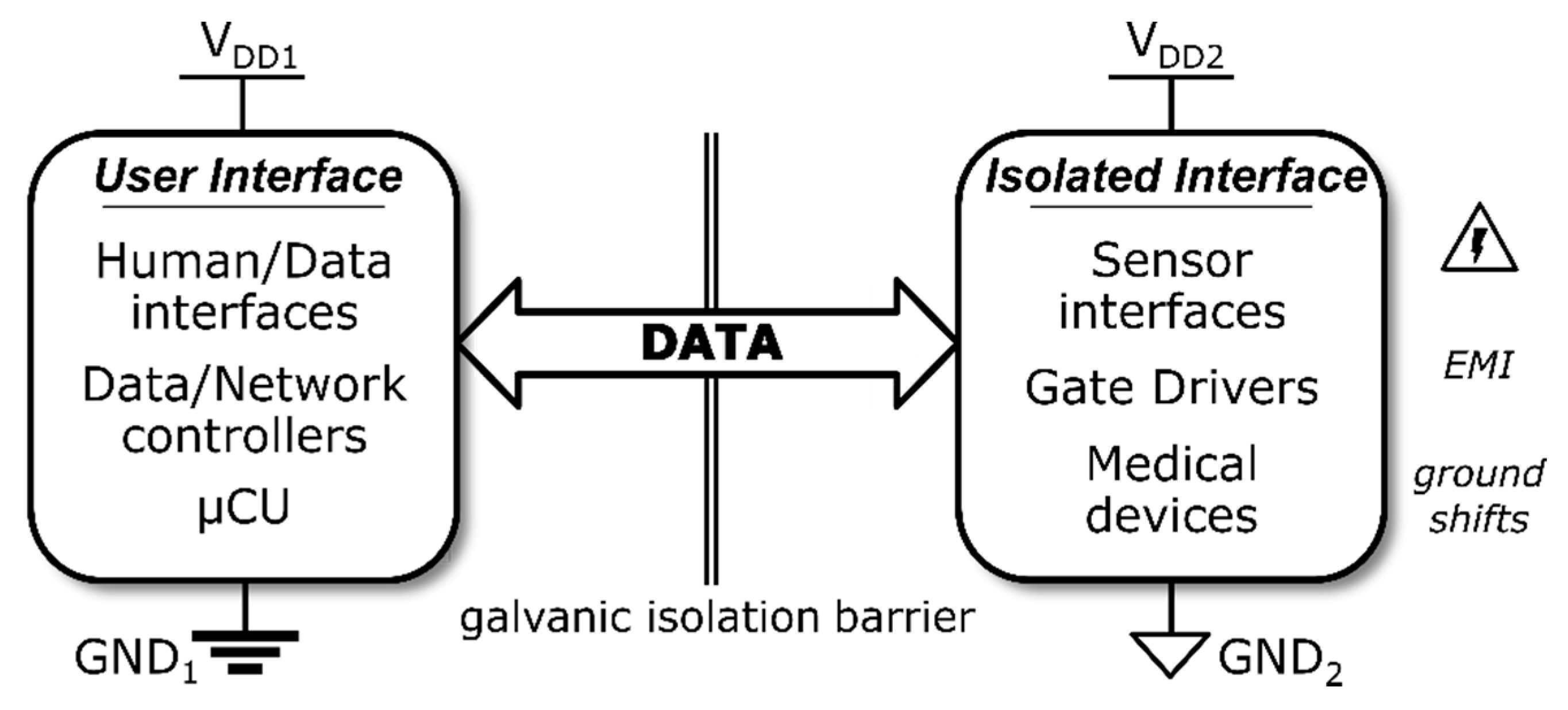
:1. Introduction
2. Technologies for Chip-Scale Galvanic Isolators
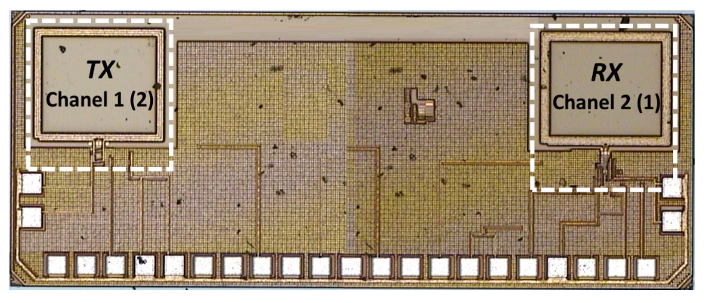
3. Fabrication Technology and System Description
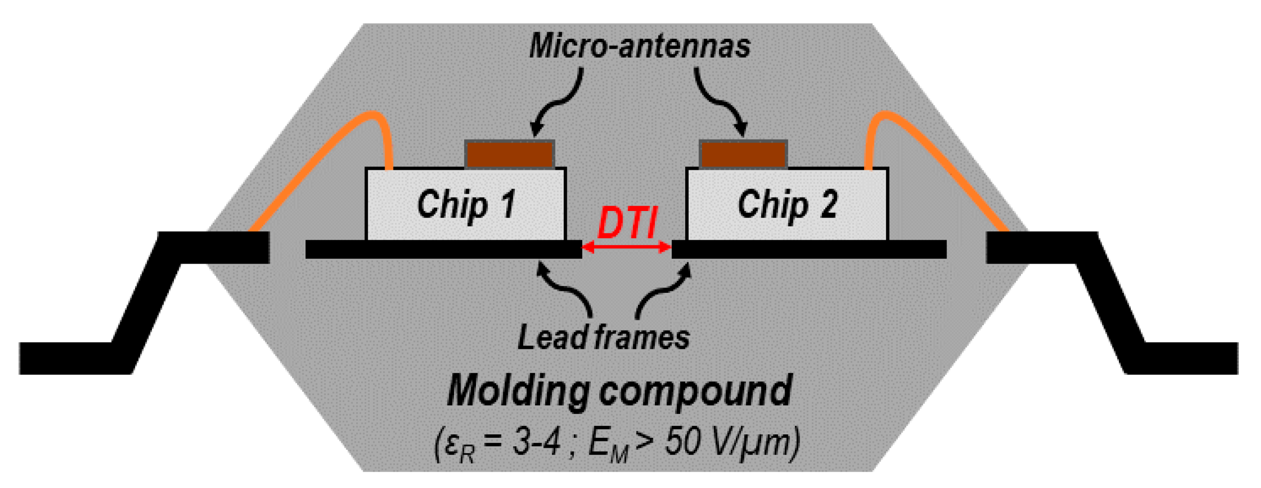
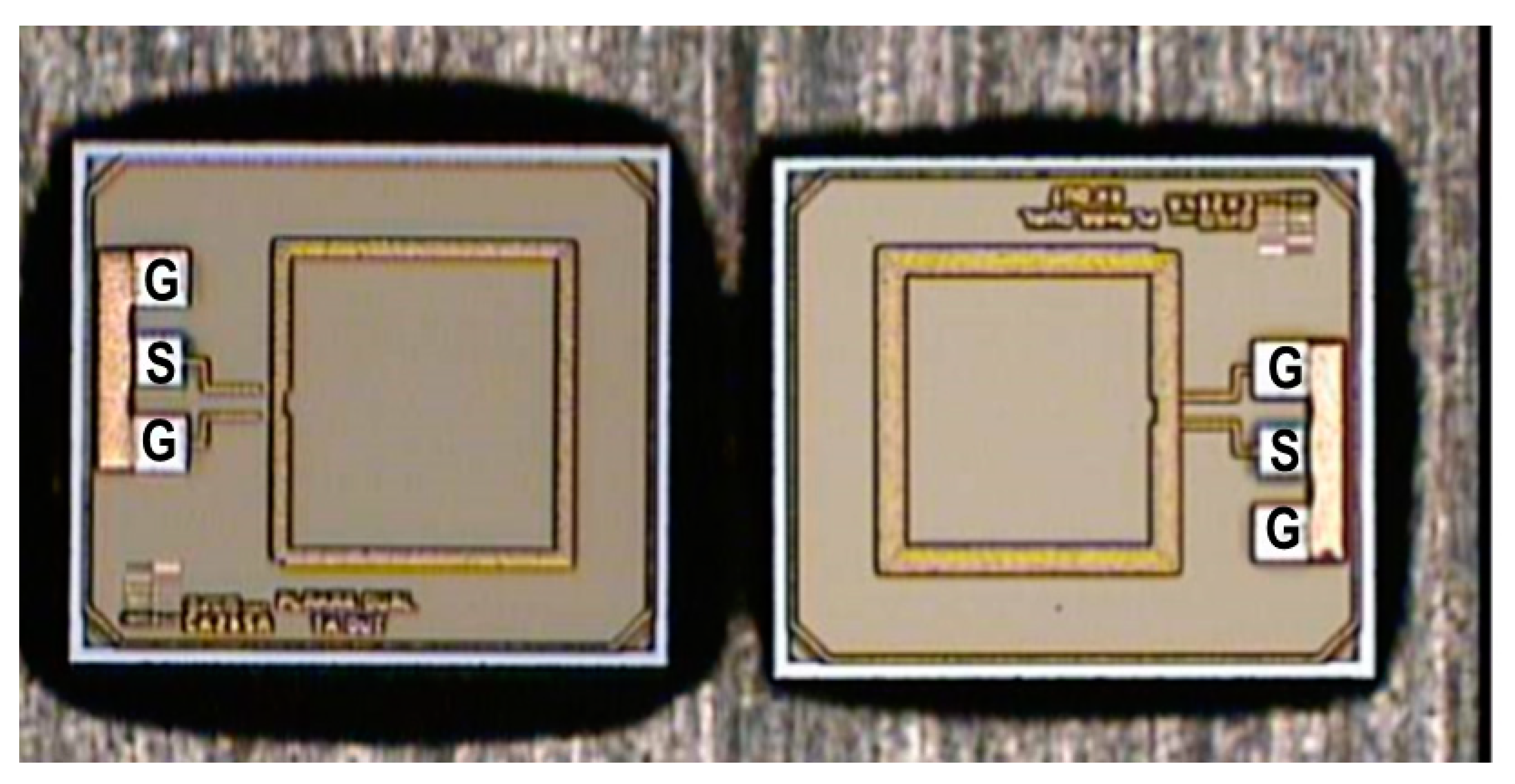
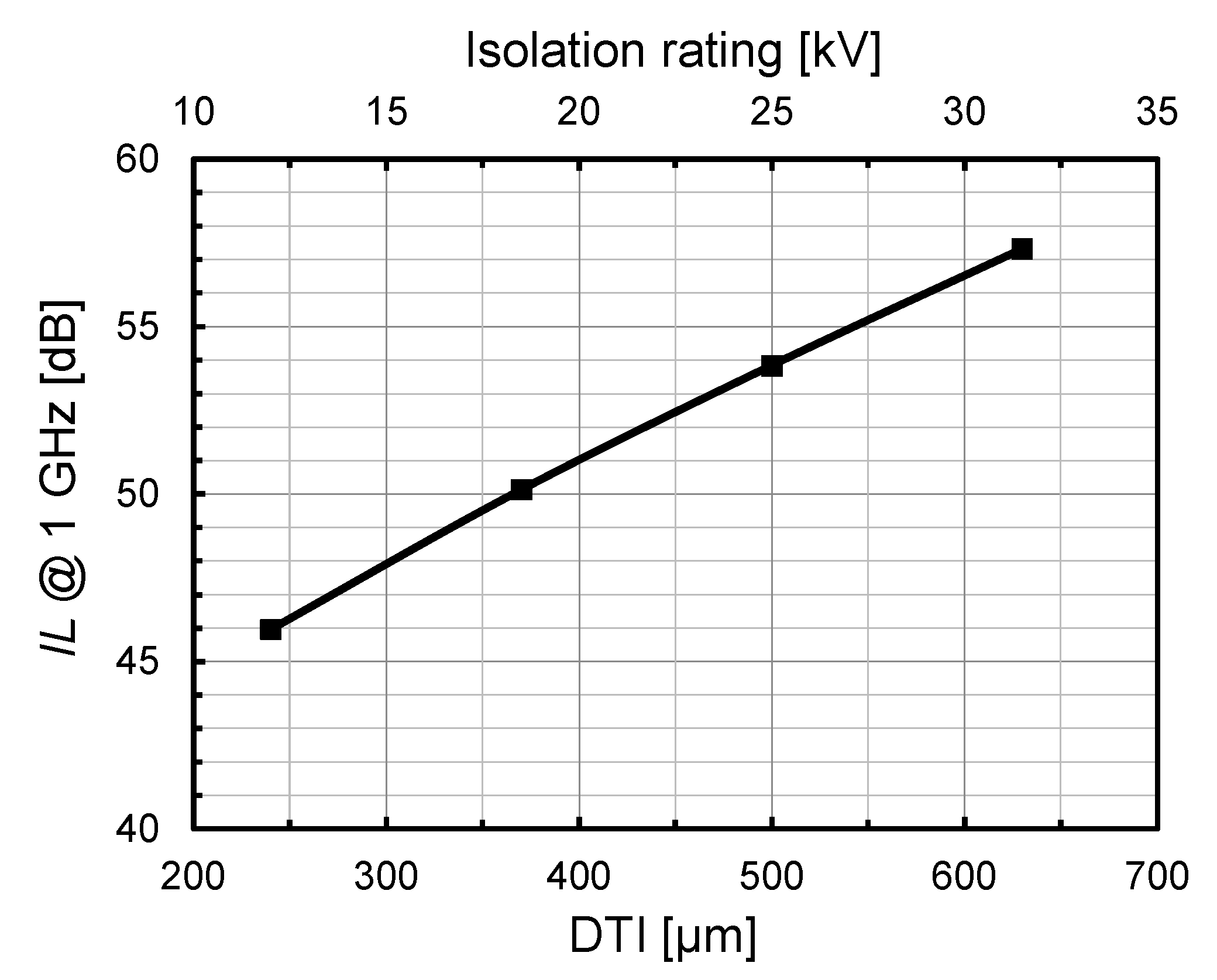
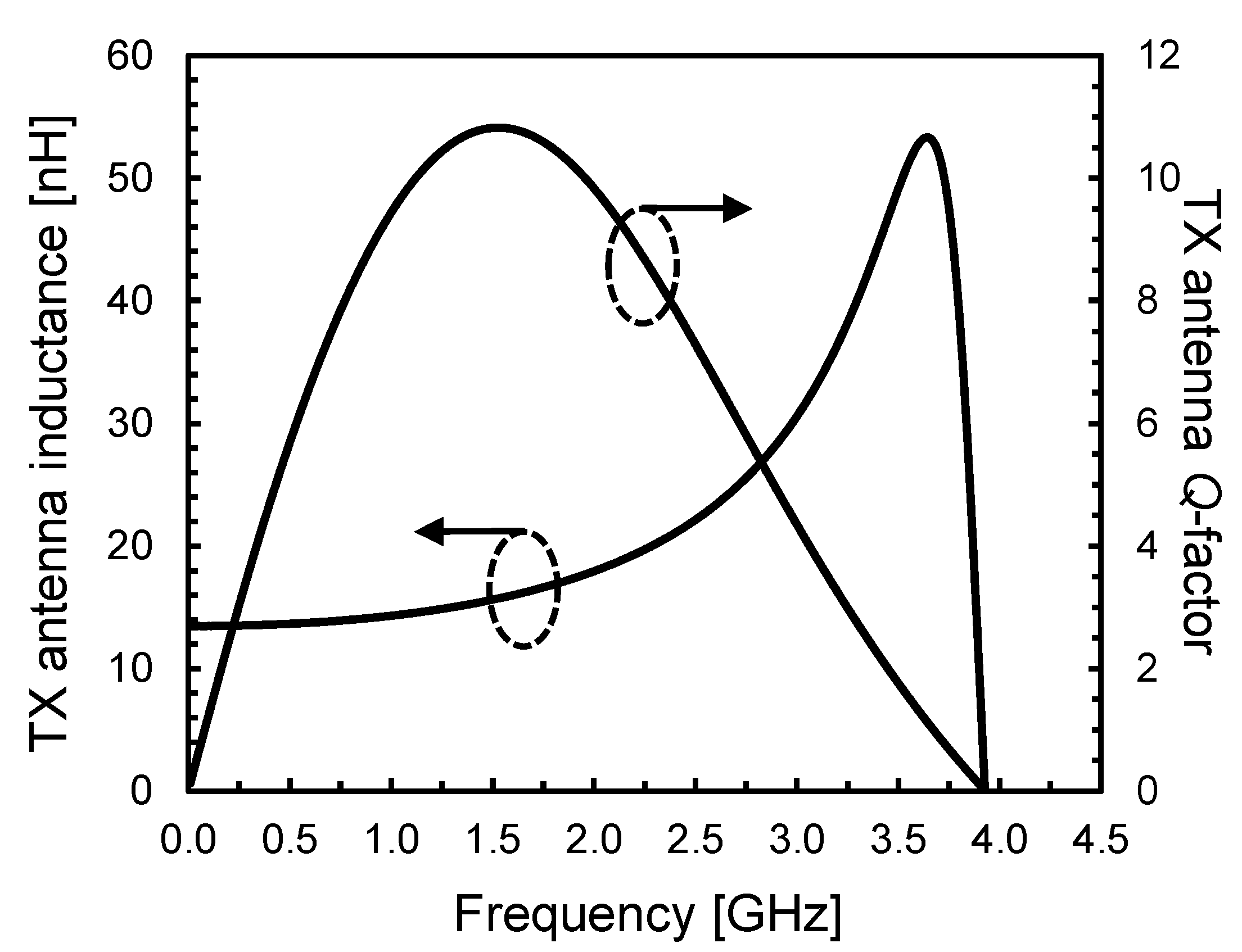
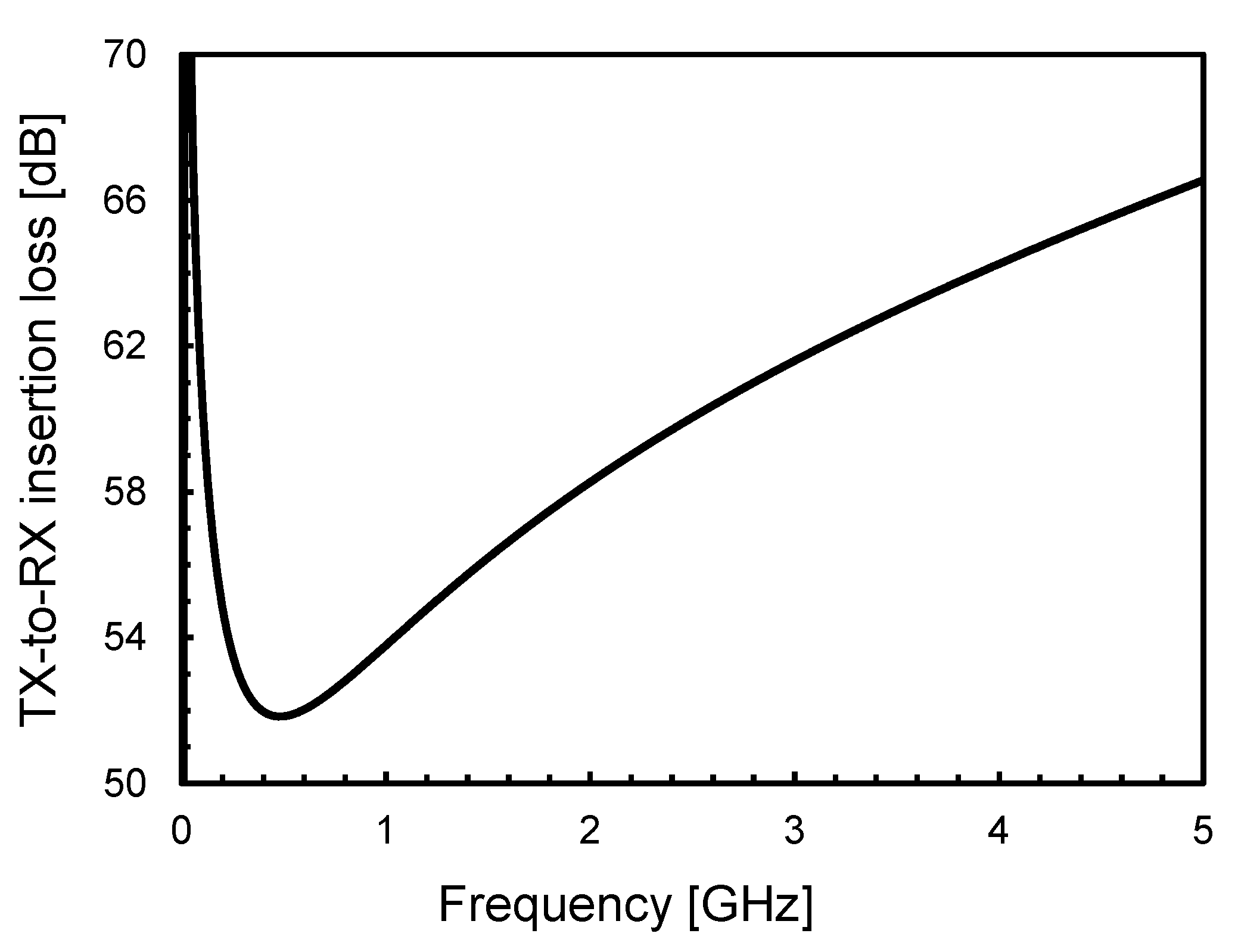
3.1. On-Chip Micro-Antennas
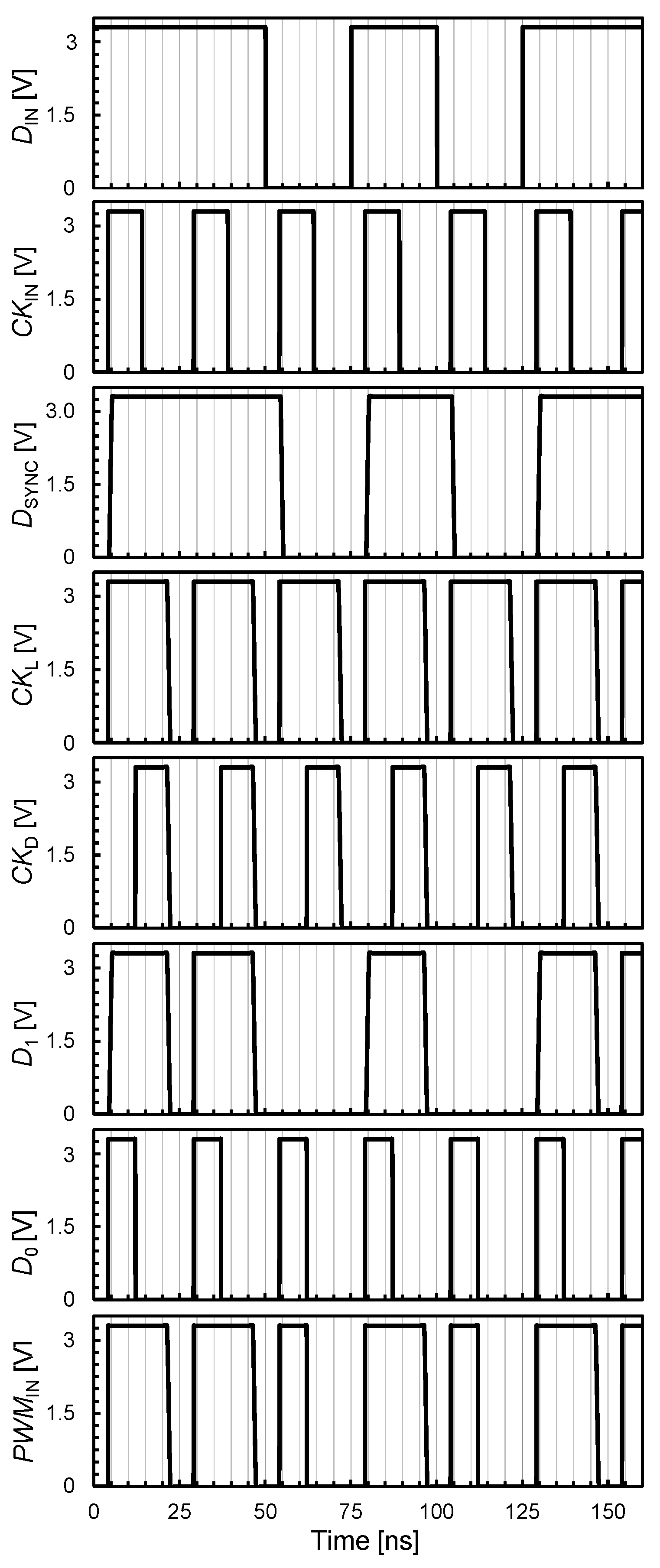
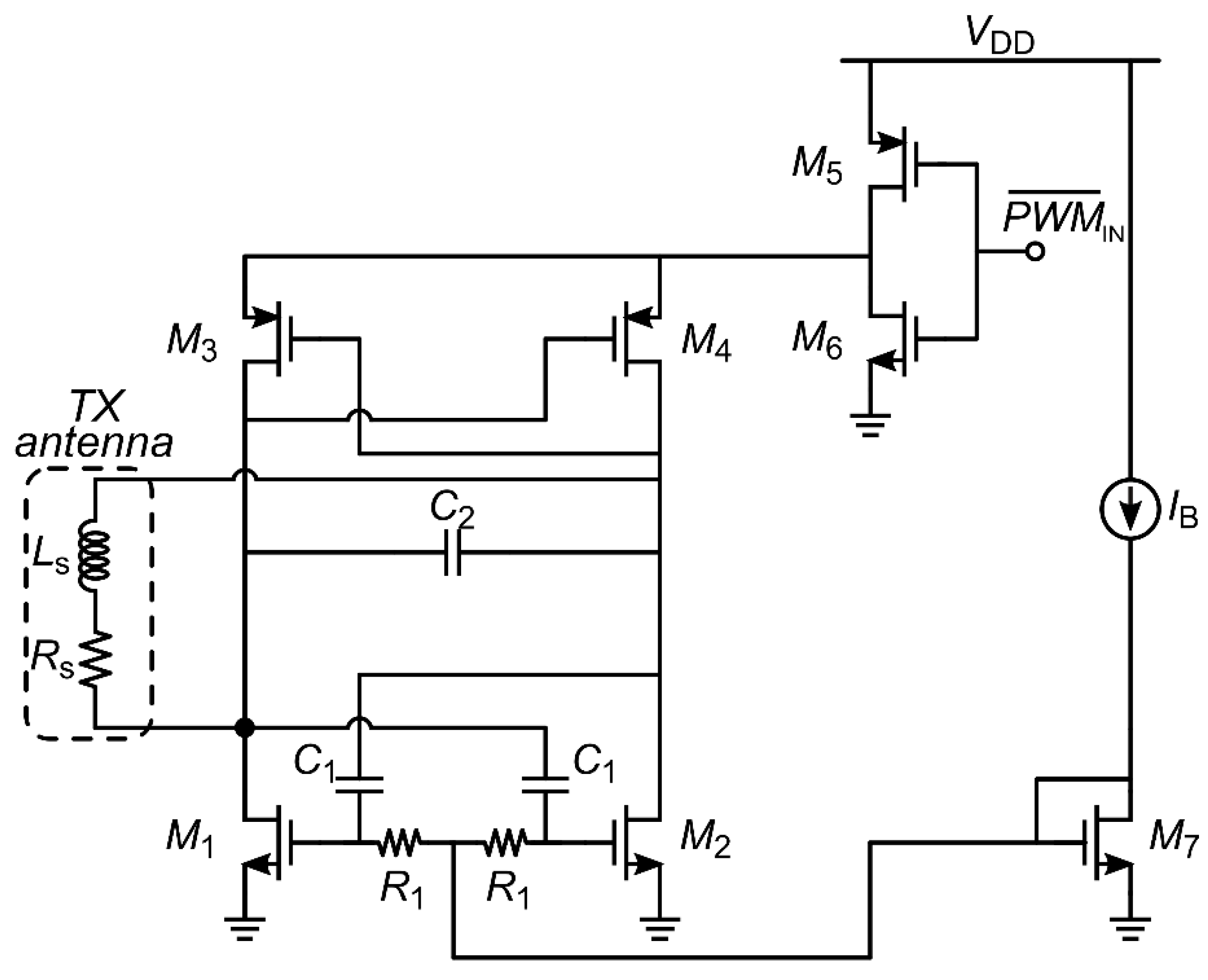
3.2. TX Front-End
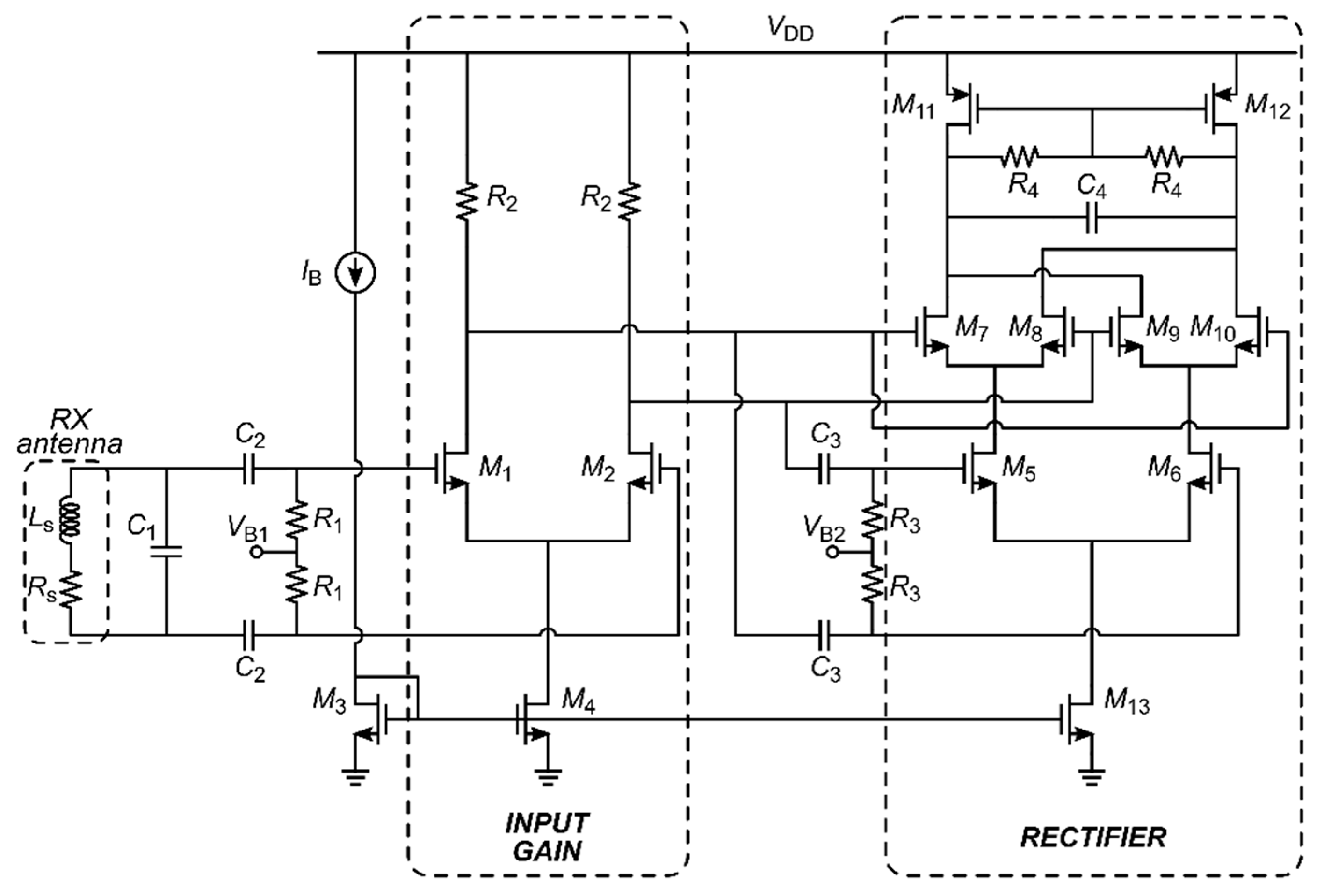
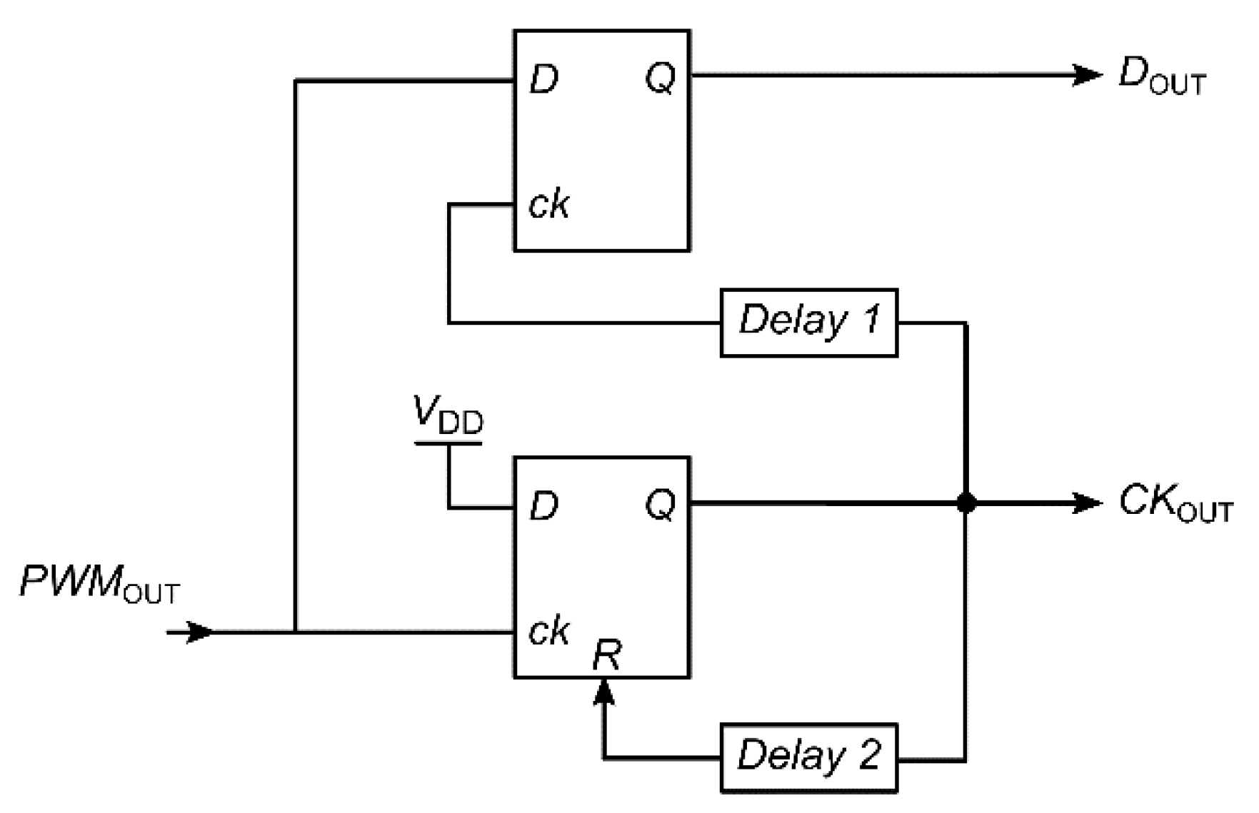
3.3. RX Front-End
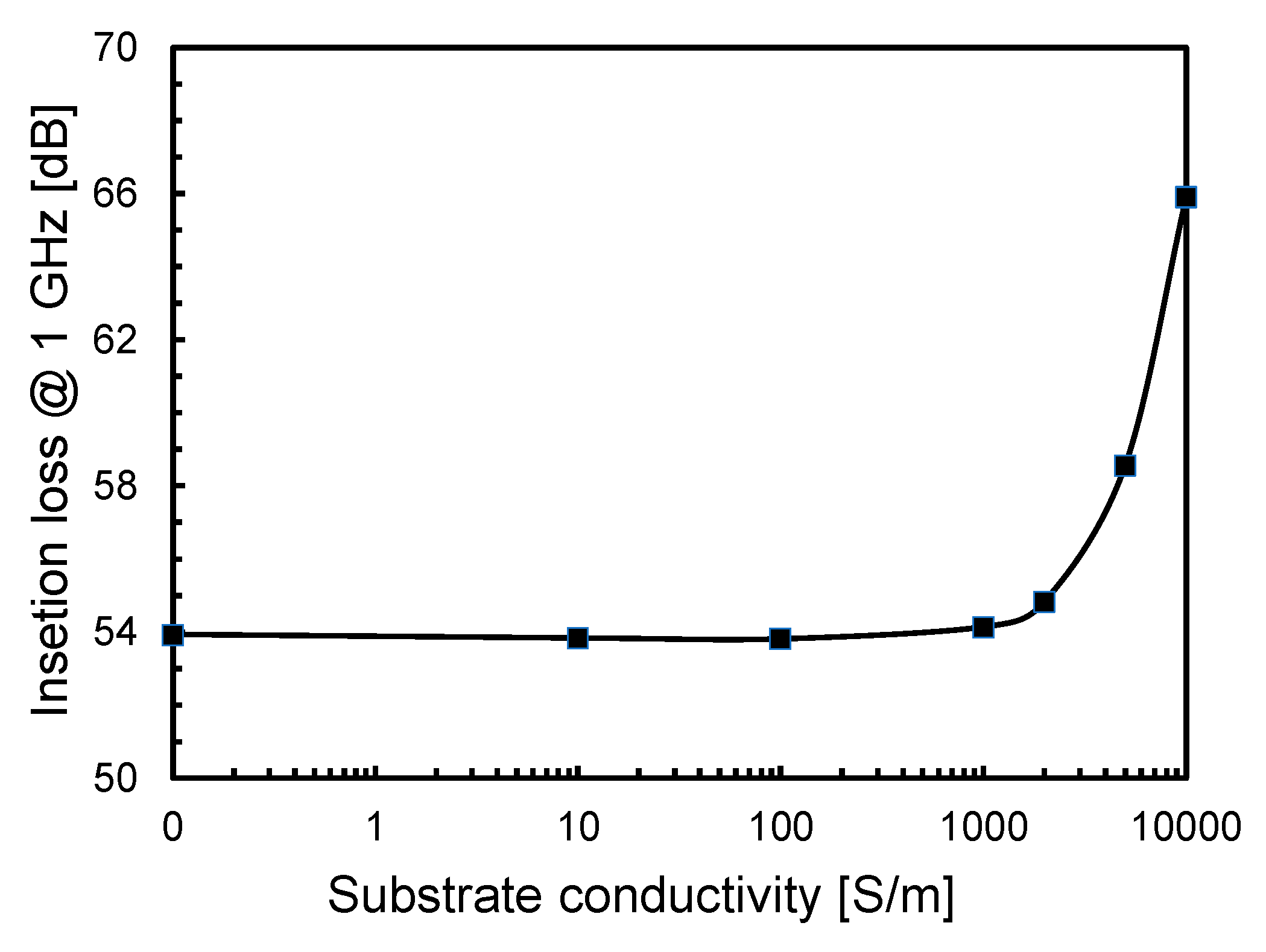
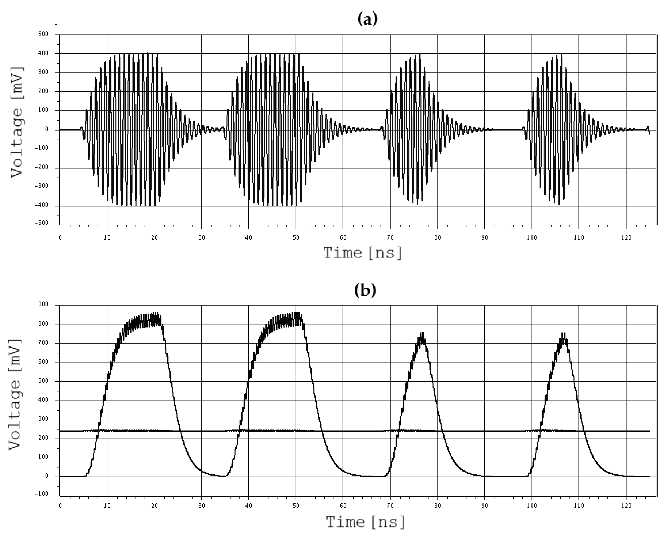
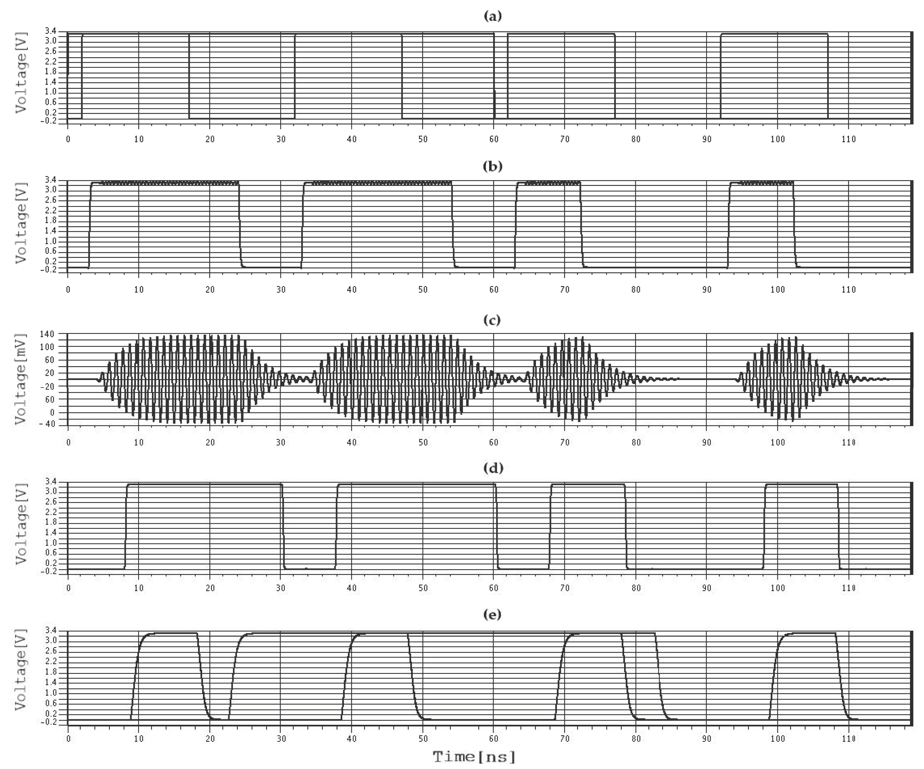
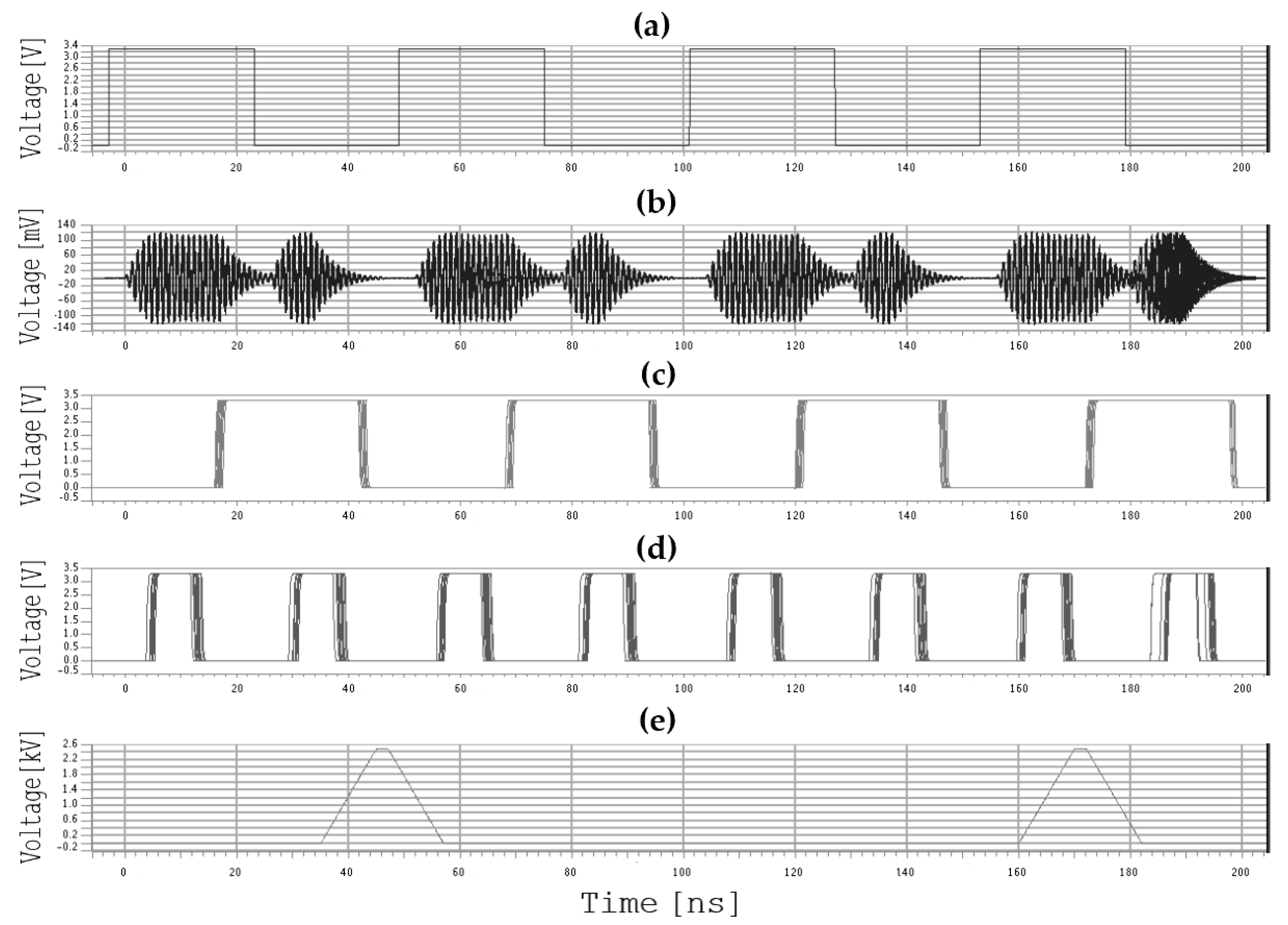
4. Experimental Results
5. Conclusions
Author Contributions
Funding
Acknowledgments
Conflicts of Interest
References
- Devices-Magnetic, D.V.S. DIN VDE Semiconductor Devices-Magnetic and Capacitive Coupler for Basic and Reinforced Isolation; VDE Verlag VDE V 0884-11: Berlin, Germany, 1 January 2017. [Google Scholar]
- Ragonese, E.; Parisi, A.; Spina, N.; Palmisano, G. Reinforced Galvanic Isolation: Integrated Approaches to Go Beyond. In Applications in Electronics Pervading Industry, Environment and Society ApplePies 2019 Lecture Notes in Electrical Engineering; Springer International Publishing: Cham, Switzerland, 2020; Volume 627, pp. 277–283. [Google Scholar]
- Palumbo, V.; Ghidini, G.; Carollo, E.; Toia, F. Integrated Transformer. U.S. Patent App. 14733009, 8 June 2015. [Google Scholar]
- Mahalingam, P.; Guiling, D.; Lee, S. Manufacturing challenges and method of fabrication of on-chip capacitive digital isolators. In Proceedings of the 2007 International Symposium on Semiconductor Manufacturing, Santa Clara, CA, USA, 15–17 October 2007; pp. 1–4. [Google Scholar]
- Krone, A.; Tuttle, T.; Scott, J.; Hein, J.; Dupuis, T.; Sooch, N. A CMOS direct access arrangement using digital capacitive isolation. In Proceedings of the 2001 IEEE International Solid-State Circuits Conference. Digest of Technical Papers, San Francisco, CA, USA, 7 February 2001; pp. 300–301. [Google Scholar]
- Moghe, Y.; Terry, A.; Luzon, D. Monolithic 2.5kV RMS, 1.8V–3.3V dual-channel 640Mbps digital isolator in 0.5μm SOS. In Proceedings of the 2012 IEEE International SOI Conference (SOI), NAPA, CA, USA, 1–4 October 2012; pp. 1–2. [Google Scholar]
- Kaeriyama, S.; Uchida, S.; Furumiya, M.; Okada, M.; Maeda, T.; Mizuno, M. A 2.5 kV isolation 35 kV/us CMR 250 Mbps digital isolator in standard CMOS with a small transformer driving technique. IEEE J. Solid-State Circuits 2012, 47, 435–443. [Google Scholar] [CrossRef]
- Spina, N.; Fiore, V.; Lombardo, P.; Ragonese, E.; Palmisano, G. Current-reuse transformer coupled oscillators with output power combining for galvanically isolated power transfer systems. IEEE Trans. Circuits Syst. I Reg. Pap. 2015, 62, 2940–2948. [Google Scholar] [CrossRef]
- Lombardo, P.; Fiore, V.; Ragonese, E.; Palmisano, G. A fully-integrated half-duplex data/power transfer system with up to 40Mbps data rate, 23mW output power and on-chip 5kV galvanic isolation. In Proceedings of the 2016 IEEE International Solid-State Circuits Conference (ISSCC): Digest of Technical Papers, San Francisco, CA, USA, 31 January–4 February 2016; pp. 300–301. [Google Scholar]
- Greco, N.; Spina, N.; Fiore, V.; Ragonese, E.; Palmisano, G. A galvanically isolated dc-dc converter based on current-reuse hybrid coupled oscillators. IEEE Trans. Circuits Syst. II Exp. Briefs 2017, 64, 56–60. [Google Scholar] [CrossRef]
- Fiore, V.; Ragonese, E.; Palmisano, G. A fully-integrated watt-level power transfer system with on-chip galvanic isolation in silicon technology. IEEE Trans. Power Electron. 2017, 32, 1984–1995. [Google Scholar] [CrossRef]
- Ragonese, E.; Spina, N.; Castorina, A.; Lombardo, P.; Greco, N.; Parisi, A.; Palmisano, G. A fully integrated galvanically isolated DC-DC converter with data communication. IEEE Trans. Circuits Syst. I Reg. Pap. 2018, 65, 1432–1441. [Google Scholar] [CrossRef]
- Javid, M.; Ptacek, K.; Burton, R.; Kitchen, J. CMOS bi-directional ultra-wideband galvanically isolated die-to-die communication utilizing a double-isolated transformer. In Proceedings of the 2018 IEEE 30th International Symposium on Power Semiconductor Devices and ICs (ISPSD), Chicago, IL, USA, 13–17 May 2018; pp. 88–91. [Google Scholar]
- Texas Instruments. ISO7841x High-Performance, 8000-VPK Reinforced Quad-Channel Digital Isolator. Available online: www.ti.com/lit/gpn/ISO7841 (accessed on 4 June 2020).
- Yun, R.; Sun, J.; Gaalaas, E.; Chen, B. A transformer-based digital isolator with 20kVPK surge capability and >200kV/µS common mode transient immunity. In Proceedings of the 2016 IEEE Symposium on VLSI Circuits (VLSI-Circuits), Honolulu, HI, USA, 15–17 June 2016; pp. 1–2. [Google Scholar]
- Qin, W.; Yang, X.; Ma, S.; Liu, F.; Zhao, Y.; Zhao, T.; Chen, B. An 800 mW fully integrated galvanic isolated power transfer system meeting CISPR 22 Class-B emission levels with 6dB margin. In Proceedings of the 2019 IEEE International Solid-State Circuits Conference-(ISSCC): Digest of Technical Papers, San Francisco, CA, USA, 17–21 February 2019; pp. 246–248. [Google Scholar]
- Spina, N.; Girlando, G.; Smerzi, S.A.; Palmisano, G. Integrated Galvanic Isolator Using Wireless Transmission. U.S. Patent 8364195 B2, 29 January 2013. [Google Scholar]
- Renna, C.M.A.; Scuderi, A.; Magro, C.; Spina, N.; Ragonese, E.; Marano, B.; Palmisano, G. Microstructure Device Comprising a Face to Face electromagnetic Near Field Coupling between Stacked Device Portions and Method of Forming the Device. U.S. Patent 9018730 B2, 28 April 2015. [Google Scholar]
- Uchida, S.; Kaeriyama, S.; Nagase, H.; Takeda, K.; Nakashiba, Y.; Maeda, T.; Ishihara, K. A face-to-face chip stacking 7kV RMS digital isolator for automotive and industrial motor drive applications. In Proceedings of the 2014 IEEE 26th International Symposium on Power Semiconductor Devices & IC’s (ISPSD), Waikoloa, HI, USA, 15–19 June 2014; pp. 442–445. [Google Scholar]
- Paye, J.; Claudi, V.; Stecher, M. High voltage robustness of mold compounds under different environmental conditions. In Proceedings of the 2015 IEEE International Reliability Physics Symposium, Monterey, CA, USA, 19–23 April 2015; pp. CP.5.1–CP.5.6. [Google Scholar]
- Paye, J.; Claudi, V.; Stecher, M. High voltage robustness of mold compounds after different treatments. In Proceedings of the 2016 IEEE Electrical Insulation Conference (EIC), Montreal, QC, USA, 19–22 June 2016; pp. 162–165. [Google Scholar]
- Guo, J.; Tan, T. A broadband and scalable on-chip inductor model appropriate for operation modes of varying substrate resistivities. IEEE Trans. Electron Devices 2007, 54, 3018–3029. [Google Scholar] [CrossRef]
- Biondi, T.; Scuderi, A.; Ragonese, E.; Palmisano, G. Characterization and modeling of silicon integrated spiral inductors for high-frequency applications. Analog Integr. Circuits Signal Process. 2007, 51, 89–100. [Google Scholar] [CrossRef]
- Javid, M.; Burton, R.; Ptacek, K.; Kitchen, J. CMOS integrated galvanically isolated RF chip-to-chip communication utilizing lateral resonant coupling. In Proceedings of the 2017 IEEE Radio Frequency Integrated Circuits Symposium (RFIC) Digest, Honolulu, HI, USA, 4–6 June 2017; pp. 252–255. [Google Scholar]
- Mukherjee, S.; Bhat, A.N.; Shrivastava, K.A.; Bonu, M.; Sutton, B.; Gopinathan, V.; Thiagarajan, G.; Patki, A.; Malakar, J.; Krishnapura, N. A 500Mb/s 200pJ/b die-to-die bidirectional link with 24kV surge isolation and 50kV/µs CMR using resonant inductive coupling in 0.18µm CMOS. In Proceedings of the 2017 IEEE International Solid-State Circuits Conference (ISSCC): Digest of Technical Papers, San Francisco, CA, USA, 5–9 February 2017; pp. 434–435. [Google Scholar]
- Krishnapura, N.; Bhat, A.N.; Mukherjee, S.; Shrivastava, K.A.; Bonu, M. Maximizing the data rate of an inductively coupled chip-to-chip link by resetting the channel state variables. IEEE Trans. Circuits Syst. I Regul. Pap. 2019, 66, 3531–3543. [Google Scholar] [CrossRef]


| Antenna | n | s [μm] | w [μm] | dOUT [μm] |
|---|---|---|---|---|
| TX (chip 1) | 3 | 2.75 | 9.6 | 550/650 |
| RX (chip 2) | 5 | 2.75 | 6 | 550/650 |
| Antenna | L1GHz [nH] | Q1GHz | SRF [GHz] | k1GHz | IL1GHz [dB] | TRX_OC [dB] | TRX_10kΩ [dB] |
|---|---|---|---|---|---|---|---|
| TX (chip 1) | 14.3 | 9.4 | 3.93 | 0.004 | 54 | 25 | 27 |
| RX (chip 2) | 43.8 | 8.2 | 2.25 |
| Parameters | [15] | [19] | [24] | [25] | This Work |
|---|---|---|---|---|---|
| Supply voltage, VDD [V] | 1.7–5.5 | 3.3 | 3.5/5(1) | 1.8 | 3.3 |
| Isolation voltage, VSURGE [kV] | 20 | 7(2) | 3.3(2) | 24 | 25 |
| Carrier frequency, fRF [GHz] | 0.7 | n.a. | 2.8 | 1.3/2 | 1 |
| Modulation | OOK | n.a. | OOK | OOK (edge-triggered) | OOK (PWM) |
| Max data rate, fDMAX [Mb/s] | 1 | 1 | 80 | 500 | 40 |
| No. of channels | 1 | 4 | 1 | 2 | 2 |
| CMTI [kV/µs] | 200 | n.a. | n.a. | 50 | 250 |
| Propagation delay, tp [ns] | 11 | 42 | 17.6 | n.a. | 16–20 |
| Energy per bit, EBIT [nJ/bit] | 4.8(3) | 5.5 | 4.2 | 0.15/0.2(4) | 0.5 |
| IDD per channel, IDD_CH [mA] | 2.8(3) | 1.65 | 96 | 0.4/0.6(4) | 6.5 |
| Isolation coupling | Polyimide transformer | Face-to-face stacked antennas | Lateral | Coplanar antennas | Coplanar antennas |
| Silicon technology | 0.18-µm CMOS | 0.25-μm SOI BiCDMOS | 0.25-µm BCD | 0.18-µm CMOS | 0.35-µm CMOS |
| Si area per channel, ACH [mm2] | n.a. | n.a. | 0.94 | 7(5) | 3.8/0.9(6) |
| Assembling/Package | Standard | Stacked chips with DAF(7) | Standard | Standard | Standard |
| FoM1 (8) | 130 | − | − | n.a. | 2404 |
| FoM2 (9) | 286 | − | − | 6000 | 11682 |
| FoM3 (10) | 26 | − | − | − | 730 |
© 2020 by the authors. Licensee MDPI, Basel, Switzerland. This article is an open access article distributed under the terms and conditions of the Creative Commons Attribution (CC BY) license (http://creativecommons.org/licenses/by/4.0/).
Share and Cite
Ragonese, E.; Spina, N.; Parisi, A.; Palmisano, G. A CMOS Data Transfer System Based on Planar RF Coupling for Reinforced Galvanic Isolation with 25-kV Surge Voltage and 250-kV/µs CMTI. Electronics 2020, 9, 943. https://doi.org/10.3390/electronics9060943
Ragonese E, Spina N, Parisi A, Palmisano G. A CMOS Data Transfer System Based on Planar RF Coupling for Reinforced Galvanic Isolation with 25-kV Surge Voltage and 250-kV/µs CMTI. Electronics. 2020; 9(6):943. https://doi.org/10.3390/electronics9060943
Chicago/Turabian StyleRagonese, Egidio, Nunzio Spina, Alessandro Parisi, and Giuseppe Palmisano. 2020. "A CMOS Data Transfer System Based on Planar RF Coupling for Reinforced Galvanic Isolation with 25-kV Surge Voltage and 250-kV/µs CMTI" Electronics 9, no. 6: 943. https://doi.org/10.3390/electronics9060943
APA StyleRagonese, E., Spina, N., Parisi, A., & Palmisano, G. (2020). A CMOS Data Transfer System Based on Planar RF Coupling for Reinforced Galvanic Isolation with 25-kV Surge Voltage and 250-kV/µs CMTI. Electronics, 9(6), 943. https://doi.org/10.3390/electronics9060943