Power Density Maximization in Medium Frequency Transformers by Using Their Maximum Flux Density for DC–DC Converters

 ,
,
Abstract

1. Introduction
Contributions From This Work.
2. Medium-Frequency Transformer Design Procedure
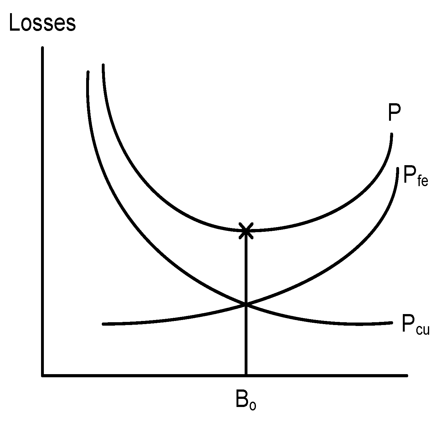
2.1. Transformer Design
2.2. Transformer Design at 75% and 100% of Bmax
| = vacuum permeability | = isolation distance |
| = insulation distance between the layers of the primary | = turns per layer |
| = insulation distance between the layers of the secondary | = winding height |
| = number of layers in the primary | = thickness of the primary |
| = number of layers in the secondary | = thickness of the secondary |
| = mean length of the isolation distance | = penetration ratio of the primary, |
| = mean length turns of primary portion | = penetration ratio of the primary, |
| = mean length turns of secondary portion | where is the skin depth |
3. MTF Laboratory Prototypes
3.1. Transformer Calculation
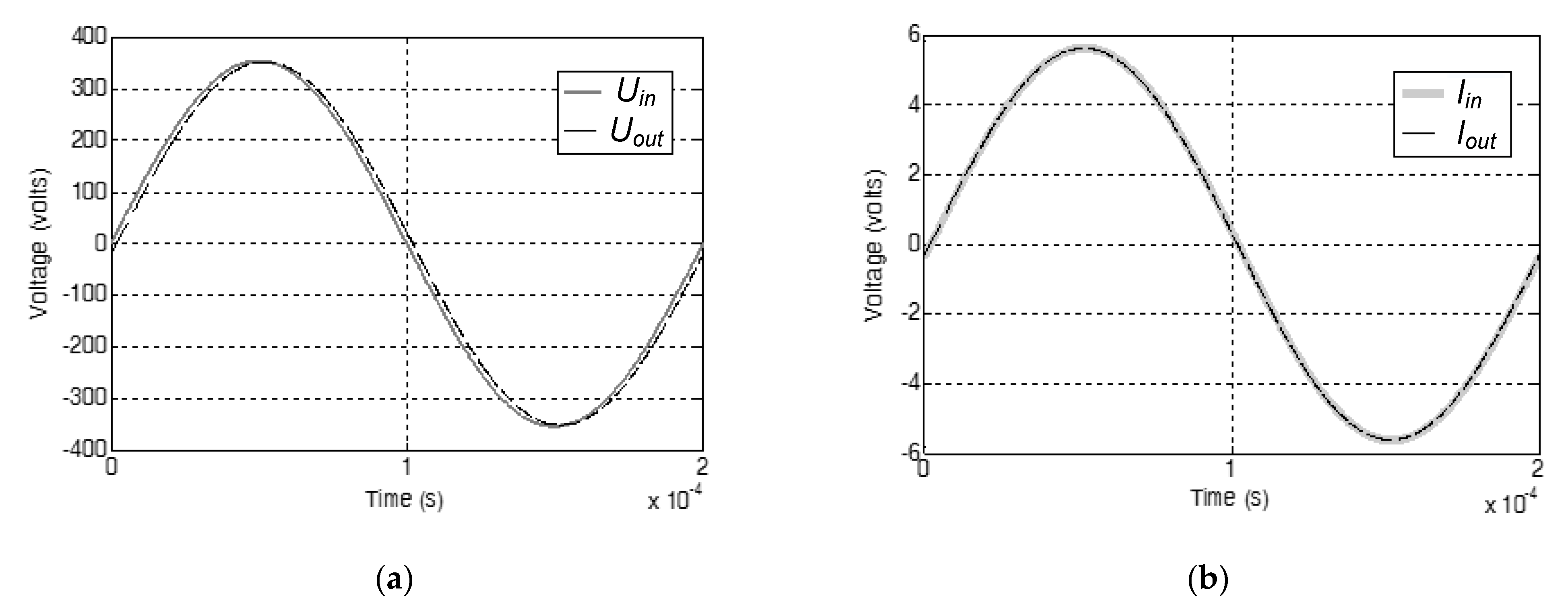
3.2. Simulation
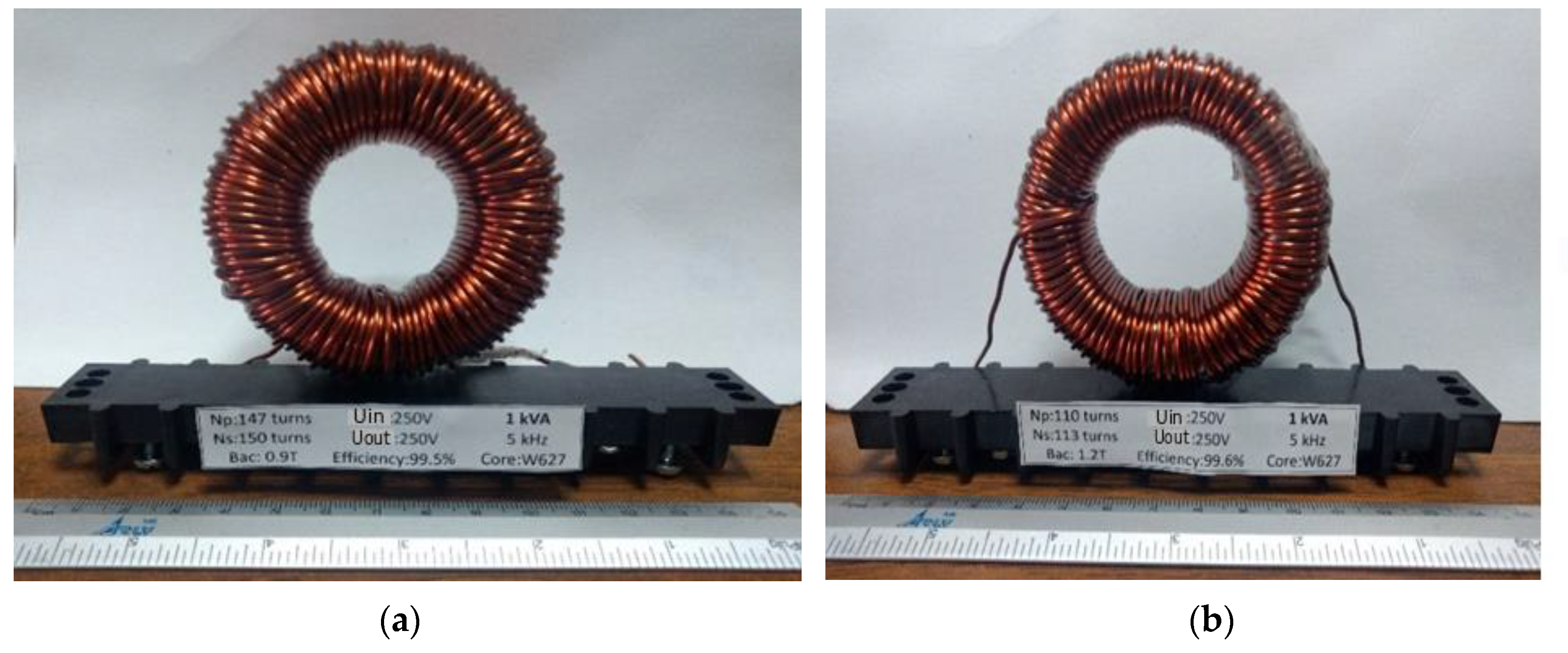
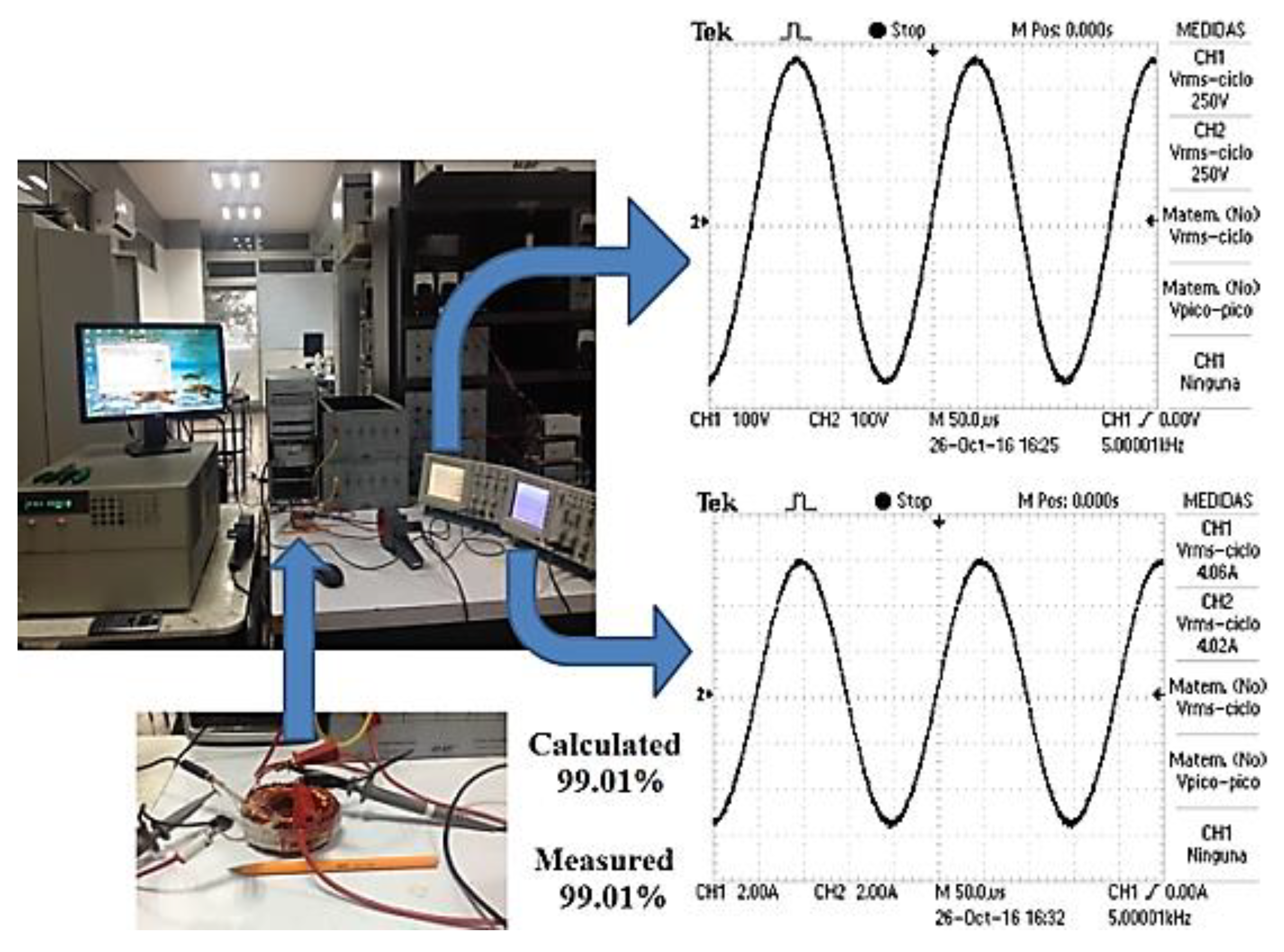
3.3. MFT Prototypes
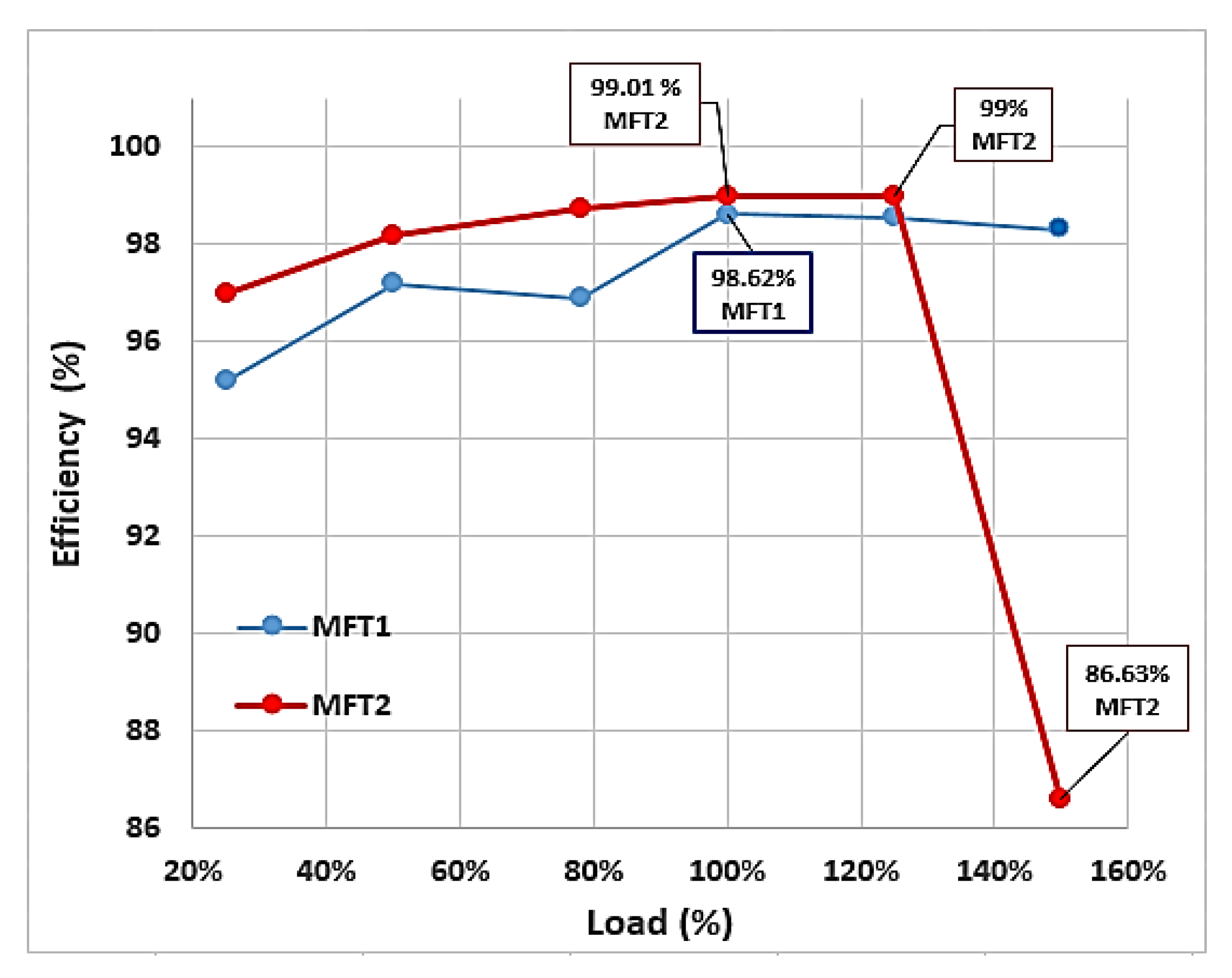
4. Discussion
5. Conclusions
Author Contributions
Funding
Acknowledgments
Conflicts of Interest
References
- Bediaga, A.; Villar, I.; Rujas, A.; Mir, L.; Rufer, A. Multiobjective Optimization of Medium-Frequency Transformers for Isolated Soft-Switching Converters Using a Genetic Algorithm. IEEE Trans. Power Electron. 2017, 32, 2995–3006. [Google Scholar] [CrossRef]
- Ruiz, R.D.; Venegas, R.V.; Anaya, R.A.; Moreno, G.E.; Rodríguez, R.J. Design and prototyping medium-frequency transformers featuring a nanocrystalline core for DC-DC converter. Energy 2018, 11, 2081. [Google Scholar] [CrossRef]
- Krishnamoorthy, H.; Daniel, M.; Ramos, J.; Enjeti, P.; Liu, L.; Aeloiza, E. Isolated AC-DC converter using medium frequency transformer for off-shore wind turbine DC collection grid. IEEE Trans. Ind. Electron. 2017, 64, 8939–8947. [Google Scholar] [CrossRef]
- Leib, M.; Ortiz, G.; Kolar, W. Design and experimental analysis of a medium-frequency transformer for solid-state transformer applications. IEEE J. Emerg. Sel. Top. Pow. Electron. 2017, 5, 110–123. [Google Scholar] [CrossRef]
- Bahmani, M.A.; Thiringer, T.; Kharezy, M. Design methodology and optimization of a medium-frequency transformer for high-power DC-DC applications. IEEE Trans. Ind. Electron. 2016, 52, 4225–4233. [Google Scholar] [CrossRef]
- Huang, P.; Mao, C.; Wang, D.; Wang, L.; Duan, Y.; Qiu, J.; Xu, G.; Cai, H. Optimal design and implementation of high-voltage high-power silicon steel core medium frequency transformer. IEEE Trans. Ind. Electron. 2017, 64, 4391–4401. [Google Scholar] [CrossRef]
- Ozturk, S.; Canver, M.; Cadirci, I.; Ermis, M. All SiC grid-connected PV supply with HF link MPPT converter: system design methodology and development of a 20 kHz, 25 kVA prototype. Electronics 2018, 7, 85. [Google Scholar] [CrossRef]
- Ruiz, D.; Ortíz, J.; Venegas, V.; Moreno, E.; Granados, D.; Rodríguez, J. Nanocrystalline and silicon steel medium frequency transformer applied to dc-dc converters: analysis and experimental comparison. Energies 2019, 12. [Google Scholar] [CrossRef]
- Harischandrappa, N.; Bhat, A.K. A 10 kW ZVS integrated boost dual three-phase bridge DC-DC resonant converter for a linear generator-based wave-energy system: design and simulation. Electronics 2019, 8, 115. [Google Scholar] [CrossRef]
- She, X.; Huang, Q.; Burgos, R. Review of solid-state transformer technologies and their application in power distribution system. IEEE J. Emerg. Sel. Top. Pow. Electron. 2013, 1, 186–198. [Google Scholar] [CrossRef]
- Wang, Y.; Ni, F.; Lee, T. Hybrid modulation of bidirectional three-phase dual-active-bridge DC converters for electric vehicles. Energy 2016, 9, 492. [Google Scholar] [CrossRef]
- Hosseinzadeh, M.; Rajaci, F. Robust optimal power management system for a hybrid AC/DC micro-grid. IEEE Trans. Sust. Energ. 2015, 6, 675–687. [Google Scholar] [CrossRef]
- Lee, J.H.; Lee, S.H.; Sul, S.K. Variable-speed engine generator with supercapacitor: isolated power generation system and fuel efficiency. IEEE Trans. Ind. Applic. 2009, 45, 2130–2135. [Google Scholar] [CrossRef]
- Hilzinger, R.; Rodewald, W. Magnetic Materials, 1st ed.; Publicis MCD Werbeagentur GmbH, Vaccumschmelze GmbH & Co. KG: Hanau, Germany, 2013; pp. 280–290. [Google Scholar]
- Sixdenier, F.; Morand, J.; Salvado, A.; Bergogne, D. Statistical study of nanocrystalline alloy cut cores from two different manufacturers. IEEE Trans. Magn. 2014, 50, 2003604. [Google Scholar] [CrossRef]
- Chailloux, T.; Raulet, M.; Martin, C.; Joubert, C.; Sixdenier, F.; Morel, L. Magnetic behavior representation taking into account the temperature of a magnetic nanocrystalline material. IEEE Trans. Magn. 2012, 48, 455–458. [Google Scholar] [CrossRef]
- Prochazca, R.; Hlavacek, J.; Draxler, K. Magnetic circuit of a high-voltage transformer up to 10 kHz. IEEE Trans. Magn. 2015, 51. [Google Scholar] [CrossRef]
- Kauder, T.; Hameyer, K. Performance factor comparison of nanocrystalline, amorphous, and crystalline soft magnetic materials for medium-frequency applications. IEEE Trans. Magn. 2017, 53, 8401504. [Google Scholar] [CrossRef]
- Roch, A.; Leferink, F. nanocrystalline core material for high-performance common mode inductors. IEEE Trans. Electromagn. Compat. 2012, 54, 785–791. [Google Scholar] [CrossRef]
- She, X.; Yu, X. Design and demonstration of a 3.6-kV-120-V/10-kVA solid-state transformer for smart grid application. IEEE Trans. Pow. Electron. 2014, 29, 3982–3996. [Google Scholar] [CrossRef]
- Hurley, W.; Wolfle, W. Transformer and Inductor for Power Electronics: Theory, Design and Applications; John Wiley & Sons Ltd: West Sussex, UK, 2013; Volume 1, ISBN 9781119950578. [Google Scholar]
- McLyman, C.W. Transformer and Inductor Design Handbook; CRC Press: New York, NY, USA, 2011. [Google Scholar]
- Bahmani, M.A.; Thiringer, T. Accurate evaluation of leakage inductance in high frequency transformer using an improved frequency dependent expression. IEEE Trans. Pow. Electron. 2015, 30, 5738–5745. [Google Scholar] [CrossRef]
- Hurley, W.; Wilcox, D. Calculation of leakage inductance in transformer windings. IEEE Trans. Pow. Electron. 1994, 9, 121–126. [Google Scholar] [CrossRef]
- Soltau, N.; Eggers, D.; Hameyer, K.; Doncker, R. Iron losses in a medium-frequency transformer operated in a high-power DC-DC converter. IEEE Trans. Magn. 2014, 50. [Google Scholar] [CrossRef]


| Design Data | |
|---|---|
| Uin | 1000 V |
| Uout | 1000 V |
| f | 5000 Hz |
| Iout | 10 A |
| Bac | 0.9 T |
| Np | 278 |
| Ns | 282 |
| Pcu | 87 W |
| Pfe | 1.51 W |
| Ptot | 88.51 W |
| Efficiency | 99.1% |
| Wa | 50.26 cm2 |
| Ac | 2 cm2 |
| Ap | 100.53 cm2 |
| Required Data | |
|---|---|
| Uin | 1000 V |
| Uout | 1000 V |
| Winding 1 parameters | |
| Iout | 10 A |
| Bac | 0.9 T |
| Np | 278 |
| Winding 2 parameters | |
| Pcu | 87 W |
| Pfe | 1.51 W |
| Ptot | 88.51 W |
| Magnetization resistance and inductance | |
| Wa | 50.26 cm2 |
| Ac | 2 cm2 |
| Voltages and Currents | |
|---|---|
| Uin (RMS) | 1000 V |
| Uout (RMS) | 990.1 V |
| Iin (RMS) | 9.913 A |
| Iout (RMS) | 9.901 A |
| Efficiency | 98.90% |
| Design Data | |
|---|---|
| Uin | 1000 V |
| Uout | 1000 V |
| f | 5000 Hz |
| Iout | 10 A |
| Bac | 1.2 T |
| Np | 209 |
| Ns | 212 |
| Pcu | 65.4 W |
| Pfe | 2.12 W |
| Ptot | 67.52 W |
| Efficiency | 99.3% |
| Wa | 50.26 cm2 |
| Ac | 2 cm2 |
| Ap | 100.53 cm2 |
| Design Data | ||
|---|---|---|
| Parameter | MFT1 | MFT2 |
| Uin | 250 V | 250 V |
| Uout | 250 V | 250 V |
| F | 5000 Hz | 5000 Hz |
| Iout | 4 A | 4 A |
| Bac | 0.9 T | 1.2 T |
| Np | 147 | 110 |
| Ns | 150 | 112 |
| Pcu | 11.74 W | 8.78 W |
| Pfe | 0.62 W | 1.12 W |
| Ptot | 12.36 W | 9.89 W |
| Efficiency | 98.80% | 99.01% |
| Wa | 19.63 cm2 | 19.63 cm2 |
| Ac | 0.95 cm2 | 0.95 cm2 |
| Ap | 18.65 cm4 | 18.65 cm4 |
| Required Data | MFT1 | MFT2 |
|---|---|---|
| Pout (VA) | 1000 | 1000 |
| f (Hz) | 5000 | 5000 |
| Winding 1 parameters | ||
| Uin (RMS) | 250 | 250 |
| R1 (Ω) | 0.2729 | 0.2042 |
| Ld1 (H) | 0.000031 | 0.0000238 |
| Winding 2 parameters | ||
| Uout (RMS) | 250 | 250 |
| R2 (Ω) | 0.2729 | 0.2042 |
| Ld2 (H) | 0.000031 | 0.0000238 |
| Magnetization resistance and inductance | ||
| Rm (Ω) | 111270 | 111270 |
| Lm (H) | 0.194 | 0.1087 |
| Voltages and Currents | MFT1 | MFT2 |
|---|---|---|
| Uin (RMS) | 250 V | 250 V |
| Uout (RMS) | 247.7 V | 248.25 V |
| Iin (RMS) | 3.966 A | 3.98 A |
| Iout (RMS) | 3.963 A | 3.97 A |
| Efficiency | 99% | 99.05% |
| Measurement | MFT1 | MFT2 |
|---|---|---|
| Input power | 1002 W | 1015 W |
| Output power | 1005.96 W | 1005 W |
| Core losses | 1.15 W | 2.02 W |
| Winding losses | 12.84 W | 7.97 W |
| Total losses | 14.04 W | 10 W |
| Uin | Uout | Iin | Iout | Efficiency | |
|---|---|---|---|---|---|
| Nominal voltage (Unom) | 250 V | 250 V | 4.06 A | 4.02 A | 99.01% |
| 12% above Unom | 280 V | 279 V | 4.55 A | 4.48 A | 98.11% |
| 13% above Unom | 283 V | 282 V | 4.84 A | 4.56 A | 93.88% |
| 15% above Unom | 287 V | 286 V | 4.65 A | 4.65 A | 86.93% |
| MFT1 | MFT2 | |||
|---|---|---|---|---|
| THDI | THDV | THDI | THDV | |
| Nominal voltage (Unom) | 0.55% | 0.52% | 0.54% | 0.52% |
| 12% above Unom | 0.53% | 0.54% | 2.23% | 0.70% |
| 13% above Unom | 0.54% | 0.53% | 4.68% | 1.77% |
| 15% above Unom | 0.53% | 0.53% | 8.82% | 3.86% |
| Design Flux Density | Reference | Core | Efficiency | Power Density |
|---|---|---|---|---|
| 1.2 T | This proposal | nanocrystalline | > 99% | 15.62 kW/l |
| 0.9 T 0.9 T 0.35 T 0.5 T | Ruiz 2018, [2] Bahmani 2016, [5] Asier 2017, [1] Huang 2017, [6] | nanocrystalline nanocrystalline ferrite silicon steel | > 99% > 99% > 99% > 99% | 15.01 kW/l 11.5 kW/l 9.25 kW/l 2.96 kW/l |
| 0.6 T | Harish 2017, [3] | silicon steel | > 99% | 1.29 kW/l |
| Transformer | Power | Frequency | Volume | Weight | Power Density | Cost |
|---|---|---|---|---|---|---|
| Conventional | 1 kVA | 50 Hz/60 Hz | 783 cm3 | 7 kg | 1.28 kW/l | 241.18 USD |
| MFT | 1 kVA | 5 kHz | 64 cm3 | 0.25 kg | 15.62 kW/l | 67.87 USD |
© 2020 by the authors. Licensee MDPI, Basel, Switzerland. This article is an open access article distributed under the terms and conditions of the Creative Commons Attribution (CC BY) license (http://creativecommons.org/licenses/by/4.0/).
Share and Cite
Ruiz-Robles, D.; Moreno-Goytia, E.L.; Venegas-Rebollar, V.; Salgado-Herrera, N.M. Power Density Maximization in Medium Frequency Transformers by Using Their Maximum Flux Density for DC–DC Converters. Electronics 2020, 9, 470. https://doi.org/10.3390/electronics9030470
Ruiz-Robles D, Moreno-Goytia EL, Venegas-Rebollar V, Salgado-Herrera NM. Power Density Maximization in Medium Frequency Transformers by Using Their Maximum Flux Density for DC–DC Converters. Electronics. 2020; 9(3):470. https://doi.org/10.3390/electronics9030470
Chicago/Turabian StyleRuiz-Robles, Dante, Edgar L. Moreno-Goytia, Vicente Venegas-Rebollar, and Nadia M. Salgado-Herrera. 2020. "Power Density Maximization in Medium Frequency Transformers by Using Their Maximum Flux Density for DC–DC Converters" Electronics 9, no. 3: 470. https://doi.org/10.3390/electronics9030470
APA StyleRuiz-Robles, D., Moreno-Goytia, E. L., Venegas-Rebollar, V., & Salgado-Herrera, N. M. (2020). Power Density Maximization in Medium Frequency Transformers by Using Their Maximum Flux Density for DC–DC Converters. Electronics, 9(3), 470. https://doi.org/10.3390/electronics9030470