1. Introduction
Memristor is a nonlinear two-terminal electrical component that completes a theoretical quartet of fundamental electrical components by relating electric charge and magnetic flux linkage. It was postulated by Leon Chua [
1] and later generalized to a broader class of dynamical circuit-theoretic concept to a memristive system [
2]. Memristor creates immense attention after the seminal paper published by
hp in 2008, which reveals that the electrical resistance of the device is not constant, but depends on the history of previous inputs [
3]. It is considered as one of the most promising element in emerging memory sector [
4,
5,
6] and neural applications [
7,
8], due to its propitious attributes under DC or AC excitation and miniature nanoscale physical dimension along with synapse alike operation. Recently, numerous research activities are ongoing on binary and multistate phenomena in generic and extended memristors [
9,
10,
11,
12,
13,
14,
15,
16] which could lead to another stage of technical innovation in the memristor area. Nonlinear dynamics theory, and circuit and system theoretic concepts can be devoted to explaining the principle of the multistate memristors [
9].
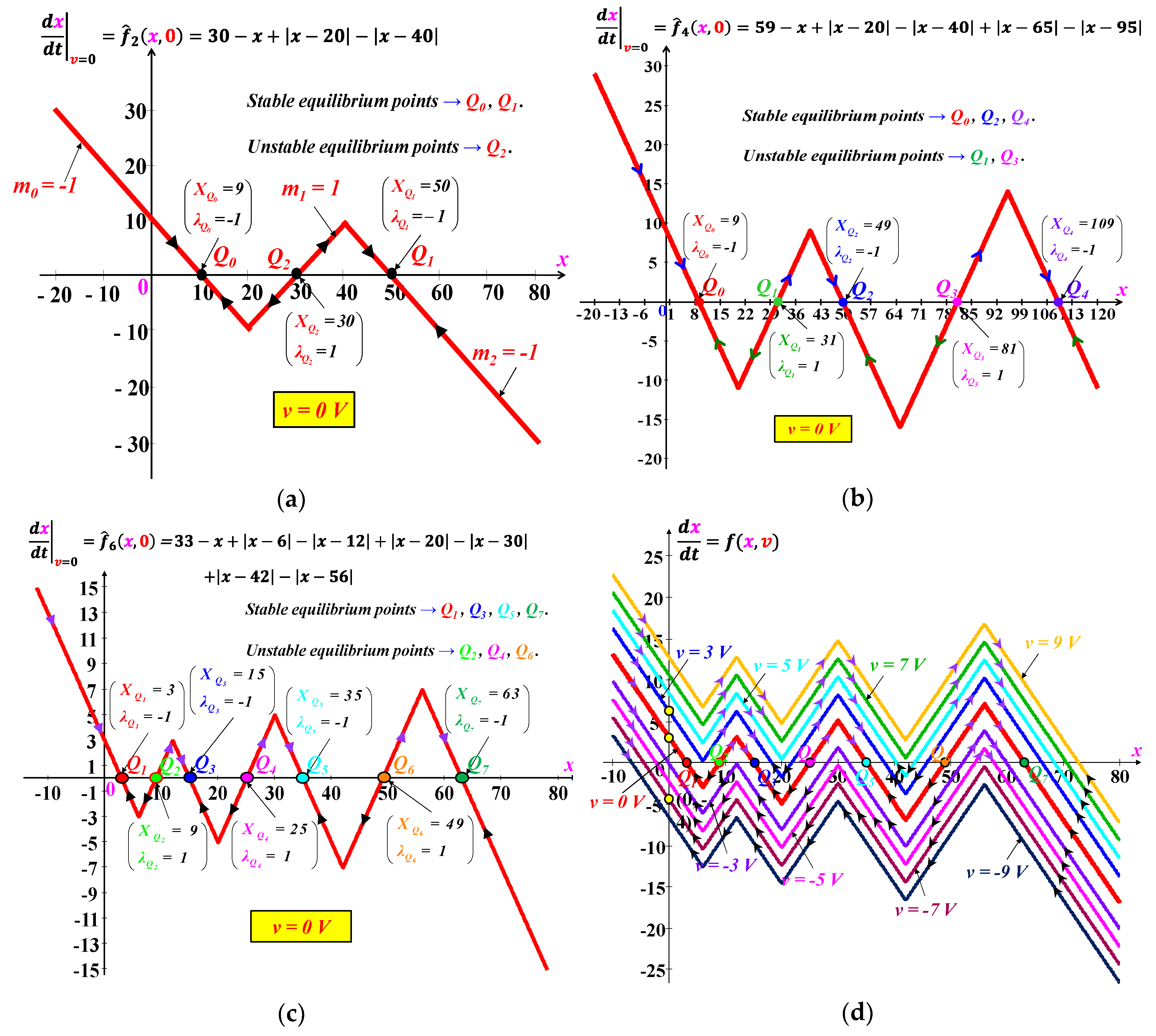
This review paper presents an in-depth and rigorous nonlinear and bifurcation analysis, switching kinetics, and physical realization of the three members of Chua corsage memristor (
CCM) family. The CC memristors exhibit a highly nonlinear DC
V-I curves, due to the presence of a higher degree of versatility in its dynamic route map (
DRM) which has multiple stable equilibrium points. The DC
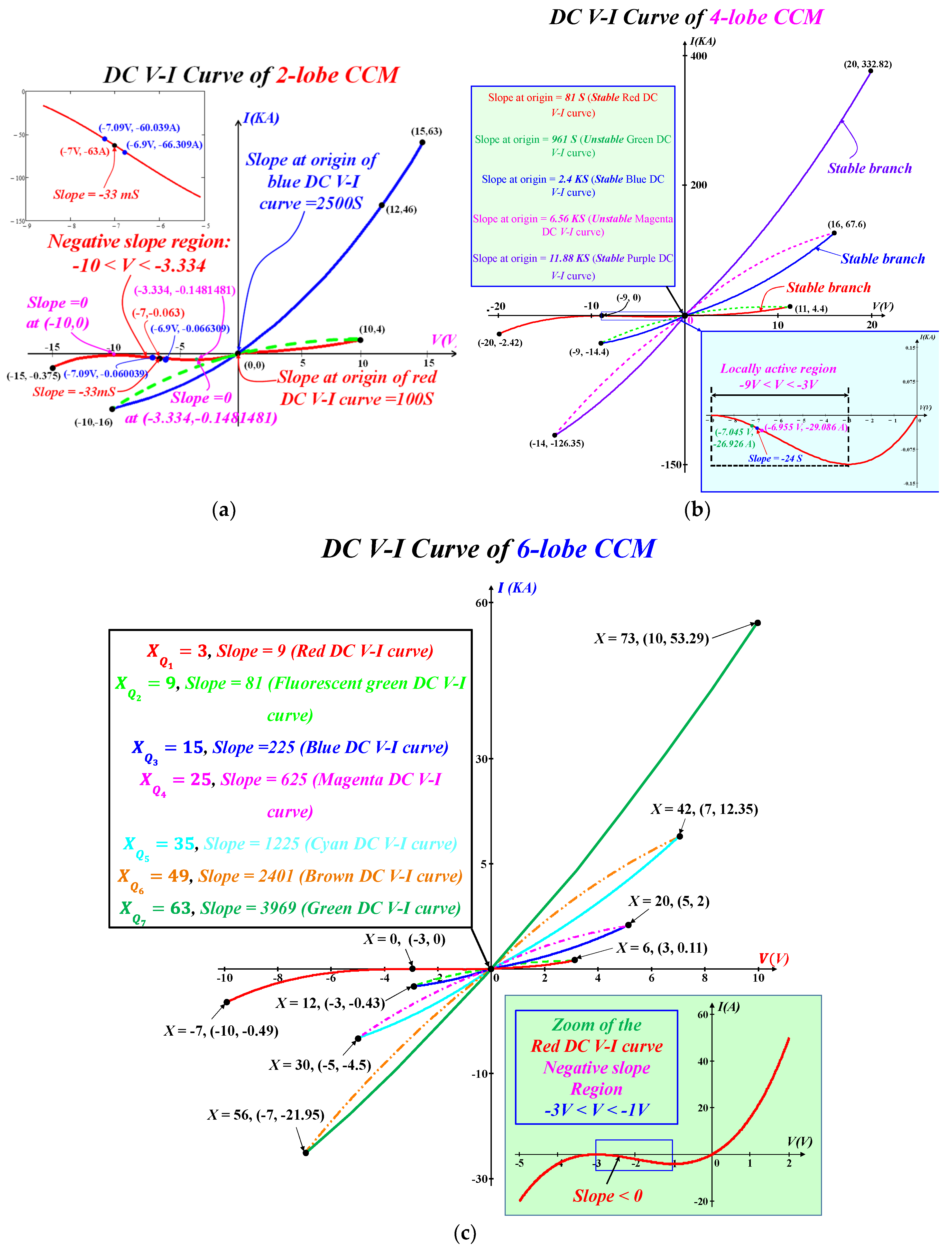
V-I curves of
CCMs are contiguous compared to most published highly-nonlinear DC
V-I curves which have several
disconnected branches. The DC
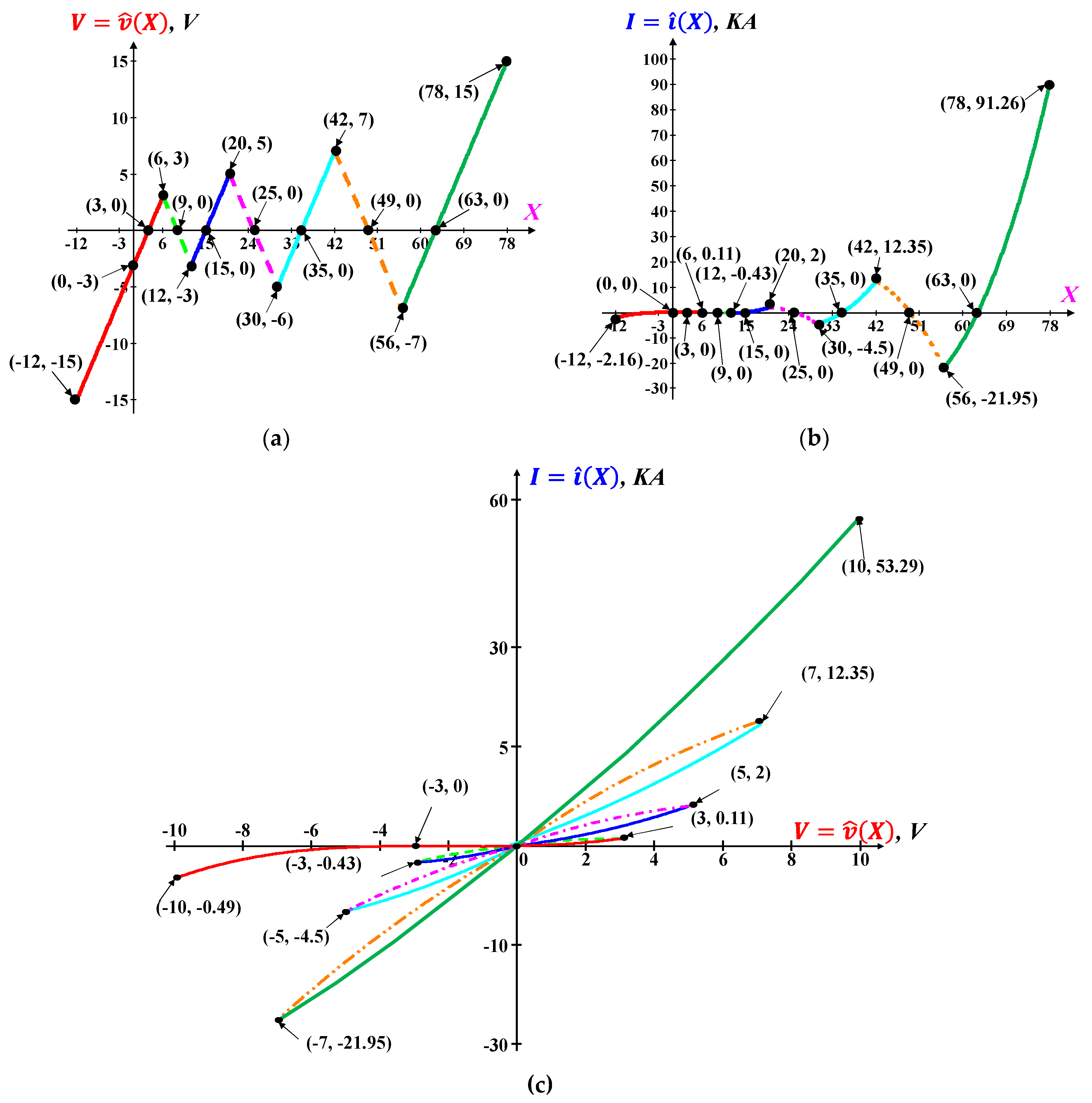
V-I curves of
CCMs have an explicit analytical equation with its parametric representation that rarely happens. In addition, each member of
CCM family exhibits a negative slope region on its DC
V-I curve which give rise to complexity by exploiting local activity; and
complex phenomenon and information processing might emerge over the parameter ranges of
CCMs either operating on or near the neighborhood of its
edge of chaos domain [
12,
13,
14,
15,
16].
The locally active
CCM family exhibit asymptotical stability via the supercritical Hopf bifurcation [
13,
14,
15,
16]. The state altering of
CCMs follows the nonlinear dynamic route of a chosen initial state
xn(0) and repeats until the state reaches in a particularly stable state which is termed as an “attractor”. The state space of
CCMs contain various attractors, and each attractor has its own basin of attraction [
13,
14,
15,
16]. The equilibrium state of these type of memristors moves by the amount of time integral of applied inputs or noises that are applied at a stable equilibrium state. However, the state of
CCMs returns back to its original equilibrium state (attractor), unless the state moves beyond the boundary of the current basin of attraction [
13,
14,
15,
16]. Therefore, it can be utilized as a robust bistable or multistate memory device. However, the CC memristors lost a part of previous programming history in this procedure, where such a phenomenon is known as “local fading memory” in bistable and multistate memory devices [
10,
11].
Another feature of the multistate
CCMs is the alteration of stable equilibria which requires an input pulse, either a sufficiently large amplitude with a short pulse width or a minimum pulse amplitude with lengthy pulse width. When input pulse is applied, the corsage memristors switch from one stable equilibrium state to another stable state by converging into the basin of the new stable attractor. The resistances or conductances of each attractor, i.e., stable equilibrium states, are distinguishably different from each other [
12,
13,
14,
15,
16]. The successful alteration of the stable equilibria of
CCMs is dependent on applied input pulse amplitude and width along with the initial condition. Trajectory movement of the altering equilibria can be demonstrated by computing the time-dependent exponential state trajectories
xn(
t) for an individual straight-line segment of PWL
DRM where time
t = tfn is required for the trajectory of
xn(
t) to move from any initial point to the end point of that particular segment.
In spite of theoretical insights, concepts from circuit and system theory, and techniques from nonlinear dynamics theory are devoted in this review to investigate the physical realization of the real emulator circuits for
CCM family. To design a physical emulator circuit for
CCMs, at least a passive nonlinear-resistive two-port along with a dynamic first-order one-port is required [
10,
11,
12]. The passive nonlinear-resistive two-port is designed with two parallel connected Graetz bridges [
17]. In contrast, the dynamic first-order one-port is designed with a capacitor in parallel with an
active and locally active resistor where the resistor must exhibit the behavioral attributes of piecewise linear
CCMs.
Rest of the article is organized as follows: Introduction of
CCM family and their nonlinear dynamical attributes are presented in
Section 2, followed by memory state switching kinetics in
Section 3. Local activity and Hopf bifurcation are analyzed in
Section 4, and the physical realization of
CCM emulator is demonstrated in
Section 5.
Section 6 contains the concluding remarks.
3. Switching Kinetics of CCM Family
DC
V-I analysis, in
Figure 3, and
power-off-plot, in
Figure 2, explicitly indicate that the Chua corsage memristors can be used as a binary and multistate memory device at
v = 0
V. Conceptually, the simplest way to switch the memory states of a memory device is to apply a pulse input with an appropriate pulse amplitude
VA, and pulse width Δ
w. For successful switching between the memory states of
CCM, the square pulse should have a minimum pulse width Δ
w for appropriate pulse amplitude,
VA. Any square pulse with less than the minimum pulse width results in switching failure. The switching kinetics of
CCMs can be represented through its
dynamic route map where the solution of each straight-line segments of
DRM is an exponential function of state variable
xn(
t). The complete solution of time-dependent
x(t) is made of a sequence of the exponential waveforms joined at the various breakpoints in the dynamic routes [
12]. Due to complex and diversified dynamic routes with
multiple asymptotically stable equilibrium points, 6-lobe
CCM is chosen to illustrate the successful switching from lower conductance state (resp., higher resistance state) to higher conductance state (resp., lower resistance state) or vice-versa along with switching failure.
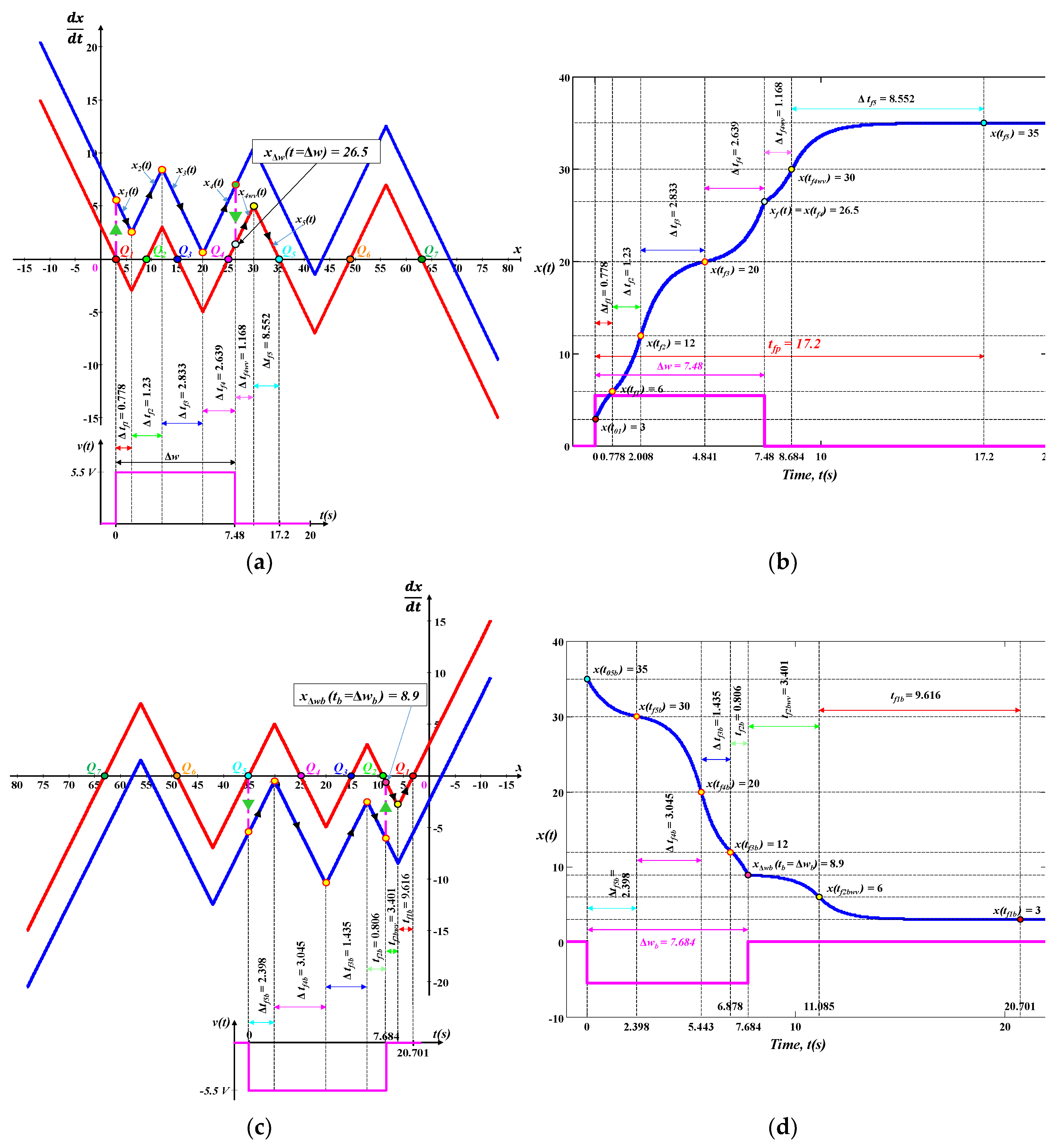
Example 1. Successful switching from lower conductance state Q1 to higher conductance state Q5.
The dynamic route map, in
Figure 4a, shows the example of a successful switching of the 6-lobe
CCM from low conductance state
Q1 to high conductance state
Q5 when a pulse input with an amplitude
VA= 5.5
V, and width Δ
w = 7.48 s is applied. According to Sect. II-A, the applied pulse with
VA = 5.5
V is equivalent to translating the red curve
f(
x, 0) upwards by 5.5 units, as shown by the blue curve
f(
x, 5.5). The dynamic route starting from low conductance state
Q1 (
x = 3) at
t = 0
- would jump abruptly from
Q1 on red curve to a point directly above
Q1 on the blue curve (yellow circle) at
t = 0
+ (shown with upward green arrow) as the pulse input increases from 0
V to 5.5
V. Since the blue curve is located above the
x-axis (where
dx/dt > 0), its motion can only move to the right until time
t = Δ
w. At
t = Δ
w, the square pulse returns to zero and the point
xΔw(
t = Δ
w) = 26.5 (shown with green circle) on the blue curve (
f(
x, 5.5)) reverts back abruptly to the same point on the red curve (shown with light cyan circle followed by a downward green arrowhead). On red curve (
f(
x, 0)), state variable
x(
t) =
xΔw(
t) diverges away from unstable equilibrium point
Q4 (
x = 25) and must continue to move rightward along the dynamical movement of
DRM (i.e.,
dx/dt > 0) until it converges to the low-resistance memory state
Q5 (
x = 35), as indicated with black arrowheads in
Figure 4a.
The exponential trajectories of
xn(
t) related to the individual piecewise linear segments are shown in
Figure 4b. The total time period needed for the
x(
t) (
x(
t) is the collective trajectory of all exponential trajectories
xn(
t) that originated from each straight-line segments of
DRM between
Q1 and
Q5.) trajectory to reach to
Q5 from
Q1 is
tfp = 17.2 s, although the applied pulse is removed at t = Δ
w = 7.48 s. This phenomenon illustrates the local fading memory attributes of 6-lobe
CCM, but reveals the opportunity of utilizing it as a multistate memory device.
Example 2. Successful switching from higher conductance state Q5 to lower conductance state Q1.
To switch from high conductance state
Q5 to low conductance state
Q1 of the 6-lobe
CCM, a negative pulse with amplitude
VA = −5.5
V and width Δ
wb = 7.684
s is applied. The dynamic route and the state trajectories
x(t) of switching kinetics from
Q5 to
Q1 are shown in
Figure 4c,d, respectively.
Figure 4c shows that the dynamic route starting from
Q5 (
x = 35) on red curve jumps abruptly downward by −5.5 units at
t = 0
+, as shown with blue curve
f(
x, −5.5). The state variable
x(
t) then moves towards the lower conductance state
Q1 as
dx/dt < 0. At
tb = Δ
wb, when the negative input is removed, state variable
xΔwb (tb = Δ
wb) = 8.9 on blue curve returns to the exact same position on the red curve and continues to move towards
Q1 (
x = 3) as
dx/dt < 0. The exponential trajectories of
xn(t) from memory state
Q5 to
Q1 is shown in
Figure 4d where the
xn(t) decreases as the time increases and converges to
x(
tf1b) = 3 which is regarded as the
Q1 memory state. The 6-lobe
CCM exhibits dissimilar switching time in spite of similar pulse amplitude and greater pulse width as the switching time from higher to lower conductance states,
tfpb = 20.701 s, is greater than
tf = 17.2 s. This reveals that the
CCM exhibits similar anti-symmetrical switching complication like as other memristive multistate memory devices.
Example 3. Switching failure from lower conductance state Q1 to higher conductance state Q5.
Amplitude
VA and pulse width Δ
w of an applied input pulse plays a crucial role in the switching kinetics of memory states of the 6-lobe
CCM. An inappropriate pulse amplitude or pulse width may result in switching failures which illustrated in
Figure 5. An appropriate pulse amplitude
VA = 5.5
V with a pulse width Δ
w = 7 s is applied to the 6-lobe
CCM to switch the memory state from
Q1 to
Q5.
Figure 5 shows that the exponential trajectories are converging to memory state
Q3 (
x = 15) rather than converging to memory state
Q5 (
x = 35). This switching failure happens as the state variable
x(
t) fails to cover the distance of
x(
t) >
XQ4 = 25 with a pulse width Δ
w = 7 s. Before the removal of input, the trajectories of state variable
x(
t) reaches to a point
xΔw(
t = Δ
w) = 23.812 which lies in the left-hand side of
Q4 (
x = 25), as shown in
Figure 5a. According to
Section 2.1, any point lies in the left-side of
Q4 (
x = 25) should follow the dynamic route
dx/dt < 0 (as shown with black arrowhead in
Figure 2) and converges to equilibrium state
Q3 and in this case, the state variable
x(
t) follows the same route
dx/dt < 0 and converges to
Q3 (
x = 15) rather converging to memory state
Q5 (
x = 35), as shown in
Figure 5b.
To overcome the switching failure problem, this review article includes the universal formulas (For detail derivation and explanation regarding the universal formulas please refer to ref. [
12] and its supplementary materials.) that is required to determine the appropriate pulse amplitude
VA and pulse width Δ
w. To do so, the exponential trajectories of state variable
xn(
t) and the time
tfn that required for the trajectorial movement from any initial point
x(
tin) to the end of straight-line segment of
DRM are computed. The exponential trajectory of state variable
xn(t) of a straight-line segment of the
DRM at an equilibrium point
Qn is determined as
where, n represents the number of equilibrium points and m represents the sign value of the straight-line slope,
and
tin is the initial time of the straight-line segment; whereas,
x(
tin) represents the initial state at
tin. The time (
tfn), that required for the trajectory of
xn(
t) to move from any initial point
x(tin) to the end of the straight-line segment of
DRM, can be defined as
The complete movement of the exponential trajectories of state variable
xn(
t) can be determined by accumulating all the individual exponential trajectories of the straight-line segments of
DRM,
where there trajectories of
xn(
t) only valid over
tin ≤ t < tfn and
p represent the total number of
PWL segments of the
DRM between initial point
x(tin)and final converged equilibrium point
Qn.
The appropriate pulse amplitude
VA is determined as
where
Q(n-1) and
x(
t0(n-1)) represent the immediate before equilibrium point and the initial state of the resultant memory state
Qn.
The pulse width Δ
w is defined as
where
q represents the number of straight-line segments of the
DRM over
x(
tin) ≤
x(
t) ≤
xΔw (
t = Δ
w) and
xΔw is the user-defined state where the applied input is removed. The value of user-defined
xΔw determines whether the alteration of memory states is going to be successful or not. For example, in spite choosing
xΔw (
t = Δ
w) >
X = 25(
Q4) in
Figure 4a, any user-define state value
xΔw (
t = Δ
w) ≤
X = 25(
Q4) results in unsuccessful switching between
Q1 and
Q5 and the resultant exponential trajectory converges to
Q3 memory state, as shown in
Figure 5.
These formulas (Equations (13)–(18)) are universal as they can be applicable to any piecewise linear dynamic routes for any DC or pulse input and with any number of segments. Moreover, the universal formulas in Equations (17) and (18) compute the minimum pulse amplitude and width, which can be used to solve the anti-symmetrical switching complications, in Example 2. Unlike other memristive multistate memory devices which require empirical approach, the CC memristors are defined by universal analytical formulas to determine the appropriate pulse amplitude and width for successful switching from lower conductance state to higher conductance state or vice-versa.
4. Local Activity and Bifurcation Analysis
Local activity principle predicts the presence of
complex phenomena in a nonlinear dynamical system [
23]. Particularly it affirms that a nonlinear circuit made of 2-terminal circuit elements, and/or more complicated 2-terminal devices, can exhibit complex
bifurcation phenomena, such as
oscillation and
chaos, if and only if the circuit contains at least one nonlinear locally-active element. The fundamental deep mathematical theorem given in [
23] allows testing the
locally active phenomenon of a device about some
equilibrium points, i.e.
, DC operating points.
According to the theorem presented in [
23], 2-lobe, 4-lobe and 6-lobe
CCMs are locally active over the interval
−10
V <
V < −3.334
V (in
Figure 2a),
−9
V < V < −3
V (in
Figure 2b), and −3
V < V < −1
V (
Figure 2c), respectively, as the slope at any point
Q over these intervals is negative, i.e.,
Re [
Y(
iω)] < 0 at
Q and
ω = 0 (DC input), which satisfies the locally active criterion of Re [
Z(
iω)]
< 0, or Re [
Y(
iω)]
< 0, for at least one frequency
ω [
13,
14,
15,
16]. Moreover, all the members of the
CCM family exhibit an
edge of chaos domains (
Edge of Chaos is a relatively small subclass of
local activity [
16]. For details regarding
local activity and
edge of chaos please refer to ref. [
23]) over the same voltage interval as that of local activities [
13,
14,
15,
16].
Nonlinear dynamical systems satisfying the
edge of chaos criterion can exhibit bifurcation from a stable equilibrium point regime to a
chaotic regime by forced excitation [
25]. In a local bifurcation, called the
Hopf bifurcation, an equilibrium point of the system’s differential equations loses its stability as a pair of complex conjugate eigenvalues, or equivalently poles of its associated admittance
Y(
s, V) or impedance
Z(
s, I), cross the imaginary axis of the complex plane at some critical parameter value
μc [
26]. Hopf bifurcation theorem asserts that under a relatively general situation, a small-amplitude sinusoidal oscillation will emerge for the control parameter
μ > μc, and whose amplitude
A increases proportional to
, for
μ close to
μc [
26,
27]. The oscillators made from Chua corsage memristors exhibits
Hopf bifurcation as it is endowed with a pair of complex conjugate poles on the imaginary axis (known as
Hopf bifurcation points) of the complex plane [
13,
14,
15,
16].
The Hopf bifurcation exhibited in the
CCM oscillator circuits (The
CCM oscillator circuits are designed by connecting the corsage memristors in series with an external inductor and a battery [
13,
14,
15,
16].) are classified as
supercritical because the typical supercritical amplitude
at
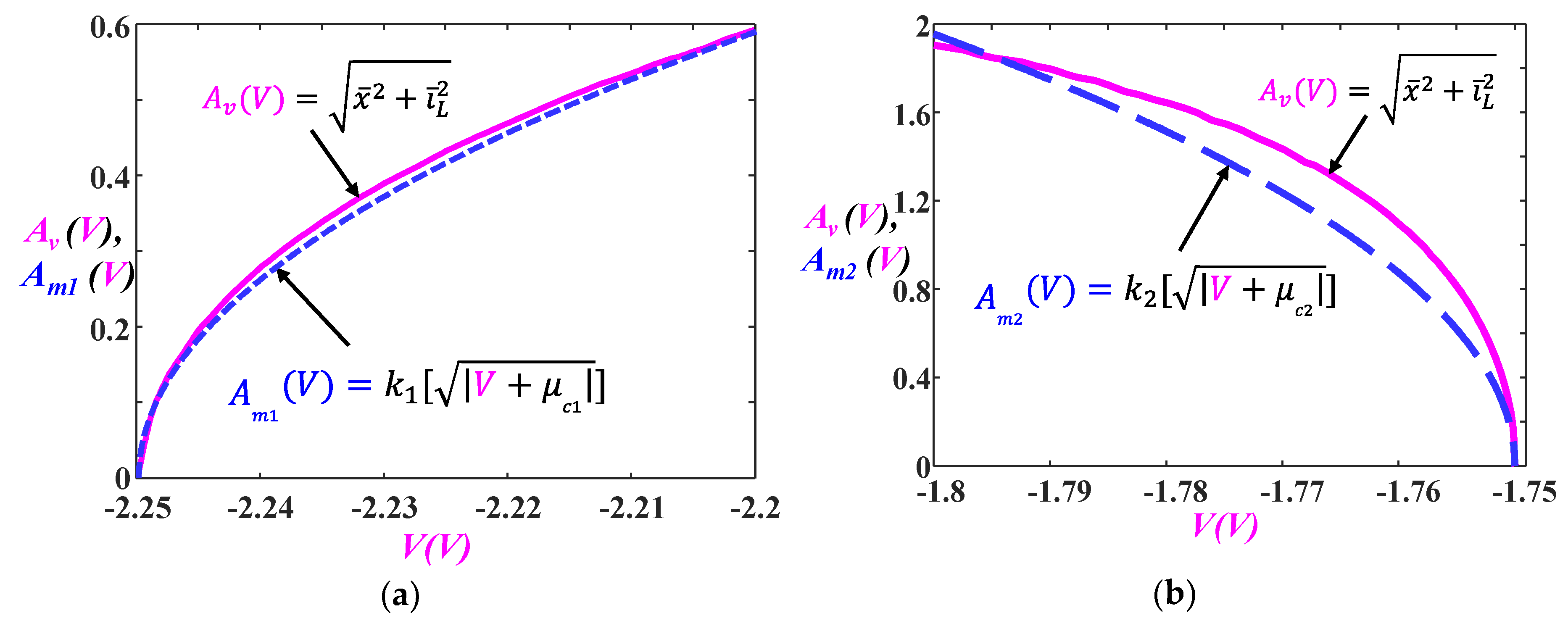
Hopf bifurcation points, shown in
Figure 6a,b, is quite similar to the curve computed from the analytical formulas (To avoid the emergence of complex number, the absolute value of (
µ − µc) is used in the analytical formulas. The critical parameters are
μc1 = −2.25
V and
μc2 = −1.75
V for 6-lobe
CCM and constants
k1 = 2.65 and
k2 = 8.75 are determined empirically for 6-lobe
CCM oscillator circuit [
16].)
and
with control parameter
µ = V and critical parameter
μc1 and
μc2 [
16]. In this review article, the supercritical Hopf bifurcation theorem is analyzed using 6-lobe
CCM oscillator circuit. However, the same bifurcation analogies and amplitude equations hold for 2-lobe and 4-lobe
CCM oscillator circuits except for the critical parameter of
μc1 and
μc2, and constants
k1 and
k2.
According to the supercritical Hopf bifurcation theorem [
26,
27], the 6-lobe
CCM oscillator circuit must exhibit a small stable near-sinusoidal oscillation, i.e., a
limit cycle, over a small range of
V beyond the critical parameter value (For better understanding about the choice of critical parameters
μc1 = −2.25
V and
μc2 =
−1.75
V please refer to Sect. 4.3 and Figure 13 of ref. [
16])
μc1 = V = −2.25
V.
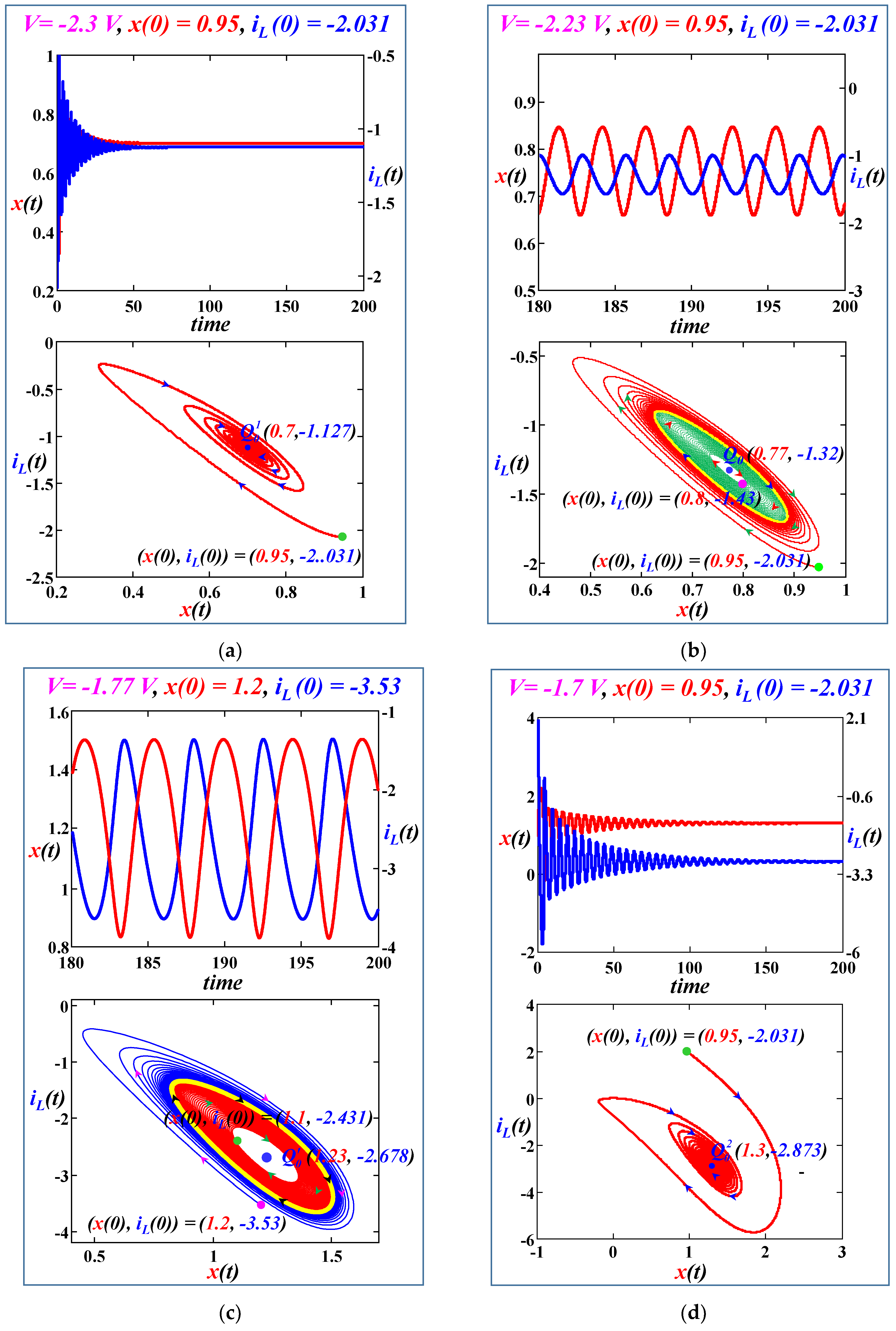
Figure 7a and d show that the transient waveforms converge to 2 asymptotically stable equilibrium points
for the parameter value
V = −2.3
V, (which is near, but to the left of the first Hopf bifurcation point
μc1 = V = −2.25
V (see inset of Figure 13 in ref. [
16])), and
for
V = −1.7
V (which is near, but to the left of the second Hopf bifurcation point
μc2 = V = −1.75
V), respectively. However, the transient waveforms generated by 6-lobe
CCM from two different initial states (
x(0) = 0.95,
iL (0) = −2.031) and (
x(0) = 0.8,
iL (0)
= −1.43) in
Figure 7b converge to the yellow stable limit cycle for
V = −2.23
V (which is near, but to the right of the first Hopf bifurcation point
μc1 = V = −2.25
V). Moreover, transient waveforms generated from two different initial states (
x(0) = 1.1,
iL (0) = −2.431) and (
x(0) = 1.2,
iL (0) = −3.53) for
V = −1.77 (which is near, but to the right of the second Hopf bifurcation point
μc2 = V = −1.75
V (see inset of Figure 13 in ref. [
16])) converge to a larger yellow limit cycle shown in
Figure 7c. The numerical simulation results shown in
Figure 7 affirm that the 6-lobe
CCM oscillator circuit exhibits a stable limit cycle when the bifurcation parameter
μ = V is chosen between the Hopf bifurcation points at
μc1 =
V = −2.25
V and
μc1 =
V = −1.75
V, as predicted by the supercritical Hopf bifurcation theorem [
16]. Similar supercritical Hopf bifurcation analogies also exhibits in 2-lobe and 4-lobe
CCM oscillator circuits [
13,
14,
15].
5. Physical Realization of CCM Family
Chua corsage memristors, shown in
Figure 8a, can be physically realized in circuit by including the switching kinetics closer to the behavioral attributes of each segment of PWL dynamic route map. A passive nonlinear-resistive two-port and a dynamic first-order one-port are cascaded to design an emulator circuit for
CCM memristor [
10], as shown in
Figure 8b. The passive nonlinear-resistive two-port is composed of parallel connected Graetz bridges [
17] with anti-serial diodes and the dynamic first-order one-port is made up of a
C-
R parallel circuit. Two set of Graetz bridge are used to supply double amount of input current to the dynamic first-order one-port, i.e.,
C-
R parallel circuit, for faster switching of memory states.
The DC
V-I curve of active and locally active resistor
R0 in dynamic one-port, in
Figure 8b, should exhibit the same number of contiguous breakpoints to that of the DC
V-I curves of
CCMs. For example, the DC
V-I curve of
R0 for 2-lobe
CCM emulator must have
two breakpoints, whereas, for 4-lobe and 6-lobe emulator the DC
V-I curve of
R0 should exhibit
four and
six contiguous breakpoints, respectively.
To design the nonlinear resistor
R0 for
CCM emulators, circuit theoretic analysis is conducted on opamps to obtain the desired DC
V-I breakpoints at specific voltages to that of
CC memristors. The driving point characteristic of a single positive and negative feedback op-amp circuit provides
two breakpoints on its piecewise linear DC
V-I curve [
28]. Therefore, only a single positive and negative feedback op-amp circuit is sufficient to design an active and locally active
R0 for 2-lobe
CCM emulator, as shown in
Figure 9a. However, two and three parallel-connected opamp circuits are required to design a
four and
six breakpoint piecewise linear DC
V-I curves for 4-lobe and 6-lobe
CCMs, respectively, as shown in
Figure 9b,c. The circuit theoretic analysis for designing the
CCM emulator circuit is conducted on 6-lobe
CC memristor, as it has the highest number of breakpoints on its contiguous
six lobes corsage DC V-I curve.
The circuit components and parameters of the parallel-connected opamps, in
Figure 9c, are exactly same except the negative feedback resistances (
R641,
R642, and
R643). The effective saturation voltage (
βEsat) of an individual op-amp circuit is determine by the negative feedback resistance which plays a crucial role to achieve the desired
V-I breakpoints at specified voltages, such as
V= ±3
V,
V= ±5
V, and
V= ±7
V (The 6-lobe
CCM has six breakpoints on its DC
V-I curve at
V = {
±3
V, ±5
V, ±7
V} as shown in
Figure 2c). However, the positive feedback path of the op-amp circuits might arise difficulties with the driving-point and transfer function. Such complication can be resolved by replacing the op-amp circuit with three ideal models, such as “
– Saturation region”, “
Linear region”, and “
+ Saturation region”. According to the circuit theoretic approach presented in [
12], the three ideal models generate the following combine current (
in) of an individual opamp circuit for an input voltage
v,
where n = {1, 2, and 3} denotes the operating opamp circuit.
Figure 10a shows the mathematically computed
V-in plots of the individual currents of opamp circuits. Observe that each
V-I curves has two breakpoints at specific voltage at
V = ± 2.82
V,
V = ± 4.95
V, and
V = ± 6.99
V. The value of the breakpoints are a bit dissimilar to that of 6-lobe
CCM (
V = {±3
V, ±5
V, ±7
V}) as the measured resistive parameters (
R631 =
R632 =
R633 = 0.985
K,
R661 =
R662 =
R663 = 100.5
K,
R671 =
R672 =
R673 = 1.001
K,
R641 = 3.888
K,
R642 = 1.797
K,
R643 = 0.987
K) are used in simulation.
The total current of parallel-connected opamp circuit is equal to the summation of all individual opamp currents,
The mathematical simulation of
V-I curve and the resistance of active and locally active
R0 (
R0 = V/I) are shown in
Figure 10b, whereas, the SPICE simulation and circuit implementation waveforms are shown in
Figure 10c, and d, respectively. Observe from circuit implementation waveforms, in
Figure 10d, that the locally active
R0 remains almost constant at R
01 = 137Ω over an input voltage range
−2.16
V < V < 2.16
V, except for a tiny interval at the origin. For ±2.16
V < V < ± 4.05
V, ±4.05
V < V < ±5.74
V, and
V > ±5.74
V, R0 increase from 137
Ω to 204
Ω, 204
Ω to 312
Ω, and 312
Ω to Rmax (very large resistance value), respectively. However, the increment rate of
R0 is dissimilar for each voltage range which reveals that the slope is constant in a particular voltage range, but inconstant for different voltage ranges. This suggests that the active and locally active
R0 exhibits four distinct memory states, namely,
R01,
R02,
R03, and
R04 as shown in
Figure 10b–d.
The numerical values of DC
V-I breakpoints and the resistance ranges of nonlinear resistor
R0 (in
Figure 10b–d) for mathematical modeling,
SPICE simulation, and circuit implementation are unequal. The reason behind such inequality is the non-ideal circuit components of the
SPICE module and the non-ideal characteristic of the implemented opamps along with noise induction from DC power supply and oscilloscope probe. Although the breakpoints of DC
V-I curves in
Figure 2c and
Figure 10b–d are quantitatively different, but qualitatively same. This reveals that the DC
V-I curve of any real nonlinear resistor can be converted into a memristor by applying the basic method explained in [
10,
11,
12] and [
18].
However, unlike a passive nonlinear-resistive two-port emulator circuit, the bi-stability and multi-stability phenomena of Chua Corsage Memristors can be realized by a single device as demonstrated in recent literature [
29,
30,
31]. The NbO
2 Mott memristor [
29,
30] exhibits an analogous dynamic route to that of 2-lobe
CCM which has two stable and one unstable equilibrium points on its dynamic route map (dT/dt vs. T (Figure 1 [
29])). The state switching attributes of NbO
2 memristor are identical to 2-lobe
CCM and regarded as bi-stable device. The universal formulas of switching kinetics (in
Section 3) can be applicable to NbO
2 Mott memristor as the PWL dynamic route, and switching kinetics are explicitly similar to 2-lobe
CCM. In addition, HfOx/AlOy-based homeothermic memristor [
31] has a similar number of stable equilibrium states (i.e., four temperature-dependent equilibrium states corresponding to its four dynamic conductances (Figure 3 in [
31])) to that of 6-lobe
CCM. When driven by DC input, the homeothermic memristor exhibits four distinct DC
V-I curves corresponding to its four temperature-dependent dynamic conductances (Figure 3e and f in [
31]) which is identical to 6-lobe
CCM (shown in
Figure 2c and
Figure 10). In spite of the quantitative dissimilarities, the NbO
2 Mott memristor and homeothermic memristor qualitative exhibit the bi-stability and multi-stability phenomena of CC memristors.
6. Concluding Remarks
This review article presents an in-depth and rigorous analysis of the nonlinear dynamical attributes, switching kinetics, and physical realization of Chua corsage memristors (CCMs). The versatile CCMs exhibit multiple stable equilibria on their complex and diversified, dynamic route map (DRM) and power-off plot (POP). Due to the presence of a higher degree of versatility in DRM, the CC memristors have a variety of dynamic paths in response to different initial conditions which reveals a highly nonlinear DC V-I curves. Unlike most published highly-nonlinear DC V-I curves which have several disconnected branches, the DC V-I curves of CCMs are contiguous. Moreover, the parametric representation and DC V-I curves of CCMs have an explicit analytical equation, which rarely happens.
The multiple stable equilibria on the DRM of CCMs reveal that it can be utilized as binary and multistate memory device whose exponential state trajectories for a particular linear piecewise segment, time period that required for the state trajectorial movement of the particular PWL segment, and the appropriate pulse amplitude and width that required for successful memory state switching can easily be determined from the universal formulas presented in Sect. 3. These universal formulas are applicable to any PWL DRM curves with any number of segments for any DC or pulse input.
Another impressive feature of CCMs is the locally active negative slope region of the DC V-I curves which gives rise to complex phenomenon, such as oscillation, by exploiting the edge of chaos and supercritical Hopf bifurcation theorem.
Last, but not least, the off-the-shelf active and locally active resistor (R0) in CCM emulators (designed with opamp or parallel-connected opamp circuits) is capable of emulating the attributes of the CCM DC V-I curves and proved that a memristor could be implemented using any real nonlinear resistor. Moreover, NbO2 Mott memristor and HfOx/AlOy-based homeothermic memristor reveals that the bi-stability and multi-stability phenomena of Chua corsage memristors can also be realized with a single physical device.
