Abstract
Gallium nitride (GaN) devices have been widely adopted to achieve high efficiency and high power density as alternative solutions to silicon devices. When the GaN power devices are used for variable frequency drive (VFD) systems, the high dv/dt pulses at the motor terminal, which induce shaft voltage and common mode current, should be carefully considered to ensure system reliability. Although the high dv/dt issues can be mitigated with a dv/dt filter method, it leads to performance degradation depending on cable length. Meanwhile, a matrix converter also becomes a next-generation power converter for the VFDs which has a regeneration capability and unity power factor. Thus, this paper discusses the GaN-based matrix converter for the VFD as a study case considering the motor terminal voltage quality and the common mode current. Also, a sine wave filter is adopted to cope with the terminal voltage quality irrespective of cable length. The optimized design procedure of the sine filter considers practical issues. Experimental results are presented to suggest a suitable solution for the GaN-based VFDs in accordance with the cable length.
1. Introduction
With the development of wide bandgap materials for power electronics such as gallium nitride (GaN), significant improvements in variable frequency drive (VFD) systems are expected. There are various advantages of GaN power devices, which are a much faster switching speed, higher breakdown voltage, higher thermal conductivity, and lower conduction resistance than the conventional silicon (Si) power devices [1,2]. Their strength can be a comprehensive solution to meet the high demand in industrial drive systems since GaN-based VFDs offer high efficiency, high power density, and high temperature operation.
While the GaN-based VFDs (using a standard three-phase two-level voltage source inverter) are commercially available in the industry, a matrix converter is becoming a popular alternative for next-generation motor drive systems [3,4,5,6,7]. Figure 1 shows the typical two-level voltage source inverter and the matrix converter block diagram for the VFDs. Compared to standard three-phase voltage source inverters using pulsewidth modulation (PWM) techniques, the matrix converter not only provides sinusoidal input current, but also operates with a unity input power factor. Moreover, it has a regeneration capability which cannot be achieved in the standard VFDs configuration. The most interesting point of the matrix converter topology is that it does not have a dc-link structure by using a bidirectional switch configuration which has reverse blocking and current conduction capability in both directions. The benefits of the matrix converter match well with the purpose of the GaN-based VFDs, especially for the high power density requirements.
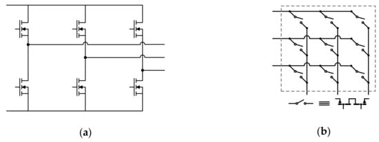
Figure 1.
Power converter circuit for variable frequency drive (VFD). (a) Conventional two-level inverter; (b) Matrix converter.
However, there is a significant problem to address before the GaN power devices are adopted in the motor drive system. The advantage of fast switching speed for the VFDs would negatively affect the motor reliability due to its high speed switching which results in high dv/dt at the motor terminal. It is important to appropriately apply the motor terminal voltage which causes motor insulation problems and bearing fluting damage. When the high dv/dt (by the inherent characteristics of GaN-based VFDs and the parasitic elements in the board layout) is applied at the motor terminal, unequal voltage distribution occurs at the first motor winding turn which leads to insulation failures between phase to phase or phase to motor frame [8,9,10]. Also, it generates an unwanted shaft voltage and bearing currents (which induce excessive motor heating, audible noise, vibration, and common mode current) through parasitic capacitance and inductance inside the motor. As a consequence, an efficient system operation cannot be achieved due to its maintenance cost as well as a decrease of lifetime [11,12,13,14,15,16,17,18,19,20,21].
A long cable between the VFDs and motor also has a non-negligible effect on the performance and reliability of the motor considering the practical installation environments such as deep sea and manufacturing plants. Voltage reflection, which is a well-known phenomenon, occurs where there is an impedance mismatch between the VFDs and the motor [18,19,20,21]. It would cause undesired voltage amplification (nearly twice the magnitude of the switching voltage) at the motor terminal and become worse as the cable length increases. A simple way to deal with this high dv/dt issue is to adjust the switching speed of the GaN devices by increasing the gate resistance. However, this approach has an inherent tradeoff between the terminal voltage quality and the switching loss of the GaN devices.
To address this issue, various output filter options have been studied in the literature. In [22,23,24,25,26,27], a dv/dt filter is proposed to mitigate the high dv/dt issues by using a damping resistor. Although it could provide the desired dv/dt slope (the rise time and fall time of the terminal voltage variations), the damping performance is vulnerable to the cable length, which cannot provide the designed dv/dt slope and settling time. On the other hand, a sine wave filter was studied to overcome the limitation of the dv/dt filter regardless of the cable length [25,26,27,28,29]. It is possible to apply a pure sinusoidal voltage to the motor terminal without the high dv/dt issues. Table 1 compares the characteristics of the dv/dt and sine wave filter. The sine wave filter option is mostly used for the high power machines and the high speed motor drives. For the high power machines where the stator winding inductance is small, the sine wave filter can effectively mitigate the motor’s current ripple. Also, it is usually adopted for the high speed motor drives where high switching frequency is needed for high speed control bandwidth. Meanwhile, with the emergence of the GaN power devices for the VFDs, it has become easier to use the sine wave filter in the GaN-based VFDs for the low power machines though it has some difficulties for the Si-based VFDs due to the size and cost of the filter, where the switching frequency cannot be increased to reduce the filter size. In other words, the GaN-based VFDs with the sine wave filter meet industrial and commercial demands for the high power density and high reliability of the motor drive systems.

Table 1.
Comparison of dv/dt filter and sine wave filter.
This paper contributes to the understanding of the output sine wave filter for the GaN-based VFD using the matrix converter topology as a study case. The main objective of this paper is to evaluate the comprehensive performance on the GaN-based VFD for the drive system considering the motor terminal voltage quality and common mode current with regard to sine filter and cable length. With this purpose, a suitable design consideration and a detailed performance analysis for the low power general purpose motor drives are discussed in this paper. In Section 2, the design of the sine wave filter and practical considerations are introduced to optimize the output filter considering the GaN-based VFDs. Section 3 presents experimental results of the GaN-based VFD in accordance with the output filter and cable length, and the performance analysis. Section 4 concludes and summarizes this paper.
2. Sine Wave Filter in GaN-Based VFD Applications
The sine wave filter with the GaN-based VFD configuration is shown in Figure 2, where the matrix converter is used for the VFD and the induction motor is connected to the VFD through the power cable. Various parasitic elements exist in the induction motor as illustrated in Figure 2. As mentioned earlier, if there is no proper way to mitigate the high dv/dt, it worsens the motor winding insulation and induces the common mode current icommon due to the parasitic capacitances. The International Electrotechnical Commission (IEC) standards were developed to manage the VFD systems of a sustainable environment [30]. Table 2 shows the IEC standards for motor terminal voltage quality according to the motor rated voltage Vrated. Thus, the use of the GaN devices in the VFDs should be carefully designed to meet the standards.
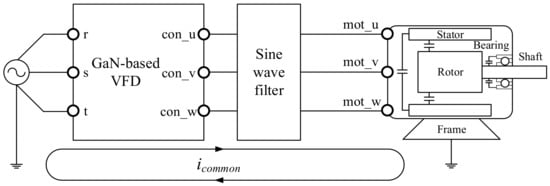
Figure 2.
System configuration of GaN-based VFD with sine wave filter.
Table 2.
IEC Standards for motor voltage quality.
2.1. Effect of High dv/dt on Motor Drive System
As mentioned in the previous section, the high dv/dt pulses worsen the motor system reliability through interactions with the motor parasitic elements which lead to the bearing and the common mode current [8,12,13,14,31]. Figure 3 shows a simplified equivalent circuit of the common mode current and the leakage current in the electric motor, where RS is the winding resistance, LS is the winding inductance, CSG is the stator to ground capacitance, CSR is the stator to rotor capacitance, CRG is the rotor to ground capacitance, and SB represents the dielectric breakdown between the inner and outer race. As shown in Figure 3a, the bearing voltage can be generated from the common mode voltage as the ratio of the parasitic capacitances. As the switching speed increases, the common mode current increases due to its low common mode impedance at the high frequency region [14].
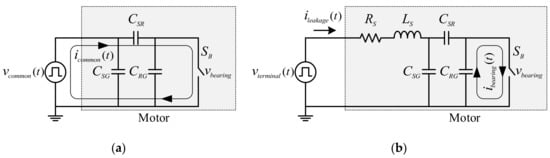
Figure 3.
Simplified equivalent circuit of (a) common mode and (b) leakage current.
Also, it is confirmed that the motor terminal voltage vterminal, which has a high dv/dt from the VFDs, induces the leakage current ileakage and the bearing current ibearing, as shown in Figure 3b. The leakage current can be expressed by using the motor parasitic elements in the time domain as follows.
Equation (1) indicates that the high dv/dt spikes at the motor significantly increase the magnitude of the leakage current, even without consideration of the bearing voltage and the cable impedance. In terms of the voltage reflection phenomenon which is caused by the impedance mismatch between the motor surge impedance and the power cable, small power motor drive systems are more likely to suffer from the high dv/dt. Since it has much larger surge impedance compared to a high power electric motor, the ratio of the impedance mismatch deteriorates further. Table 3 summarizes the typical surge impedance of the induction motor and the cable which is used in this paper [21].
Table 3.
Typical surge impedance of motor and cable.
2.2. Design of Sine Wave Filter
Figure 4 shows a per-phase equivalent circuit of a sine wave filter, where Lf is the filter inductance, Cf is the filter capacitance, and RL is the parasitic resistance of the filter inductor. From Figure 4, the transfer function of a sine wave filter can be derived as follows.
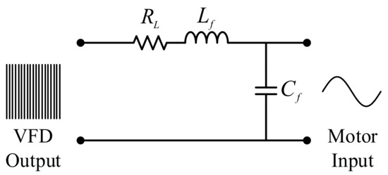
Figure 4.
Per-phase equivalent circuit of sine wave filter.
For the parameter selection of the sine filter, it is important to determine the resonant frequency of the sine wave filter, because the fundamental purpose of the filter is to achieve a pure sinusoidal voltage for the motor by rejecting the high frequency PWM voltage. The resonant frequency should be determined to avoid filter resonance between the fundamental frequency to the switching frequency. Meanwhile, the conventional Si-based VFDs make it difficult to select the resonant frequency for the sine filter due to its low switching frequency (e.g., 2 kHz to 8 kHz is usually used for the Si-based VFDs). In other words, it is not a suitable option for the industrial VFDs because of the large filter size and parameters.
Figure 5 shows the curves of the filter inductance and the filter capacitance in accordance with the resonant frequency, which is determined to avoid filter resonance as one-fourth of the switching frequency. In Figure 5, the higher filter inductance is preferred to reduce the filter capacitor current. However, the filter inductance should be limited by considering the voltage drop across the filter inductance at the rated output current. Although it can restrict the maximum value of the filter inductance, it cannot decide the minimum available value of the filter inductance and volume which can be the design parameters to achieve high power density. It is also not a proper approach for the small power motors, where the voltage drop is significantly low due to the low output current magnitude.
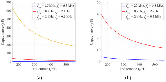
Figure 5.
Curves of (a) capacitance versus inductance for sine wave filter at 2 kHz, 8 kHz, and 25 kHz, (b) zoomed in view.
In order to achieve the optimum value of the sine wave filter, the filter inductance can be chosen considering the inductor volume and the switching frequency. In terms of the flux density, the physical volume of the inductor can be determined by the rated output current and the current ripple. Figure 6 shows the filter inductance and volume for the rated output current and the current ripple according to the switching frequency. The volume of the filter inductor is calculated by using the inductor design tool from Magnetics [32]. Here, the maximum ripple current is assumed not to exceed 4 A which is 40% of the peak current (10 A) at the rated condition in this paper. As the switching frequency increases from 10 kHz to 25 kHz, the inductor volume and the inductance are reduced to about 50% for the specified current ripple of 4 A. Although the required inductance is continuously reduced as the switching frequency increases, the volume of the inductor is nearly constant in the frequency range from 25 kHz to 40 kHz. Because of the flux density at the rated current, the volume of the inductor cannot be reduced further even with the higher switching frequency. Hence, by considering the inductor size and the system switching frequency, and the inductances for the sine filter can be selected as 25 kHz and 250 μH, which are used in this paper. Also, the filter capacitance can be chosen as 2.2 μF which offers the required filter resonant frequency as one-fourth of the switching frequency, 25 kHz.
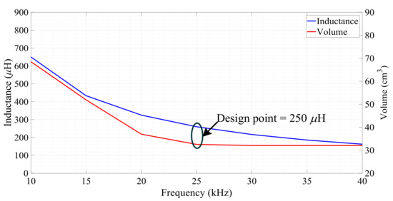
Figure 6.
Relation of inductance and volume according to switching frequency.
Figure 7 shows a frequency response of a designed sine wave filter (Lf = 250 μH, Cf = 2.2 μF), where fo is the fundamental output frequency, fr is the resonant frequency of the sine filter, and fsw is the switching frequency. It is confirmed that the cut-off frequency of the filter is 8.32 kHz, which is located between fo and fsw. Therefore, the high frequency PWM voltage of the VFDs is sufficiently mitigated by the sine wave filter without the resonance problem.
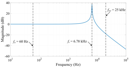
Figure 7.
Frequency response of sine filter.
3. Experimental Results
To validate the designed sine wave filter (Set 1. Lf = 250 μH, Cf = 2.2 μF) and GaN-based VFD in the motor drive system, the experiments were performed using a 1 kW induction motor and three phase 200 V input voltage source, as illustrated in Figure 8. Table 4 summarizes the system parameters of the GaN-based VFDs. For the bidirectional switches of the GaN matrix converter, the GaN power devices (Infineon, IGT60R070D) were used as shown in Figure 9a. One board is composed of three bidirectional GaN switches, and the matrix converter can be operated with the three board setup. Since the gate loop inductance and the power loop inductance influence gate-drive dynamics and voltage stress, the power and gate loop were carefully designed to minimize the loop inductance as much as possible. Based on the above design procedure, the prototype of the sine wave filter is employed as shown in Figure 9b.
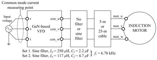
Figure 8.
Experimental setup.
Table 4.
System parameters.
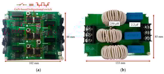
Figure 9.
Photograph of (a) GaN-based VFD using matrix converter and (b) sine wave filter.
Experiments were carried out to evaluate the motor terminal voltage quality and common mode current according to 5 m and a 25 m cable length. Also, two sets of comparative tests were conducted between the two sine filters with the same filter resonant frequency, as shown in Figure 8. The voltages and common mode current were measured with differential voltage probes (Lecroy, HVD3106A: 120 MHz bandwidth) and a current probe (Lecroy, CP150: 10 MHz bandwidth).
3.1. Motor Terminal Voltage
Figure 10 shows the measurement results of the line-to-line VFD output voltage vcon_uv, the line-to-line motor terminal voltage vmot_uv, and the motor phase current imot_u, where the sine wave filter was not adopted. In Figure 10a, where a cable length is about 5 meters, the rise time and the peak voltage of vcon_uv are 120 ns and 290 V. Although it has a sufficiently short cable length, the high frequency ringing and the voltage reflection phenomenon are observed in the motor terminal voltage vmot_uv due to the high dv/dt pulses of the GaN-based VFD (where the rise time and the peak voltage of vmot_uv are 60 ns and 365 V, respectively). For the 25-m cable length as in Figure 10b, the motor terminal voltage quality becomes even worse due to the voltage reflection phenomenon where the rise time and the peak voltage of vmot_uv are 70 ns and 492 V are seen. Considering the practical installation environments, the GaN-based VFDs may bring motor insulation breakdown (the dv/dt in 5-m cable: 6.1 kV/μs, and the dv/dt in 25-m cable: 7 kV/μs). Both Figure 10c,d, show the steady-state waveforms according to 5-m and 25-m cable length. As shown in the figure, the motor terminal voltage cannot be guaranteed by the motor standards.
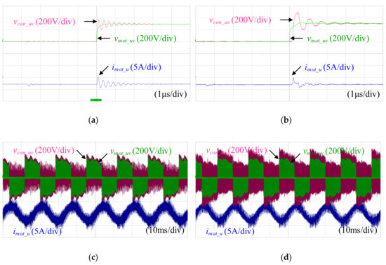
Figure 10.
Measurement results of GaN-based VFD without filter. (a,c) 5-m cable and (b,d) 25-m cable.
Figure 11 shows the experimental results of the GaN-based VFD with the two sets of the sine wave filters, where the line-to-line VFD output voltage is vcon_uv, the line-to-line motor terminal voltage is vmot_uv, and the motor phase current is imot_u. In both sine filters, the GaN-based VFD generates a pure sinusoidal voltage to the induction motor without the filter resonance. Compared to the no filter cases, the high frequency current ripple, which may induce the motor core and winding losses, cannot be observed in the motor current imot_u with the sine filter. Accordingly, as shown in the figure, it could deal with the IEC standards and improve the system reliability regardless of the cable length.
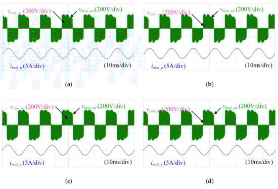
Figure 11.
Experimental results of GaN-based VFD with two sets of sine wave filter; (a) 5-m cable length, with sine filter (Lf = 250 μH, Cf = 2.2 μF); (b) 25-m cable length, with sine filter (Lf = 250 μH, Cf = 2.2 μF); (c) 5-m cable length, with sine filter (Lf = 117 μH, Cf = 4.7 μF); (d) 25-m cable length, with sine filter (Lf = 117 μH, Cf = 4.7 μF).
3.2. Common Mode Current
In order to experimentally evaluate the common mode current in the motor drive systems, a measurement configuration was established, as shown in Figure 8. As discussed before, it could be expected that the common mode current would decrease by using the sine wave filter. To further discuss, Figure 12 compares the frequency spectrum of the common mode current with and without the sine wave filters (Set 1. Lf = 250 μH, Cf = 2.2 μF, Set 2. Lf = 117 μH, Cf = 4.7 μF). In Figure 12a, where the cable length is 5 meters, the common mode current decreases especially in a high frequency range above 1 MHz. Compared to the 5-m cable cases, the common mode current increases in the frequency range below 1 MHz, especially in the switching frequency harmonics, as shown in Figure 12b, where the cable length is 25 meters. Here, it is interesting to note that the magnitude of icommon is reduced in the frequency range above 1 MHz which is related to the conducted electromagnetic interference emissions (150 kHz to 30 MHz). Meanwhile, both Figure 12c,d compare the frequency spectrum of icommon between the two sets of sine filters. By using the sine filter (Set 2. Lf = 117 μH, Cf = 4.7 μF), it also reduces the common mode current in high frequency regions above 1 MHz compared to the without filter case in both cable length conditions. However, compared to the sine filter of Set 1, it has a larger magnitude of the common mode current in the frequency range above 1 MHz due to the higher filter capacitance.
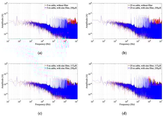
Figure 12.
Frequency spectrum comparison of common mode current with and without sine filter. (a,c) 5-m cable length and (b,d) 25-m cable length.
4. Conclusions
This paper investigates and discusses the comprehensive performance of the sine wave filter for the GaN-based VFDs using the matrix converter topology as a study case. The GaN-based VFDs offer various benefits of high efficiency and high power density. However, especially in the case of the GaN-based VFDs for the low power motor drive systems, the motor terminal voltage quality could become even worse due to a large impedance mismatch and the high dv/dt of the GaN devices. Thus, the sine wave filter is necessary to ensure the overall system reliability considering the practical installation environments where a long cable length is required for the deep sea and manufacturing plant. The design procedures are discussed to achieve optimal system parameters of the sine filter in the GaN-based VFD according to the switching frequency and filter volume. From the comparative performance evaluation of the terminal voltage and the common mode current, it is confirmed that the sine wave filter can be regarded as a suitable solution in GaN-based VFD applications for low power motor drives.
Author Contributions
Conceptualization, S.B. and Y.C.; Investigation, S.B. and D.C.; Project administration, Y.C.; Supervision, Y.C.; Validation, S.B. and H.B.; Writing—original draft, S.B. and D.C. All authors have read and agreed to the published version of the manuscript.
Funding
This work was supported by the National Research Foundation of Korea (NRF) grant funded by the Korean Government (MSIT). (No. 2017R1C1B2009425). This work was supported by “Human Resources Program in Energy Technology” of the Korean Institute of Energy Technology Evaluation and Planning (KETEP), granted financial resources from the Ministry of Trade, Industry & Energy, Republic of Korea (No. 20194030202370).
Conflicts of Interest
The authors declare no conflict of interest.
References
- Jones, E.A.; Wang, F.F.; Costinett, D. Review of commercial GaN power devices and GaN-based converter design challenges. IEEE J. Emerg. Sel. Top. Power Electron. 2016, 4, 707–719. [Google Scholar] [CrossRef]
- Chen, K.J.; Häberlen, O.; Lidow, A.; Tsai, C.l.; Ueda, T.; Uemoto, Y.; Wu, Y. GaN-on-Si power technology: Devices and applications. IEEE Trans. Elect. Devices 2017, 64, 779–795. [Google Scholar] [CrossRef]
- Kamruzzaman, M.; Barzegaran, M.R.; Mohammed, O.A. EMI reduction of PMSM drive through matrix converter controlled with wide-bandgap switches. IEEE Trans. Mag. 2017, 53, 1–4. [Google Scholar] [CrossRef]
- Metidji, B.; Taib, N.; Baghli, L.; Rekioua, T.; Bacha, S. Phase current reconstruction using a single current sensor of three-phase AC motors fed by SVM-controlled direct matrix converters. IEEE Trans. Ind. Electron. 2012, 60, 5497–5505. [Google Scholar] [CrossRef]
- Siami, M.; Khaburi, D.A.; Rivera, M.; Rodríguez, J. A computationally efficient lookup table based FCS-MPC for PMSM drives fed by matrix converters. IEEE Trans. Ind. Electron. 2017, 64, 7645–7654. [Google Scholar] [CrossRef]
- Xia, C.; Zhao, J.; Yan, Y.; Shi, T. A novel direct torque control of matrix converter-fed PMSM drives using duty cycle control for torque ripple reduction. IEEE Trans. Ind. Electron. 2014, 61, 2700–2713. [Google Scholar] [CrossRef]
- Siami, M.; Khaburi, D.A.; Rodríguez, J. Simplified finite control set-model predictive control for matrix converter-fed PMSM drives. IEEE Trans. Power Electron. 2017, 33, 2438–2446. [Google Scholar] [CrossRef]
- Erdman, J.M.; Kerkman, R.J.; Schlegel, D.W.; Skibinski, G.L. Effect of PWM inverters on AC motor bearing currents and shaft voltages. IEEE Trans. Ind. Appl. 1996, 32, 250–259. [Google Scholar] [CrossRef]
- Bonnett, A.H. A comparison between insulation systems available for PWM-inverter-fed motors. IEEE Trans. Ind. Appl. 1997, 33, 1331–1341. [Google Scholar] [CrossRef]
- Haq, S.U.; Jayaram, S.H.; Cherney, E.A. Insulation problems in medium-voltage stator coils under fast repetitive voltage pulses. IEEE Trans. Ind. Appl. 2008, 44, 1004–1012. [Google Scholar] [CrossRef]
- Martinez, W.; Odawara, S.; Fujisaki, K. Iron loss characteristics evaluation using a high-frequency GaN inverter excitation. IEEE Trans. Magn. 2017, 53, 1–7. [Google Scholar] [CrossRef]
- Chen, S.; Lipo, T.A.; Fitzgerald, D. Modeling of motor bearing currents in PWM inverter drives. IEEE Trans. Ind. Appl. 1996, 32, 1365–1370. [Google Scholar] [CrossRef]
- Chen, S.; Lipo, T.A.; Fitzgerald, D. Source of induction motor bearing currents caused by PWM inverters. IEEE Trans. Energy Conver. 1996, 11, 25–32. [Google Scholar] [CrossRef]
- Akagi, H.; Tamura, S. A passive EMI filter for eliminating both bearing current and ground leakage current from an inverter-driven motor. IEEE Trans. Power Electron. 2006, 21, 1459–1469. [Google Scholar] [CrossRef]
- Robles, E.; Fernandez, M.; Ibarra, E.; Andreu, J.; Kortabarria, I. Mitigation of common mode voltage issues in electric vehicle drive systems by means of an alternative AC-decoupling power converter topology. Energies 2019, 12, 3349. [Google Scholar] [CrossRef]
- Ren, X.; Liu, R.; Yang, E. Modelling of the bearing breakdown resistance in bearing currents problem of AC motors. Energies 2019, 12, 1121. [Google Scholar] [CrossRef]
- Concari, L.; Barater, D.; Toscani, A.; Concari, C.; Franceschini, G.; Buticchi, G.; Liserre, M.; Zhang, H. Assessment of efficiency and reliability of wide band-gap based H8 inverter in electric vehicle applications. Energies 2019, 12, 1922. [Google Scholar] [CrossRef]
- Han, D.; Li, S.; Wu, Y.; Choi, W.; Sarlioglu, B. Comparative analysis on conducted CM EMI emission of motor drives: WBG versus Si devices. IEEE Trans. Ind. Electron. 2017, 64, 8353–8363. [Google Scholar] [CrossRef]
- Akagi, H.; Hasegawa, H.; Doumoto, T. Design and performance of a passive EMI filter for use with a voltage-source PWM inverter having sinusoidal output voltage and zero common-mode voltage. IEEE Trans. Power Electron. 2004, 19, 1069–1076. [Google Scholar] [CrossRef]
- Skibinski, G.L.; Kerkman, R.J.; Schlegel, D. EMI emissions of modern PWM AC drives. IEEE Ind. Appl. Mag. 1999, 5, 47–80. [Google Scholar] [CrossRef]
- Saunders, L.A.; Skibinski, G.L.; Evon, S.T.; Kempkes, D.L. Riding the reflected wave-IGBT drive technology demands new motor and cable considerations. In Proceedings of the 1996 IAS Petroleum and Chemical Industry Technical Conference, Philadelpia, PA, USA, 23–25 September 1996; pp. 75–84. [Google Scholar]
- He, J.; Li, C.; Jassal, A.; Thiagarajan, N.; Zhang, Y.; Prabhakaran, S.; Feliz, C.; Graham, J.E.; Kang, X. Multi-domain design optimization of dv/dt filter for SiC-based three-phase inverters in high-frequency motor-drive applications. IEEE Trans. Ind. Appl. 2019, 55, 5214–5222. [Google Scholar] [CrossRef]
- Schroedermeier, A.; Ludois, D.C. Integration of inductors, capacitors, and damping into bus bars for silicon carbide inverter dv/dt filters. IEEE Trans. Ind. Appl. 2019, 55, 5045–5054. [Google Scholar] [CrossRef]
- Swamy, M.M.; Baumgardner, M.A. New normal mode dv/dt filter with a built-in resistor failure detection circuit. IEEE Trans. Ind. Appl. 2017, 53, 2149–2158. [Google Scholar] [CrossRef]
- Finlayson, P.T. Output filters for PWM drives with induction motors. IEEE Ind. Appl. Mag. 1998, 4, 46–52. [Google Scholar] [CrossRef]
- Swamy, M.M.; Kang, J.K.; Shirabe, K. Power loss, system efficiency, and leakage current comparison between Si IGBT VFD and SiC FET VFD with various filtering options. IEEE Trans. Ind. Appl. 2015, 51, 3858–3866. [Google Scholar] [CrossRef]
- Baek, S.; Cho, Y.; Cho, B.G.; Hong, C. Performance comparison between two-level and three-level SiC-based VFD applications with output filters. IEEE Trans. Ind. Appl. 2019, 55, 4770–4779. [Google Scholar] [CrossRef]
- Mishra, P.; Maheshwari, R. Design, analysis, and impacts of sinusoidal LC filter on pulsewidth modulated inverter fed-induction motor drive. IEEE Trans. Ind. Electron. 2020, 67, 2678–2688. [Google Scholar] [CrossRef]
- Lyu, Z.; Yang, M.; Xu, D.; Shang, S.; Xu, D. Design and research of GaN-based motor drive system with LC output filter. In Proceedings of the 10th International Conference on Power Electronics and ECCE Asia (ICPE ECCE Asia), Busan, Korea, 27–30 May 2019. [Google Scholar]
- International Electrotechnical Commission. IEC TS 60034-18-41 Rotating Electrical Machines-Qualification and Type Tests for Type I Electrical Insulation Systems Used in Rotating Electrical Machines Fed from Voltage Converters; IEC: Geneva, Switzerland, 2007. [Google Scholar]
- Liu, R.; Ma, X.; Ren, X.; Cao, J.; Niu, S. Comparative analysis of bearing current in wind turbine generators. Energies 2018, 11, 1305. [Google Scholar] [CrossRef]
- Magnetics Inductor Design. Available online: https://www.mag-inc.com/Design/Design-Tools/Inductor-Design (accessed on 5 January 2020).


© 2020 by the authors. Licensee MDPI, Basel, Switzerland. This article is an open access article distributed under the terms and conditions of the Creative Commons Attribution (CC BY) license (http://creativecommons.org/licenses/by/4.0/).