Article

Reconfigurable Power Converter for Constant Current Underwater Observatory

1
The Institute of Mechatronics Control Engineering, Zhejiang University, Hangzhou 310027, China
2
Ningbo Research Institute, Zhejiang University, Ningbo 315100, China
*
Author to whom correspondence should be addressed.
Electronics 2020, 9(2), 307; https://doi.org/10.3390/electronics9020307
Submission received: 14 January 2020 / Revised: 31 January 2020 / Accepted: 4 February 2020 / Published: 10 February 2020
(This article belongs to the Section Power Electronics)

Abstract

:
A constant current (CC) underwater observatory employing the shunt method to provide constant voltage (CV) power for external loads is favored in occasions where shunt-fault tolerance is required. However, low efficiency of CC to CV conversion with the shunt method limits its application, especially in scenarios of varying loads. In this paper, a highly reliable and stable CC/CV converter with better efficiency is introduced based on the proposed novel active soft bypass (ASB) technology and the proposed novel priority-based power management strategy (PPMS). The ASB technology is a method that employs switches and a special control sequence which greatly depresses the large voltage transient presenting on the input side when trying hard bypass redundant modules, and the PPMS makes the system easy to monitor and ensures the absolute reliability of ASB technology. The theoretical study of this novel reconfigurable CC/CV converter and validation experiments on a prototype are carried out, with results showing great improvement in the performance. In addition, the proposed reconfigurable power converter is applied to a coastal observatory in the East China Sea.

1. Introduction

Underwater observatories that enable long-term, real-time, in-situ observation of the oceans are widely applied in ocean exploration and research [1,2]. Power plays a key role in such kinds of underwater systems, where two main power solutions are employed including alternative current (AC) and direct current (DC). AC solution dominates the terrestrial power system, however, the DC distribution system, which is further classified into modes of constant current (CC) and constant voltage (CV) [3], is preferred if the cost of underwater deployment is considered [4]. Due to the merit feature of shunt fault tolerance, CC mode observatories are widely adopted at scenarios requiring uninterrupted observation even with fault presence [5]. Existing CC observatories systems, including the Hawaii Undersea Geo-Observatory (HUGO) [6], the Hawaii-2 Observatory (H2O) [7,8], ALOHA Cabled Observatory (ACO) [9], the Development of Dense Ocean-floor Network System for Earthquakes and Tsunamis (DONET) [10,11], DONET2 [12,13], the Marine Cable Hosted Observatory (MACHO) [14], the Japan Trench Earthquake and Tsunami Monitoring Network Project (S-net Project) [15,16,17], etc., are all powered by CC mode and mainly used for long term observation around unstable geology seismic areas.
Since most scientific instruments connected on nodes are powered by CV, CC to CV conversion is necessary. However, generally, underwater and terrestrial CC power systems are quite different. The underwater CC power system consists of multi-serial connection nodes that each tap a certain quantity of power from the constant current cable [18]. Considering stability problems due to parasitic parameters under long submarine cables, using a shunt regulator or similar principle to draw the required power is mainly used worldwide [19], such as HUGO, H2O, ACO, NONET, MACHO, DONET2 [6,7,8,9,10,11,12,13,14,15,16,17], etc. Figure 1a shows a typical CC/CV converter that comprises a shunt regulator and a DC/DC module [20]. The DC/DC module is an output unregulated converter and functions by stepping down voltage or boosting the current of the delivery power. The shunt regulator comprises a controller and a balance-load (BL, also known as the ‘dummy load’) [21]. By sampling the external load voltage, the controller adjusts the resistance of the BL to adapt the varying external load and keeps the total power unchanged by only balancing power consumed on the BL and external load. Then high stability is achieved as the input voltage remains unchanged by the constant input current. We can adopt a DC/DC module with high efficiency like the current to current series resonant converter (SRC) proposed in [22]. However, even so, a large amount of power still dissipates on the BL through heat when the external load is low [9], which induces a very low conversion efficiency compared to the terrestrial power system, as a compromise for the high stability of the system.
For underwater power systems, the extra cost of the wasted electricity is often very low compared with either the cost of manufacturing, deployment, or maintenance of the whole system. For CC underwater power systems with long cables, compared with sacrificing the stability of CC/CV conversion to put the whole system in danger, sacrificing efficiency to gain higher stability is often cost effective. Hence, for low power CC underwater systems, the single shunt method is often the first choice. Nonetheless, for high power CC underwater systems, a large amount of heat caused by low efficiency may affect the lifetime and reliability of the system. This also requires a more sophisticated heat dissipation design to fully reduce the ambient temperature. Therefore, it is still needed to improve the conversion efficiency as much as possible, while the stability of the system is not sacrificed.
One idea to improve efficiency is to adjust the system voltage when the load varies, which is known as the normal regulation method as shown in Figure 1b. Saha and co-workers [23] utilize the parallel resonant converter (PRC) to achieve the CC/CV conversion with a normal regulator, which is highly efficient. Based on the load-independent output voltage characteristics of the PRC in [14], Saha and colleagues [24] improve efficiency over a wide range of voltage and load power in a steady state. However, parasitic parameters under long submarine cables are not considered. Wang, Saha, and Zane [25] analyze the stability of an SRC with CC output being regulated in considering the cable effect, but only discuss the influence of small current fluctuation on the steady-state, whereas heavy load changes are not considered. Due to the presence of parasitic parameters such as the capacitance and inductance on long cables [25,26,27], the dynamic response of a long-cable CC system is relatively slow and the mentioned CC/CV methods may face challenges such as voltage oscillation or instability especially when heavy load change occurs [19]. The relatively low stability leads to relatively low reliability. Therefore, at present, considering stability and reliability issues, the CC/CV conversion with shunt regulation method is still the first choice rather than the normal regulation method in CC systems with long cables.
Another idea to improve efficiency is to adopt the stack structure consisting of multiple CC/CV modules, introduced by Kojima and colleagues [3] and Harris and Duennebier [19], in which redundant modules are bypassed to reach a better efficiency, as shown in Figure 1c. However, large voltage transient might be induced in such architectures during module bypassing due to the presence of long cables and the power supply, which may make the system vulnerable, namely, the reliability cannot be fully ensured. Take the converter with two stacked modules as an example (Figure 2a). In steady-state, the input voltages of two modules are theoretically the same and equal to half of the feeding source. When one module is simply bypassed (i.e., K is closed), due to the presence of parasitic capacitance of the long cable [28], assuming C >> C0 or C1, energy stored in C quickly charges the un-bypassed module and induces large voltage transient on its input side (i.e., voltage of C0 as shown in Figure 2b), that may cause permanent damage to the system. Although the actual situation is often much more complicated than this simple model. One goal of this paper is to solve this problem by studying a soft bypass technology under special strategy which can depress voltage transient while bypassing redundant modules as shown in Figure 2c. It is worth mentioning that various bypass methods are widely studied in the photovoltaic field [29,30,31]. However, in the photovoltaic field, each module has the characteristics of low voltage and small current. The bypass method cannot be directly applied to the CC underwater power system.
Aimed at solving the incompatibility of high stability, good reliability, and relatively high efficiency of the previous CC/CV converter used in a CC underwater observatory system, the active soft bypass (ASB) technology and the priority-based power management strategy (PPMS) are proposed in this work to improve the existing multi-module-stack structure. The relationship of these technologies is shown in Figure 3 and is explained in detail in the following sections. The proposed converter is specifically suitable for the CC underwater observatory system with relatively high power demand.

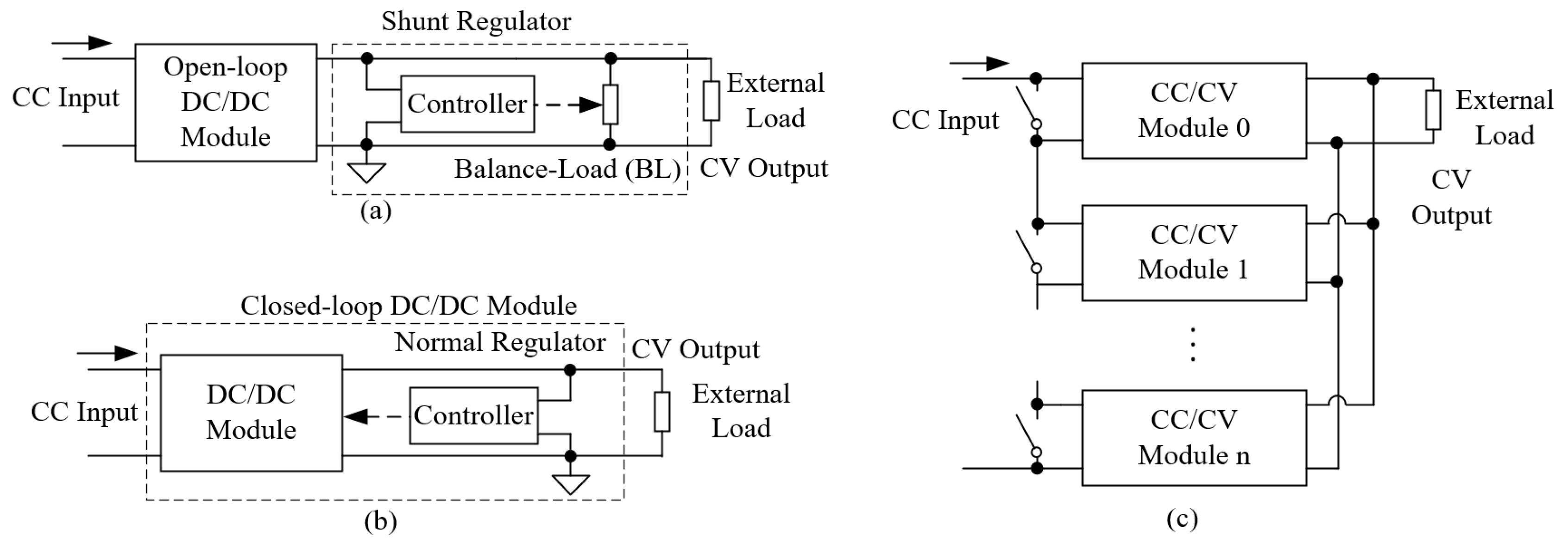
2. Reconfigurable CC/CV Converter

2.1. Overall Description

The proposed CC/CV converter with a multi-module-stack is shown in Figure 4. All modules, each having a topology as shown in Figure 1a and shunt-regulated individually, are stacked by series input and parallel output, through which a high-voltage input, medium-voltage output converter can be achieved [32,33]. When all modules are switched into running, the maximum output power is the sum of the maximum value of each module. In order to soft bypass the redundant module, module i (i = 1, 2, …, n, except the first module) is integrated with three additional switches KAi, KBi, and KCi, where KAi is parallel connected on the input side, and KBi and KCi bridge the output to the external load and current adjustable load (CAL), respectively. When KAi is closed, module i is bypassed and switched out of running. When KBi is closed, module i feeds power to an external load and when KCi is closed, module i feeds power to the CAL. KBi and KCi are interlocked so that the output can only feed power to one path. With these integrated switches and appropriate sequential control, the converter becomes reconfigurable. It is worth noting that minimum power is required to feed the local power such as switches control and communication, so the first module (module 0) should never be bypassed.

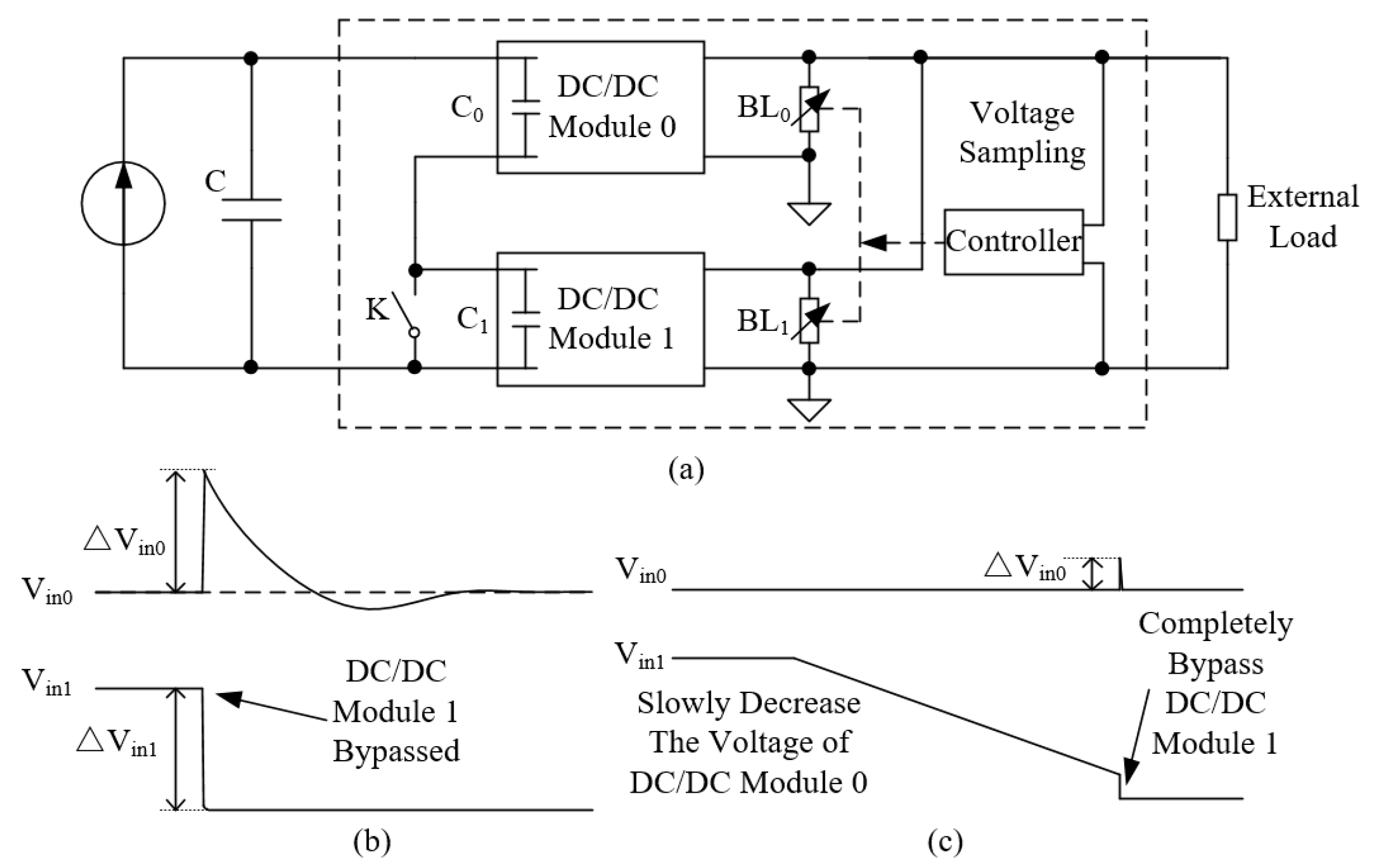
2.2. Active Soft Bypass and Reset Method

The main purpose of the ASB is to realize a smooth bypass of a CC/CV module. The design philosophy is to extend the time of the bypass procedure following a certain sequence. Firstly, the module i, which is supposed to be bypassed, is isolated from the external load bus by switching off KBi, meanwhile, hooked onto the CAL by switching on KCi. The CAL is a resistor and current controllable branch. Slowly reducing the equivalent resistance of CAL will gradually decrease the output voltage, in turn, the input voltages of module i. When the input voltage decreases to a very low value, KAi is switched on and KCi is switched off, then the module i is ultimately bypassed. With this control sequence, nearly zero voltage surge occurs on other modules while bypassing any module. During the period of regulating the resistance of the CAL, the inner BL of the module i performs the automatic balance-mechanism and regulation BL as well, which may prevent the soft bypass process. Therefore, the balance-mechanism of BL must be disabled and locked at the current state via the controller when the CAL is at work. The specific implementation method and sequence diagram are found in Section 3.
When module i needs to be switched on (or named reset), since no surge voltage is generated during reset, the reset process is much simpler: open KAi, enable the BL, and then close KBi when the module output voltage reaches a stable state.

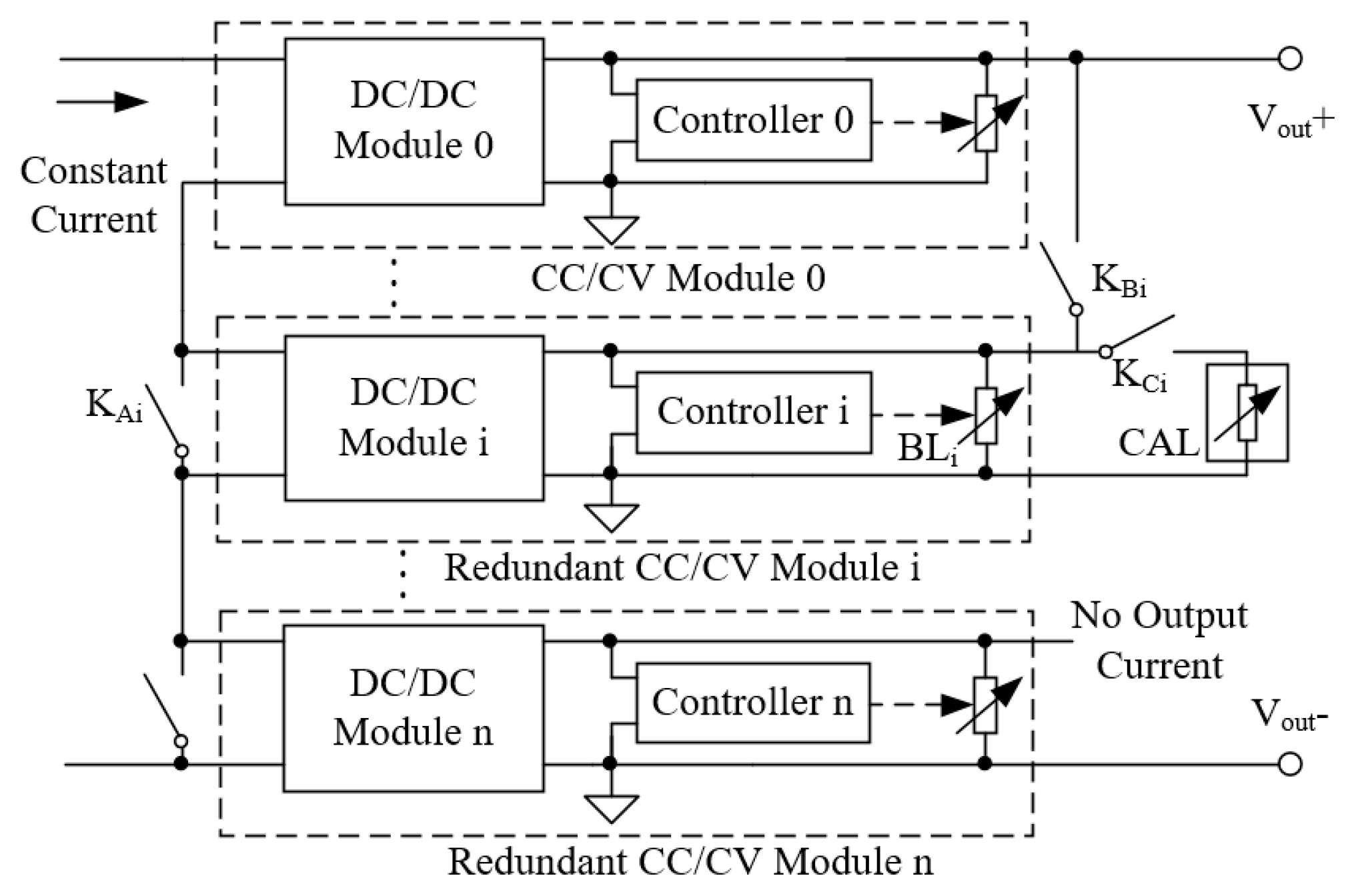
2.3. Priority-Based Power Management Strategy

To ensure better performance of the ASB, and also to provide a convenient power monitoring and management strategy, the PPMS is proposed and presented as follows.
In order to clarify the PPMS, the general power distribution of a multi-module-stack structure needs to be explained first. For a multi-module-stack CC/CV converter with the shunt regulators, there are n + 1 stacked modules, from module 0 to n. To attain an expected regulated voltage when powering a certain load, the sum of the delivery capability of each CC/CV module shall be equal to the power consumption of the BLs, the external load, and the switches, namely:
i = 0 n P m i = i = 0 n P B L i + P E x t e r n a l L + P K B + P K C .
The efficiency of the whole system can be obtained as:
η = P E x t e r n a l L i = 0 n P m i ξ i + P K B + P K C × 100 % ,
where Pm−i is the delivery capability of CC/CV module i, because of the existence of automatic balance-mechanism, it is equal to the output power of the DC/DC module in each working CC/CV module, namely, it is equal to the product of the output current of DC/DC and the output voltage set by the controller; PExternal−L is the power requirement of the external load; PBLi is the dissipating power on BLi; ξi is the efficiency of each DC/DC in CC/CV module i; PKB is the total dissipated power on switches KB which are in the closed states; PKC is the total dissipated power on switches KC which are in the closed states.
Although there are plenty of switches in the system, there is only one switch in close-state for each CC/CV module. When module i is reset, only KBi is closed while KAi and KCi are opened; when module i is bypassed, only KAi is closed while KBi and KCi are opened. KCi is closed only during the transitional process. If some switches with low close-state-resistance are selected, like solid state relay (SSR), the total power dissipated on the switches is quite lower compared with the total dissipated power of the BL. For ease of analysis, here we assume that all switches are ideal, namely, PKB and PKC are equal to 0.
From Equation (2), the most direct way to increase efficiency is to trim the total power close to PExternal−L, however, the total power is only configured by bypassing modules. Through the bypassing method, the efficiency may increase to some extent and depends on the actual external load and management strategy. Therefore, the management strategy is essential to reach high efficiency and stability.
The main idea of the PPMS is that each module consumes a constant amount of power with a part consumed by the external load and the rest by the corresponding BL, and each has a different priority to join-in the conversion; the higher priority means a higher chance to contribute power to an external load. While multiple modules are working at the same time, they will offer power to the external load one by one based on priority until meeting the external load requirement; therefore, if the external load requirement is obviously less than the total power of all running modules, the low priority module may contribute little power to the external load though it is working; and if it is more than the total power of all running modules, more modules will switch into conversion. Module 0 has the highest priority and is never switched off, and priorities of other modules gradually decrease following its index number. The smaller the index number of a module, the higher priority level it has.
The PPMS can be described by the following mathematical formulas. Supposing all modules are switched into conversion and powering a relatively stable load (or varying on a small scale) that satisfies Equation (3):
j = 0 i P m j < P E x t e r a n a l L < j = 0 i + 1 P m j , j = 0 , 1 , 2 i .
Then, the power dissipating on each BL satisfies Equation (4) under the PPMS.
P B L j = { 0 j = 0 i + 1 P m j P E x t e r a n a l L P m j ( j i ) ( j = i + 1 ) ( j > i + 1 ) .
Modules with j no more than i provide the full power to the external load and no power dissipating on BLj. Module with j = i + 1 provides power to both the external load and BLj at the same time. The balance-proportion depends on the actual load. Modules with j more than i + 1 contribute little power to an external load and all power are consumed by their own BL, which are called the redundant modules. For example, assuming a converter has 8 modules (i = 7) and each has Pmi = 100 W, when the required load is 430 W, then module 0 to 3 provides full power (100 W) to the external load, module 4 provides power to the external load (30 W) and BL (70 W) simultaneously and is balanced automatically according to load varying. Module 5 to 7 are recognized as redundant modules and obviously can be bypassed to reduce useless consumption if considering achieving better efficiency. If the load required increases during operation, bypassed modules are reset to join in the conversion.

2.4. The Link between ASB and PPMS

The PPMS ensures better performance of the ASB and reliability of the system. Assume there is a multi-module converter without the PPMS, in which, redundant power is equally dissipated by all BLs as follows:
P B L 0 = P B L 1 = = P B L i = ( j = 0 i P m j P E x t e r a n a l L ) / ( i + 1 ) < P m j .
From Equation (5), no redundant module exists. Suppose if trying to bypass one module to improve efficiency, such as module i, KBi will be open under a non-zero current state as the module provides certain continual power to an external load, which is a potential risk for long-term operations. After opening KBi, the redundant power will rebalance between BL0 to BL(i−1):
{ P B L 0 = P B L 1 = = P B L ( i 1 ) = ( j = 0 i 1 P m j P E x t e r a n a l L ) / i P B L i = P m i .
Power on BL0 to BLi is quite different before and after opening KBi, therefore, a rebalance-mechanism and process will occur during a moment of opening KBi, during which, the oscillating phenomenon may raise in some scale and is harmful to soft switching.
For a multi-module converter with the PPMS, however, before and after opening KBi, the power of each BL satisfies Equation (4). No power rebalance process exists between BLs (e.g., assume a two-module-converter with each module has maximum output power 100 W and the external load is 80 W). Before opening KB1, BL0 and BL1 share the 120 W redundant power, with each bearing 60 W respectively if without the PPMS. After opening KB1, BL0 only bears 20 W, whereas BL1 has to consume 100 W, a rebalance process of power on BL0 and BL1 from 60 W and 60 W to 20 W and 100 W occurs, and the KB1 switching current and transient fluctuation presents. However, based on the PPMS, before and after opening KB1, the power of BL0 and BL1 remains the same (PBL0 = 20 W and PBL2 = 100 W). Hence, the KB1 switching current and transient fluctuation are non-existent, and a complete ASB is achieved, so that a multi-module-stack CC/CV converter employing the ASB and the PPMS can depress surge voltage induced by power rebalancing among these modules and ensure switching KB under zero current. Therefore, the PPMS is a premise of the ASB method and also a guarantee of the reliability.
Another benefit of the PPMS and the ASB is that it is much easier to judge whether a specific CC/CV module can be bypassed. In the scenario where external load power is unknown, by measuring the current through KB or power on BL we can judge whether the corresponding module is fully redundant. The PPMS can provide sufficient information to the control system for further control such as bypassing this module.

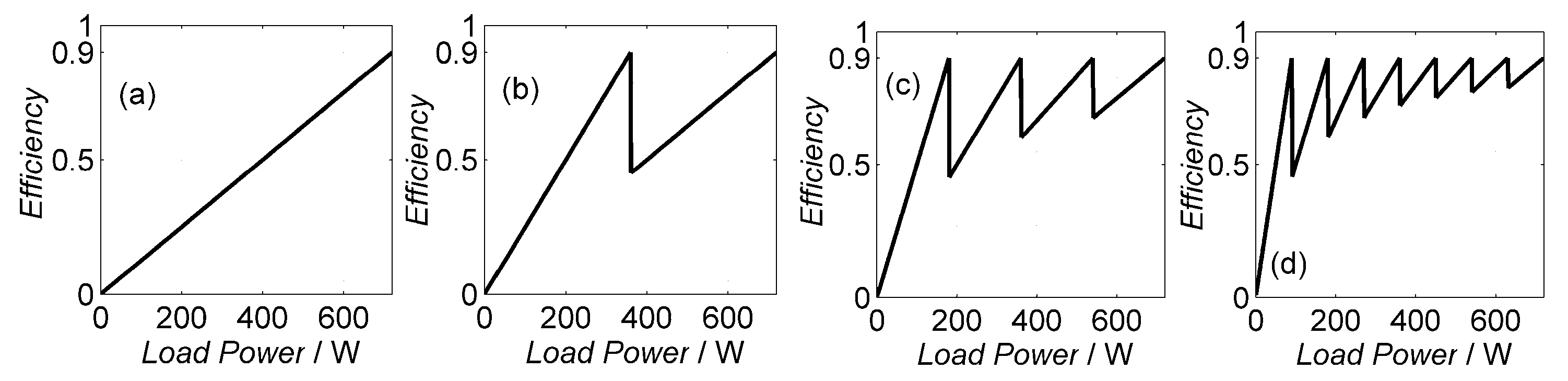
2.5. Efficiency Analysis

One object of reconfigurable power is reaching a more efficient conversion through bypassing redundant modules. Thus, the system only requires delivering power for external/internal loads and a very small part for the BL. Efficiency greatly improves comparing the approach of dissipating a large amount of power on the BL, and the more series connecting modules, the higher efficiency obtained. Through Equation (2), the efficiency comparison of different number modules of the reconfigurable converter is shown in Figure 5. The reconfiguration method improves the efficiency to a certain extent comparing to the no-power-reconfiguration case. However, meanwhile, simple reconfiguration also brings the stability issue. If the required external power fluctuates around the boundary where one module switches on/off, this module will be switched frequently if the load is slightly fluctuating and bringing unstable problems. Therefore, a hysteresis mechanism is necessary. Suppose modules 0 to i provide power to the load, and if the load is increasing when the external load plus an extra power Phys−U reaches the next module’s (here i + 1) reset conditions (Equations (7) and (8)), then module i + 1 is put into service. After module i + 1 is in service when the external load descends, the bypassing condition is not triggered until the external load plus an extra power Phys−L satisfies Equations (7) and (8). In order to realize a hysteresis condition, Phys−U must be smaller than Phys−L and the difference value ΔPhys= Phys−LPhys−U is a compromise of stability and efficiency; a large difference value induces better stability, however poorer efficiency and vice versa.
j = 0 i 1 P m j < P E x t e r a n a l L + P e x t r a < j = 0 i P m j , j = 0 , 1 , , n 1 ,
P e x t r a = { P h y s L P h y s U while   load   is   decreasing , while   load   is   increasing .
Therefore, how to decide and choose the setting of Phys−L and Phys−U is crucial if considering stability and efficiency. It depends on the actual feature of loads; however, it presents uncertainty. Considering practical application, 25%~40% of the delivery capability Pm−i for Phys−U and 5%~20% of Pm−i for hysteresis Phys−L are preferred as a suitable trade−off of stability and efficiency. For example, assume that a converter has 8 modules (i = 7), each has Pm−i = 90 W, and the efficiency ξ of DC/DC in each module is 0.9. If taking 40% allowance and 20% hysteresis, we can set Phys−L= 36 W and Phys−U =18 W. As shown in Figure 6, when the reconfiguration is performed, efficiency is relatively improved, which is opposite when reset is performed as a new module is put into service and most of power is dissipated only. Hysteretic loops are formed due to the different Pextra. If the external load fluctuates just around the switch−boundary (the points where the abrupt efficiency changes lie), due to the hysteresis feature, reconfiguration only presents once.

3. Implement of ASB and PPMS

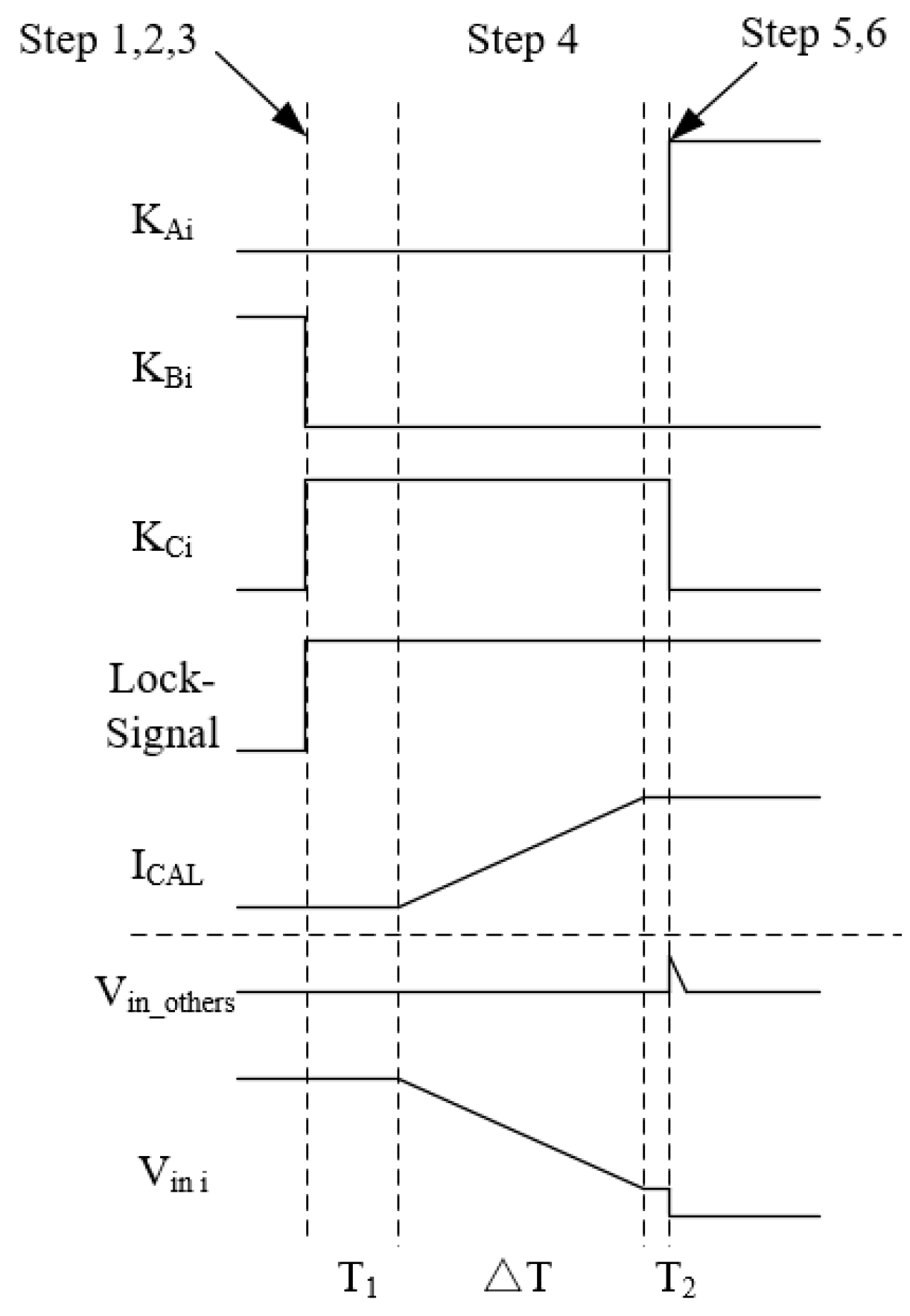
3.1. Time Sequence of ASB

Assuming module i is a redundant module and needs to be bypassed (Figure 7), the control sequence of ASB is described as follows. Supposing the initial state is: KAi is open, KBi is closed, KCi is open, and the lock-signal is invalid.
  • Open KBi to switch module i off from external load bus;
  • Disable the controller i by validating the lock-signal, so that BLi is locked at a fixed resistance;
  • Close KCi to switch module i onto the CAL;
  • Slowly reduce the resistance of the CAL, in turn, increase its current via control;
  • Close KAi to bypass the module i while its input voltage descends to a very low value;
  • Open KCi to isolate module i from the CAL.
Steps 1 to 3 are performed simultaneously, and steps 5 and 6 are performed simultaneously as shown in Figure 8.
The input current of the converter is constant, and the DC/DC module only functions by proportionally converting the input power, therefore, the output current is constant and proportional to the input current. Assume the output current is a constant I. When KBi is opened, and controller i is disabled to make BLi fixed at value Rlock (steps 1 and 2), it must satisfy the equation:
Rlock I = Vout,
where Vout is the output voltage before opening KBi and remains unchanged as its output impedance remains the same even after opening KBi. At the same time, the CAL is switched to the output side with infinite impedance (step 3), therefore, the CAL and BLi (resistance is fixed) share the power of this module. The following equation can be attained:
(Rlock//RCAL) × I = Vout = k Vin
where k is the transformation ratio of the DC/DC module, from which we know that the input voltage of this isolated module can be regulated by controlling the value of the RCAL. In order to soft bypass this module, the input voltage must be very low, so regulating RCAL from infinite gradually down to the minimum value is a reasonable solution (step 4). The minimum value depends on the hardware of the CAL, and the time of descending RCAL to the minimum value is ΔT. During this period, small turbulence may occur on other modules, however, it is negligible. When the input voltage descends to a relatively small value, such as only several volts, KAi can be closed in a much safer situation (step 5), and almost no ripper occurrs on other modules during this bypass process. It is also worth noting that T1 is designed to smooth fluctuations caused by the practical circuit when operating steps 1–3 and T2 is a delay of initial step 5. Both T1 and T2 are dependent on the practical circuit and preferred to obtain through tests.

3.2. The Realization of PPMS

The key of the PPMS is that each module has a different priority. Here we set each module with a different feedback reference value that is corresponding to priority level. A module with higher reference value will contribute the major power to an external load when multiple modules are parallelly connected. So, to achieve the PPMS, it is required that:
Vref0 > Vref1 > Vref2 > … > Vrefn,
PBLi−MAX = Pm−i, i = 1, 2, 3…n,
where Vrefi is the reference voltage of controller i, PBLi−MAX is the maximum power consumed by BLi at the reference voltage Vrefi, and Pmi is the constant output power of module i. The first requirement is achieved by designating controllers with different references (the difference between each other is very small). As for the second requirement, a BL consists of a power resistor and a series-connected and pulse width modulation (PWM) controlled metal-oxide-semiconductor field-effect transistor (MOSFET) as shown in Figure 9. We obtain:
RBLi = Ri_0/Di,
where RBLi is the equivalent resistance value of the BLi, Di is the duty ratio of the PWM, and Ri_0 is the resistance of the resistor in BLi. If Di varies between 0 and DiMAX, RBLi varies between Ri_0/DiMAX and infinite. When the controller regulates the output voltage to Vrefi, the consumption of BLi is as follows:
0 < PBLi = Vrefi2/(Ri_0/Di) < Vrefi2/(Ri_0/Di−MAX),
A higher priority level module has priority to contribute power first. The equivalent circuit of the DC/DC output side before opening KB is shown in Figure 9. Suppose module j is a higher level than module k and both are in services to power the same load. Due to the different references Vrefj > Vrefk, controller j tends to increase Vout whereas controller k tends to decrease it, so module j will increase the equivalent resistance of BLj, decrease the dissipating power on BLj and forward more power to the external load to boost up the Vout, and vice versa for module k. With the mutual contrast action of two modules, this process is actually a positive feedback rather than a nature-balance-mechanism, that behaves so the higher priority level module first provides power to the load. If module j has the ability to feed sufficient power to the load, Vout will be equal to Vrefj and reach a balanced state, spare power of module i will dissipate on its BLj, and all power of module k is spare and redundant. If module j fails to satisfy load requirements even if its power is all forward to load, then Vout will gradually decrease until equal to Vrefk, then module k starts to provide power to load and tries to obtain a balance state of Vrefk equal to Vout.
Take a two-module-stack converter as an example for easy comprehension. Supposing their voltage references are Vref0 > Vref1, module 0 has a higher priority than module 1. Other ratings are PBL0−MAX = Pm−0 and PBL1−MAX = Pm−1.
For the case of 0 < PExternal−L < Pm−0, both controllers will try to adjust the output voltage Vout equal to their own reference voltages. So, module 0 will increase the equivalent resistance of BL0, decreasing the dissipating power on BL0 and forward more power to the external load to boost up the Vout, in other words, module 0 first provides power to load. It has the capacity to satisfy external load, so Vout = Vref0. Spare power of module 0 will dissipate on BL0, and all power of module 1 is consumed on BL1 as follows:
{ P B L 0 = P m 0 P E x t e r n a l L P B L 1 = P B L 1 M A X = P m 1 .
For the case like PMAX0 < PExternal−L < Pm−0 + Pm−1, module 0 is unable to satisfy even all power forwarded to load. Module 1 would then provide further power to the load, leading to the output voltage regulated by controller 1 and reach a balanced state of Vout = Vref1. The power consumption is as follows:
{ P B L 0 = 0 P B L 1 = P m 0 + P m 1 P E x t e r n a l L .
Setting different references makes each module have different priorities to provide power to the external load, so that the converter realizes ASB and obtains higher efficiency; however, it brings the defect of low precise output due to multi-level voltage references, even though the differences are very small.

4. Simulations and Experiments

4.1. Prototype Parameters

A two-module-stack CC/CV converter prototype is constructed based on the structure shown in Figure 4 with n = 2. The main design parameters are shown in Table 1. Where Iin is the input current of the system; Iout0, Iout1 are the ratings of two output currents, respectively; ξi is the efficiency of the DC/DC module i; R0_0 and R0_1 are the resistor values in the BL0 and BL1 as shown in Figure 9, respectively; Vref0 and Vref1 are the reference voltages of controller 0 and controller 1, respectively. Therefore, Pm−0 = Iout0 × Vref0 = 88.8 W, Pm−1 = Iout1 × Vref1 = 87.9 W, PBL0−MAX = 92.2 W, PBL1−MAX = 90.3 W through Equation (14). Here, PBLi−MAX subjects to commercial-off-the-shelf resistors R0 in BL and is unable to fully satisfy Equation (12).

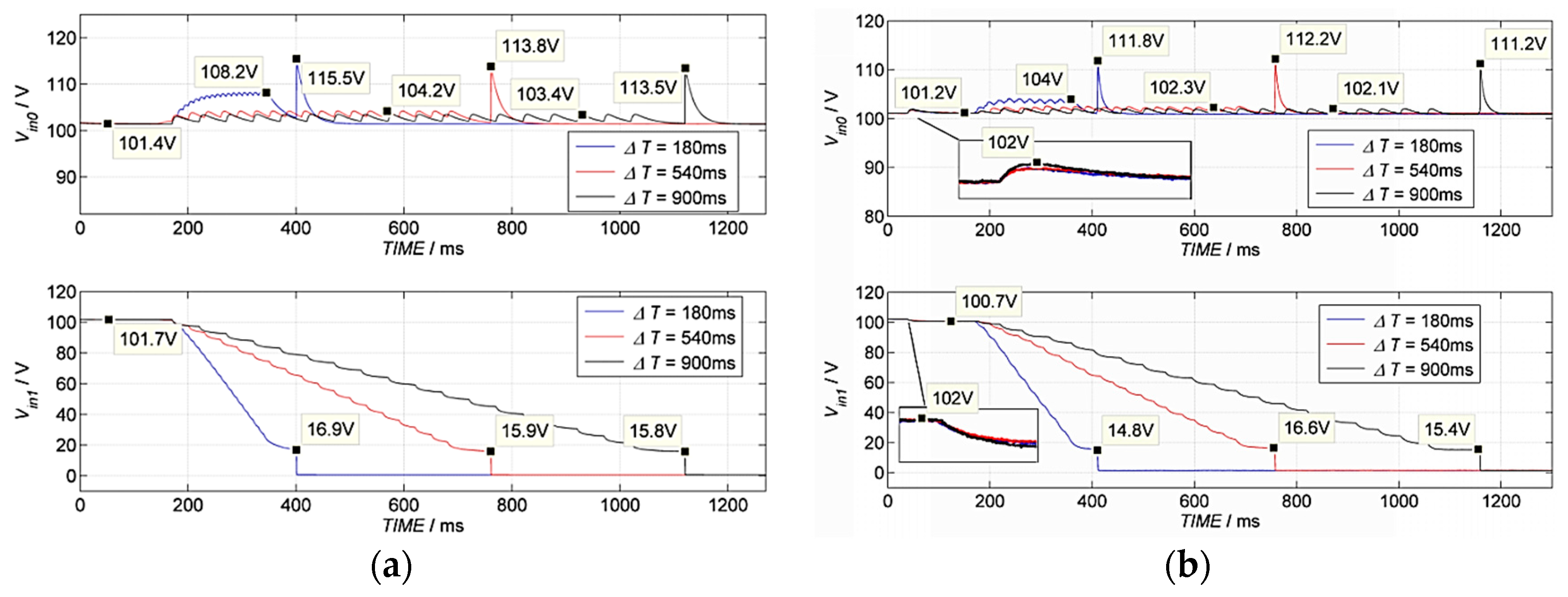
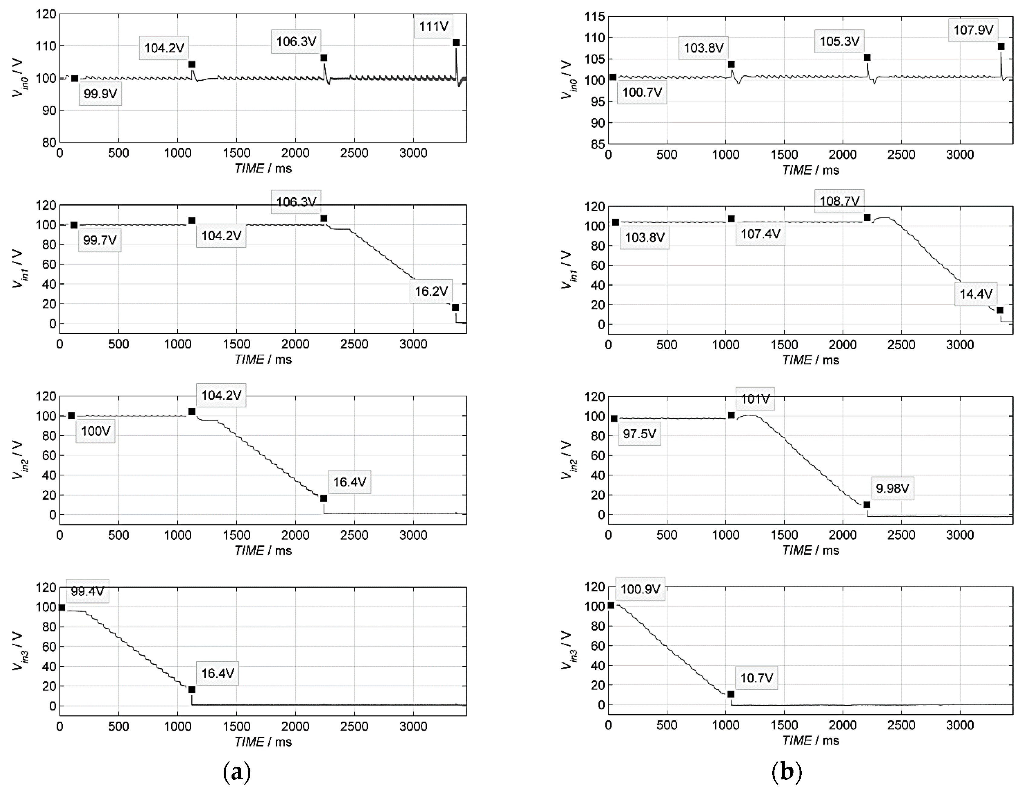
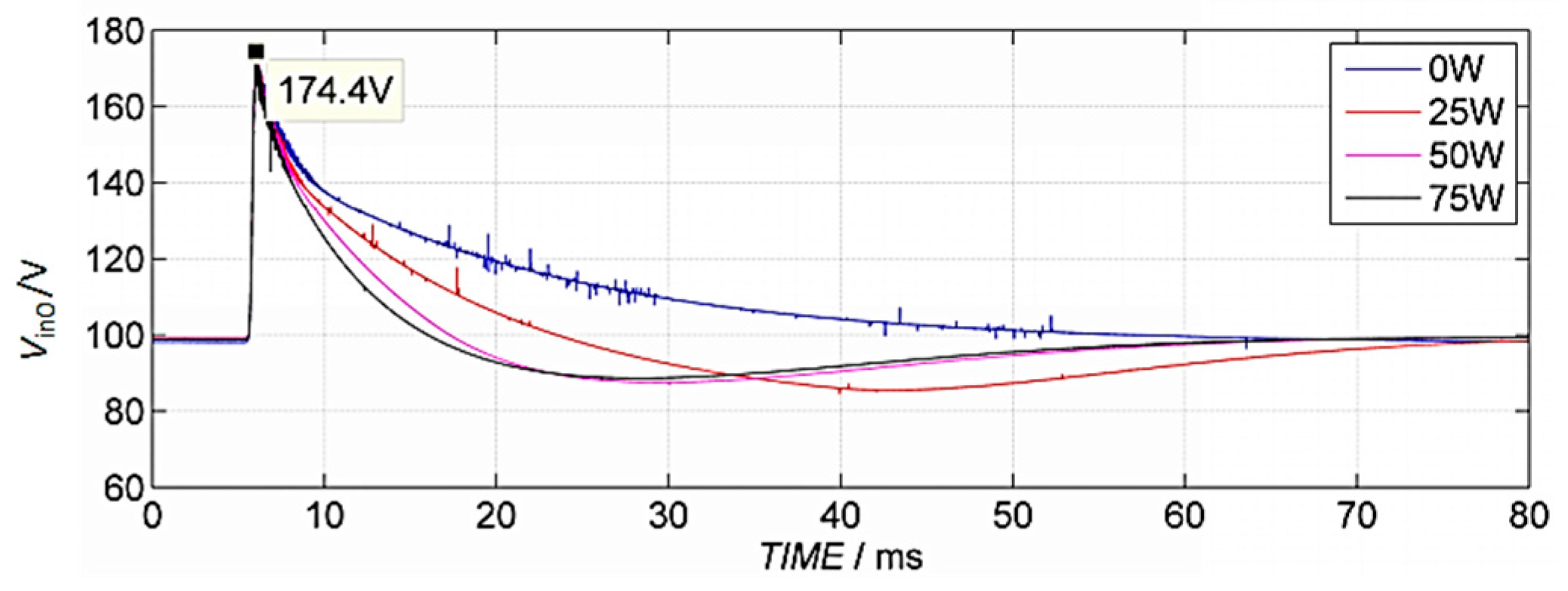
4.2. Simulated and Experimental Results of ASB

Aimed at soft bypassing modules in a serial connected CC/CV converter, the ASB and the PPMS improve both the reliability and the efficiency well. To validate the former object, we first implemented the simulation of hard bypass by closing switch KA directly on different loads when only module 0 and module 1 work normally, while the other two modules are bypassed. In this case, the feeding source was simplified with an ideal constant current source in parallel with a 147 μF capacitor to represent the non-ideal power supply. The simulating results of input of module 0 during hard bypass of module 1 are illustrated in Figure 10. The results show that a relatively large transient voltage occurred on the input side of module 0 when module 1 is directly bypassed without ASB, the overvoltage rose up to over 70% of rating. Different loads had little effect on this overvoltage, however, they mainly affected the time period of re-stabilization: the lighter the load, the longer the time.
In the same case, we applied the ASB and the PPMS both in the simulation and prototype. The value of ICAL was controlled by regulating RCAL discretely. Here ICAL was controlled varying from 0 A to 1.8 A in 18 steps with each increment being 0.1 A: T1 = 180 ms, T2 = 50 ms; ΔT = 180 ms, ΔT = 540 ms, ΔT = 900 ms. During the experiment, input voltages of two modules were observed. The results of simulation and experiments are illustrated in Figure 11. From the results, two periods were observed in each operation, the CAL regulating period and bypassing period. When the output was shifted to CAL which was gradually descending its resistance, the input voltage of module 1 (bypass target) descended synchronously in a nearly linear mode, however, the input voltage of module 0 rose slightly and rippled at a low overvoltage level. Different ΔT affected the raise latitude and ripple value. For example, for ΔT = 180 ms, the overvoltage was 8.2%, and the ripple was less than 1 V. When the module was bypassed, the input voltage of module 1 was tapped to zero directly, however, a small transient voltage occurred on module 0. The reason is that in a practical system, each module has to provide power to host load such as an individual controller so that a minimum output voltage is imperative. From the results, we could see around 16 V input voltage remained even at the moment of bypassing. Bypassing of this residual voltage caused a small surge of about 15 V on module 0 and then soon descended to zero in less than 50 ms. This residual voltage mainly depended on the host power; therefore, this surge voltage was little affected by different ΔT. From the figures, we also see that the experiment results are highly consistent with simulations.
In order to validate performances under different loads, simulation and experiment tests under loads of 0 W, 25 W, 50 W, and 75 W were carried out and results are shown in Figure 12a–d and Figure 13a–d, respectively. Due to the minimum residual voltage of bypassing period, different loads affected little on this surge voltage. Additionally, from the results, we conclude that the proposed ASB distinctly improved the performance under any loads compared with the case without ASB. The maximum surge voltages were 12.1 V, 11.4 V, 11.4 V, and 11.4 V respectively in simulations and 10.0 V, 10.2 V, 10.0 V, and 10.2 V respectively in experiments. Compared with the voltage spike shown in Figure 10 (174.4 V − 100 V = 74.4 V), our method reduces the spike by at least 83.7%.
In order to verify the performance of the ASB and the PPMS in a scenario where multiple modules are stacked, we bypass each module in the order “module 3 - module 2 - module 1”. The simulation and experimental results are shown in Figure 14a,b, respectively.

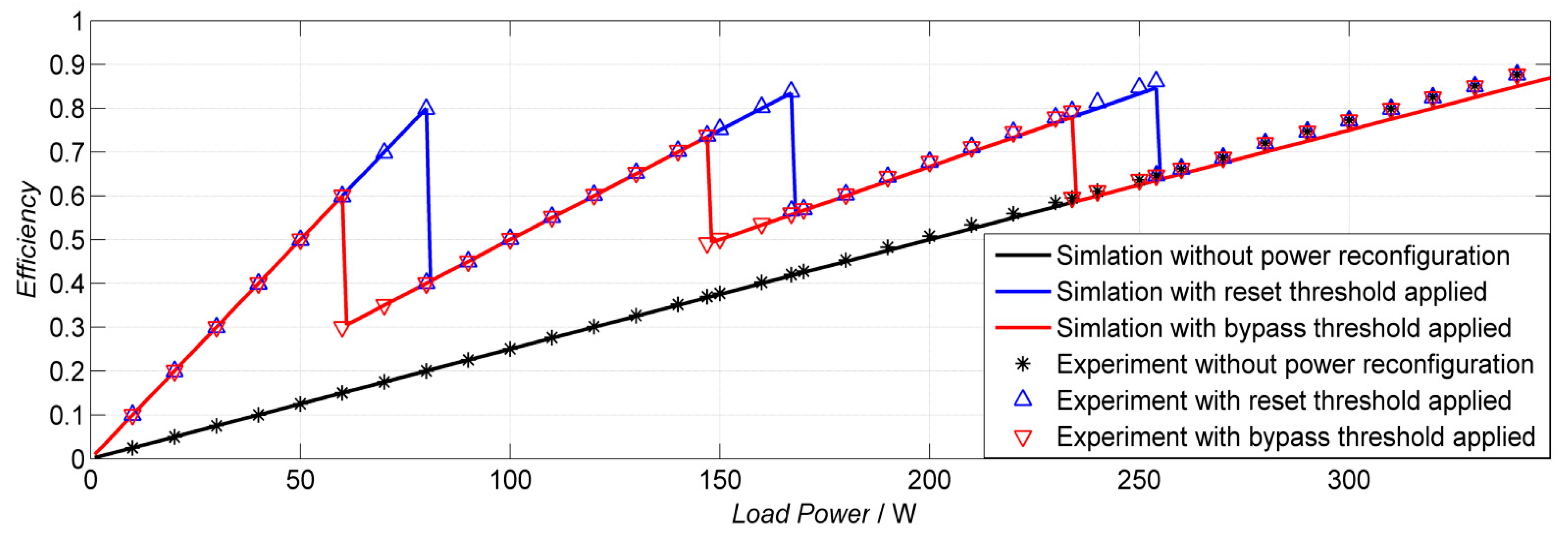
4.3. Efficiency Validation

In simulation and experiment, due to Phys−L = 27 W and Phys−U = 7 W, considering the rated output power of each module is about 87 W, the bypass thresholds are 60 W, 147 W, and 234 W, respectively; the reset thresholds are 80 W, 167 W, and 254 W, respectively. The simulation and experiment results of the efficiency in respect to the external load power are shown in Figure 15. In the experiment, when the load power is equal to each bypass threshold, reconfiguration was carried out, leading to the efficiency increasing from 0.300 to 0.600, 0.492 to 0.738, and 0.595 to 0.793, respectively. The load power is equal to each reset threshold. When the reset process was performed, efficiency reduced from 0.798 to 0.400, 0.838 to 0.560, and 0.862 to 0.647, respectively. The results of the simulation are highly consistent with the experimental results. Moreover, the hysteresis loop is clear in Figure 15. Furthermore, if the reconfiguration method was not applied, results are shown in Figure 15 as the black points and the black line. Efficiency was also remarkably improved with the reconfiguration applied. This action is also similar at other bypass/reset thresholds.

4.4. Sea Trial

A constant current observatory with a converter prototype based on the proposed methods was constructed as shown in Figure 16. This converter was stacked by two 100 W CC/CV modules that were powered with 1 A constant current, where module 1 could be softly bypassed based on the ASB and the PPMS (module 0 was configured with no bypass and reset method). It was used to power three scientific instruments including an underwater camera, a temperature, and depth sensors and a scientific sampling instrument. This observatory was successfully deployed off Zhairuo Island located at the mouth of Hangzhou Bay in South China Sea (122°4′21″ E, 29°56′22″ N). A 1 km long submarine cable was used to form a ring shape with this observatory located at around midpoint. During operation, three instruments could be controlled on-off remotely, and more importantly, when the external power was lower than 60 W or higher than 80 W, respectively, module 1 could be softly switched off or switched on, respectively. The reconfiguration can be controlled automatically or manually.

5. Conclusions

In this paper, a multi-module-stack CC/CV converter architecture with an ASB and PPMS is introduced. The system stability, reliability, and efficiency are well-considered:
  • The converter inherits the high stability of the shunt regulation method but overcomes the low-efficiency problem to a certain extent,
  • It overcomes the problem of low reliability of the typical multi-module-stack structure with the ASB and PPMS applied.
In addition, a prototype, where the methods in this paper were applied, was deployed on a constant current coastal ring shape observatory to power multiple underwater instruments. However, some other considerations need to be noted:
  • Compared with the typical multi-module-stack method, each module in the proposed architecture needs a corresponding closed switch, which may affect the efficiency to some extent.
  • Although the architecture is reliable because of the well-suppressed transient voltage, the converter will be very complex when there are a great number of stacked modules, which may in turn affect the reliability of the converter. Hence, the number of modules should not be too large.
  • Due to the adoption of the PPMS, the output voltage changes as a ladder-type-distribution with the load power. This also limits the number of stacked modules.

Author Contributions

Conceptualization and writing—original draft preparation, methodology, and formal analysis, Y.C. and Y.Z.; project administration and funding acquisition, Y.C. and C.Y.; validation and data curation, Z.D., H.Z., and G.M.; writing—review and editing, Y.C. and G.M. All authors have read and agreed to the published version of the manuscript.

Funding

This work was supported by National Natural Science Foundation of China (No. 51979246 and No. 41676089), and Natural Science Foundation of Zhejiang Province of China (No. LY18E090003).

Acknowledgments

The authors would like to thank Meiyan Pan for her valuable help with this paper.

Conflicts of Interest

The authors declare no conflicts of interest.

References

  1. Chave, A.D.; Waterworth, G.; Maffei, A.R.; Massion, G. Cabled Ocean Observatory Systems. Mar. Technol. Soc. J. 2004, 38, 30–43. [Google Scholar] [CrossRef]
  2. Chen, Y.; Yang, C.; Li, D.; Jin, B.; Chen, Y. Design and Application of a Junction Box for Cabled Ocean Observatories. Mar. Technol. Soc. J. 2012, 46, 50–63. [Google Scholar] [CrossRef]
  3. Kojima, J.; Howe, B.M.; Asakawa, K.; Kirkham, H. Power systems for ocean regional cabled observatories. In Proceedings of the Oceans ’04 MTS/IEEE Techno-Ocean ’04 (IEEE Cat. No.04CH37600), Kobe, Japan, 9–12 November 2005; Volume 4, pp. 2176–2181. [Google Scholar]
  4. Howe, B.M.; Kirkham, H.; Vorpérian, V. Power system considerations for undersea observatories. IEEE J. Ocean. Eng. 2002, 27, 267–274. [Google Scholar] [CrossRef]
  5. Asakawa, K.; Kojima, J.; Muramatsu, J.; Takada, T.; Kawaguchi, K.; Mikada, H. Current-to-current converter for scientific underwater cable networks. IEEE J. Ocean. Eng. 2007, 32, 584–592. [Google Scholar] [CrossRef]
  6. Duennebier, F.K.; Harris, D.W.; Jolly, J.; Caplan-Auerbach, J.; Jordan, R.; Copson, D.; Stiffel, K.; Babinec, J.; Bosel, J. HUGO: The Hawaii Undersea Geo-Observatory. IEEE J. Ocean. Eng. 2002, 27, 218–227. [Google Scholar] [CrossRef]
  7. Petitt, R.A.; Harris, D.W.; Wooding, B.; Bailey, J.; Jolly, J.; Hobart, E.; Chave, A.D.; Duennebier, F.; Butler, R.; Bowen, A.; et al. The Hawaii-2 Observatory. IEEE J. Ocean. Eng. 2002, 27, 245–253. [Google Scholar] [CrossRef]
  8. Butler, R. The Hawaii-2 Observatory: Observation of Nanoearthquakes. Seismol. Res. Lett. 2003, 74, 290–297. [Google Scholar] [CrossRef]
  9. Howe, B.M.; Lukas, R.; Duennebier, F.; Karl, D. ALOHA cabled observatory installation. In Proceedings of the OCEANS’11 MTS/IEEE KONA, Waikoloa, HI, USA, 19–22 September 2011; pp. 1–11. [Google Scholar]
  10. Kawaguchi, K.; Kaneda, Y.; Araki, E. The DONET: A real-time seafloor research infrastructure for the precise earthquake and tsunami monitoring. In Proceedings of the OCEANS 2008—MTS/IEEE Kobe Techno-Ocean, Kobe, Japan, 8–11 April 2008; pp. 1–4. [Google Scholar]
  11. Hishiki, K.; Fujiwara, N.; Katayama, T.; Mizukawa, T.; Kawaguchi, K.; Yokobiki, T. Power distribution system for multidisciplinary seafloor observatory junction box. In Proceedings of the 2016 Techno-Ocean (Techno-Ocean), Kobe, Japan, 6–8 October 2016; pp. 325–328. [Google Scholar]
  12. Choi, J.K.; Yokobiki, T.; Kawaguchi, K. ROV-Based Automated Cable-Laying System: Application to DONET2 Installation. IEEE J. Ocean. Eng. 2018, 43, 665–676. [Google Scholar] [CrossRef]
  13. Kawaguchi, K.; Araki, E.; Kogure, Y.; Takahashi, N.; Katayama, T.; Hishiki, K.; Fujiwara, N.; Iida, N.; Kaneda, Y. Development of DONET2-Off Kii chanel observatory network. In Proceedings of the 2013 IEEE International Underwater Technology Symposium (UT), Tokyo, Japan, 5–8 March 2013; pp. 1–5. [Google Scholar]
  14. Hsiao, N.-C.; Lin, T.-W.; Hsu, S.-K.; Kuo, K.-W.; Shin, T.-C.; Leu, P.-L. Improvement of earthquake locations with the Marine Cable Hosted Observatory (MACHO) offshore NE Taiwan. Mar. Geophys. Res. 2014, 35, 327–336. [Google Scholar] [CrossRef]
  15. Kanazawa, T.; Shinohara, M.; Sakai, S.; Utada, H.; Shiobara, H.; Yamada, T.; Mochizuki, K.; Yamazaki, K. New innovative ocean bottom cabled seismometer system and observation in the Sea of Japan. In Proceedings of the 2011 IEEE Symposium on Underwater Technology and Workshop on Scientific Use of Submarine Cables and Related Technologies, Tokyo, Japan, 5–8 April 2011; pp. 1–3. [Google Scholar]
  16. Shinohara, M.; Yamada, T.; Sakai, S.; Shiobara, H.; Kanazawa, T. New ocean bottom cabled seismic and tsunami observation system enhanced by ICT. In Proceedings of the 2014 Oceans—St. John’s, St. John’s, NL, Canada, 14–19 September 2014; pp. 1–6. [Google Scholar]
  17. Kanazawa, T. Japan Trench earthquake and tsunami monitoring network of cable-linked 150 ocean bottom observatories and its impact to earth disaster science. In Proceedings of the 2013 IEEE International Underwater Technology Symposium (UT), Tokyo, Japan, 5–8 March 2013; pp. 1–5. [Google Scholar]
  18. Barnes, C.R.; Best, M.M.R.; Johnson, F.R.; Pautet, L.; Pirenne, B. Challenges, Benefits, and Opportunities in Installing and Operating Cabled Ocean Observatories: Perspectives from NEPTUNE Canada. IEEE J. Ocean. Eng. 2013, 38, 144–157. [Google Scholar] [CrossRef]
  19. Harris, D.W.; Duennebier, F.K. Powering cabled ocean-bottom observatories. IEEE J. Ocean. Eng. 2002, 27, 202–211. [Google Scholar] [CrossRef]
  20. Chen, Y.; Xiao, S.; Li, D. Power system design for constant current subsea observatories. Front. Inf. Technol. Electron. Eng. 2019, 20, 1505–1515. [Google Scholar] [CrossRef]
  21. Takehira, K. Submarine system powering. In Undersea Fiber Communication Systems, 2nd ed.; Academic Press: Cambridge, MA, USA, 2016; pp. 381–402. ISBN 9780128042694. [Google Scholar]
  22. Wang, H.; Saha, T.; Riar, B.; Zane, R. Design Considerations for Current-Regulated Series-Resonant Converters with a Constant Input Current. IEEE Trans. Power Electron. 2019, 34, 141–150. [Google Scholar] [CrossRef]
  23. Saha, T.; Wang, H.; Riar, B.; Zane, R. Analysis and Design of a Parallel Resonant Converter for Constant Current Input to Constant Voltage Output DC-DC Converter Over Wide Load Range. In Proceedings of the 2018 International Power Electronics Conference (IPEC-Niigata 2018-ECCE Asia), Niigata, Japan, 20–24 May 2018; pp. 4074–4079. [Google Scholar]
  24. Saha, T.; Bagchi, A.C.; Wang, H.; Zane, R. Analysis and Design of Wide Range Output Voltage Regulated Power Supply for Underwater Constant Input Current DC Distribution System. In Proceedings of the 2018 IEEE 19th Workshop on Control and Modeling for Power Electronics (COMPEL), Padova, Italy, 25–28 June 2018; pp. 1–7. [Google Scholar]
  25. Wang, H.; Saha, T.; Zane, R. Impedance-based stability analysis and design considerations for DC current distribution with long transmission cable. In Proceedings of the 2017 IEEE 18th Workshop on Control and Modeling for Power Electronics (COMPEL), Stanford, CA, USA, 9–12 July 2017; pp. 1–8. [Google Scholar]
  26. Liukkonen, M.; Hinkkanen, M.; Kyyra, J.; Ovaska, S.J. Modeling of multiport DC busses in power-electronic systems. In Proceedings of the 2013 IEEE International Conference on Industrial Technology (ICIT), Cape Town, South Africa, 25–28 February 2013; pp. 740–745. [Google Scholar]
  27. Zhang, S.; Jiang, S.; Lu, X.; Ge, B.; Peng, F.Z. Resonance issues and damping techniques for grid-connected inverters with long transmission cable. IEEE Trans. Power Electron. 2014, 29, 110–120. [Google Scholar] [CrossRef]
  28. Chen, Y.H.; Zang, Y.J.; Yao, J.J.; Muhammad, G. Optimal communication frequency for switching cabled ocean networks with commands carried over the power line. Front. Inf. Technol. Electron. Eng. 2019, 20, 1331–1343. [Google Scholar] [CrossRef]
  29. Acciari, G.; Graci, D.; La Scala, A. Higher PV module efficiency by a novel CBS bypass. IEEE Trans. Power Electron. 2011, 26, 1333–1336. [Google Scholar] [CrossRef]
  30. Dalessandro, V.; Guerriero, P.; Daliento, S. A simple bipolar transistor-based bypass approach for photovoltaic modules. IEEE J. Photovolt. 2014, 4, 505–513. [Google Scholar] [CrossRef]
  31. Qian, W.; Peng, F.Z.; Han, S. The faulty module bypass for thermoelectric generation. In Proceedings of the 2010 Twenty-Fifth Annual IEEE Applied Power Electronics Conference and Exposition (APEC), Palm Springs, CA, USA, 21–25 Februaty 2010; pp. 2288–2293. [Google Scholar]
  32. Siri, K.; Willhoff, M.; Truong, C.; Conner, K.A. Uniform voltage distribution control for series-input parallel-output, connected converters. In Proceedings of the IEEE Aerospace Conference Proceedings, Big Sky, MT, USA, 4–11 March 2006; pp. 1–12. [Google Scholar]
  33. Chen, W.; Zhuang, K.; Ruan, X. A Input-Series- and Output-Parallel-Connected Inverter System for High-Input-Voltage Applications. IEEE Trans. Power Electron. 2009, 24, 2127–2137. [Google Scholar] [CrossRef]
Figure 1. The typical and classical CC/CV (constant current/constant voltage) power transformation architectures used in the CC observatories systems: (a) The single CC/CV module with the shunt regulator, which may cause large energy waste. (b) The CC/CV module with the normal regulator, which may face some stability problems due to the effect of the long cables. (c) The multi-module-stack structure based on the single CC/CV module with the shunt regulator, in which the large voltage transient might be induced to cause some reliability problems. DC/DC (direct current/direct current).
Electronics 09 00307 g001
Figure 2. Illustration of potential voltage spikes in typical structures: (a) The equivalent diagram of a normal double-module stack structure. (b) The voltage spike ΔVin0 occurs when DC/DC module 1 is directly bypassed (K is closed) and ΔVin0 ≤ ΔVin1. (c) A soft bypass technology is studied to mainly eliminate that voltage jump during the bypass process by slowly decrease the voltage of DC/DC module 0.
Electronics 09 00307 g002
Figure 3. The relationship among the active soft bypass (ASB) technology, the priority-based power management strategy (PPMS), the multi-module-stack structure, and the proposed CC/CV converter.
Electronics 09 00307 g003
Figure 4. The schematic block of the multi-module-stack structure based on the ASB (active soft bypass) and PPMS (priority-based power management strategy).
Electronics 09 00307 g004
Figure 5. The efficiency comparison of different number modules of the reconfigurable converter. Assuming ξ = 0.9. (a) The efficiency without power reconfiguration. (b) The efficiency with 2 modules stacked. (c) The efficiency with 4 modules stacked. (d) The efficiency with 8 modules stacked.
Electronics 09 00307 g005
Figure 6. With the hysteresis mechanism applied, the conversion efficiency with respect to the external load power calculated through Equation (2). Assuming ξ = 0.9.
Electronics 09 00307 g006
Figure 7. The equivalent schematic block when CC/CV module i is redundant and needs to be bypassed.
Electronics 09 00307 g007
Figure 8. The sequence diagram of ASB.
Electronics 09 00307 g008
Figure 9. The equivalent circuit of the DC/DC output side before opening KB leads to a positive feedback of the power distribution, through which the PPMS can be achieved.
Electronics 09 00307 g009
Figure 10. The simulated waveforms of the input voltages of module 0 with hard bypass.
Electronics 09 00307 g010
Figure 11. The (a) simulated and (b) experimental waveforms of the input voltages of module 0 and module 1 with ASB (2 modules).
Electronics 09 00307 g011
Figure 12. The simulated results with the loads of (a) 0 W, (b) 25 W, (c) 50 W, and (d) 75 W, respectively (2 modules).
Electronics 09 00307 g012
Figure 13. The experimental results with the loads of (a) 0 W, (b) 25 W, (c) 50 W, and (d) 75 W, respectively (2 modules).
Electronics 09 00307 g013aElectronics 09 00307 g013b
Figure 14. The (a) simulated and (b) experimental waveforms of the input voltages of each module with ASB (4 modules).
Electronics 09 00307 g014
Figure 15. The simulation and experiment results of the efficiency in respect to the external load power (4 modules).
Electronics 09 00307 g015
Figure 16. The observatory deployed off Zhairuo Island.
Electronics 09 00307 g016
Table 1. Parameters of four-module-stack structure.
ParameterValue
Iin1 A
Iout0, Iout1, Iout2, Iout31.85 A
ξ1, ξ2, ξ2, ξ387% ± 2%
R0_0, R0_1, R0_2, R0_312.5 Ω
D0MAX, D1MAX, D2MAX, D3MAX0.5
Vref048 V
Vref147.5 V
Vref247 V
Vref346.5 V
Phys−L27 W
Phys−U7 W

