Memristive and Memory Impedance Behavior in a Photo-Annealed ZnO–rGO Thin-Film Device

 ,
,  ,
,  and
and 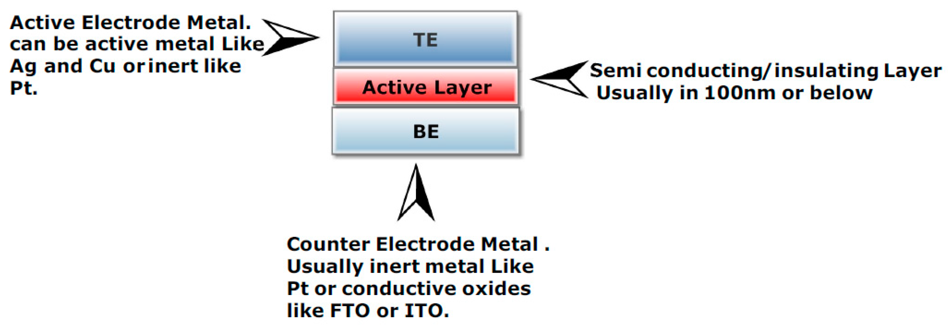
Abstract
1. Introduction
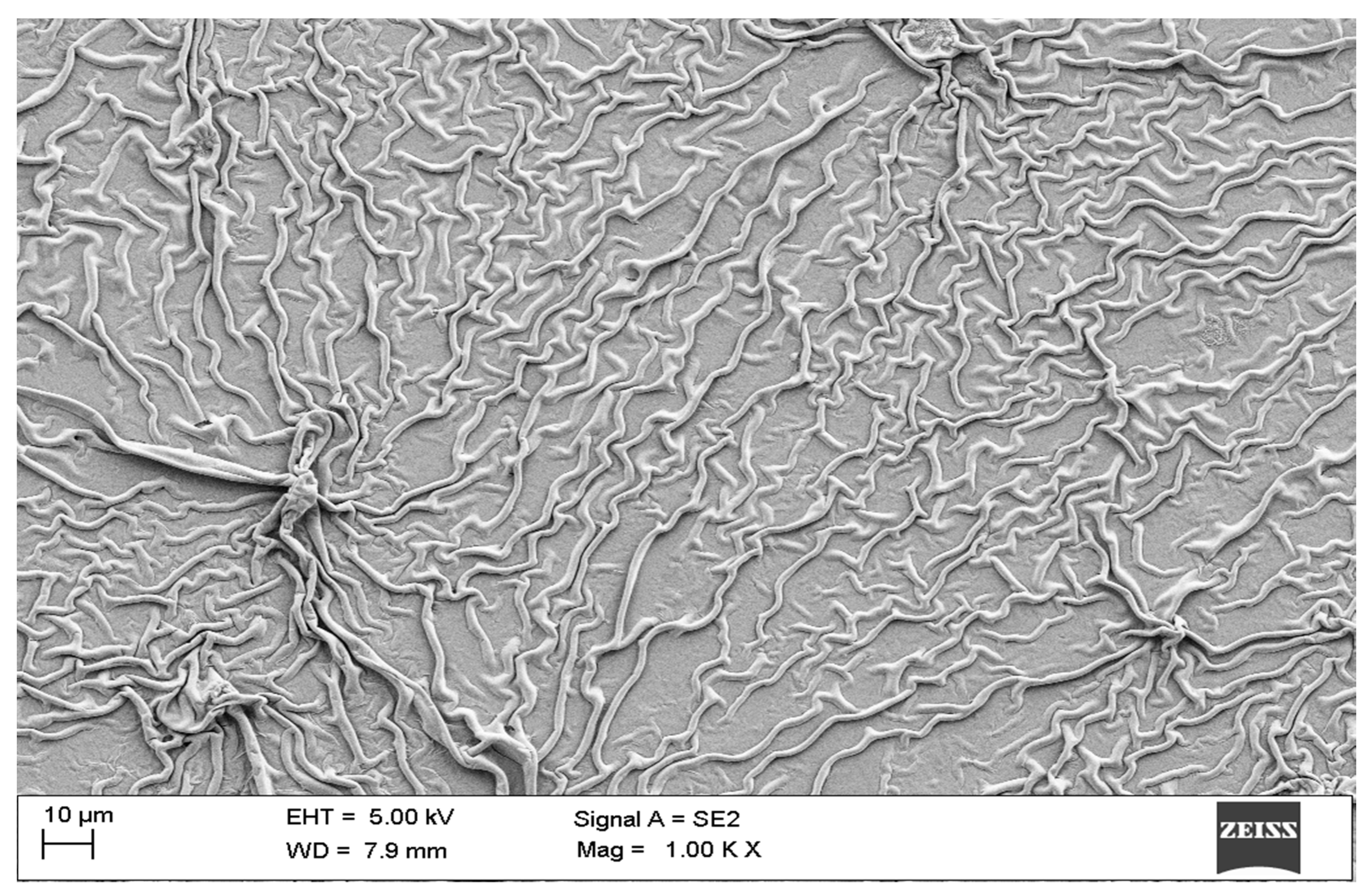
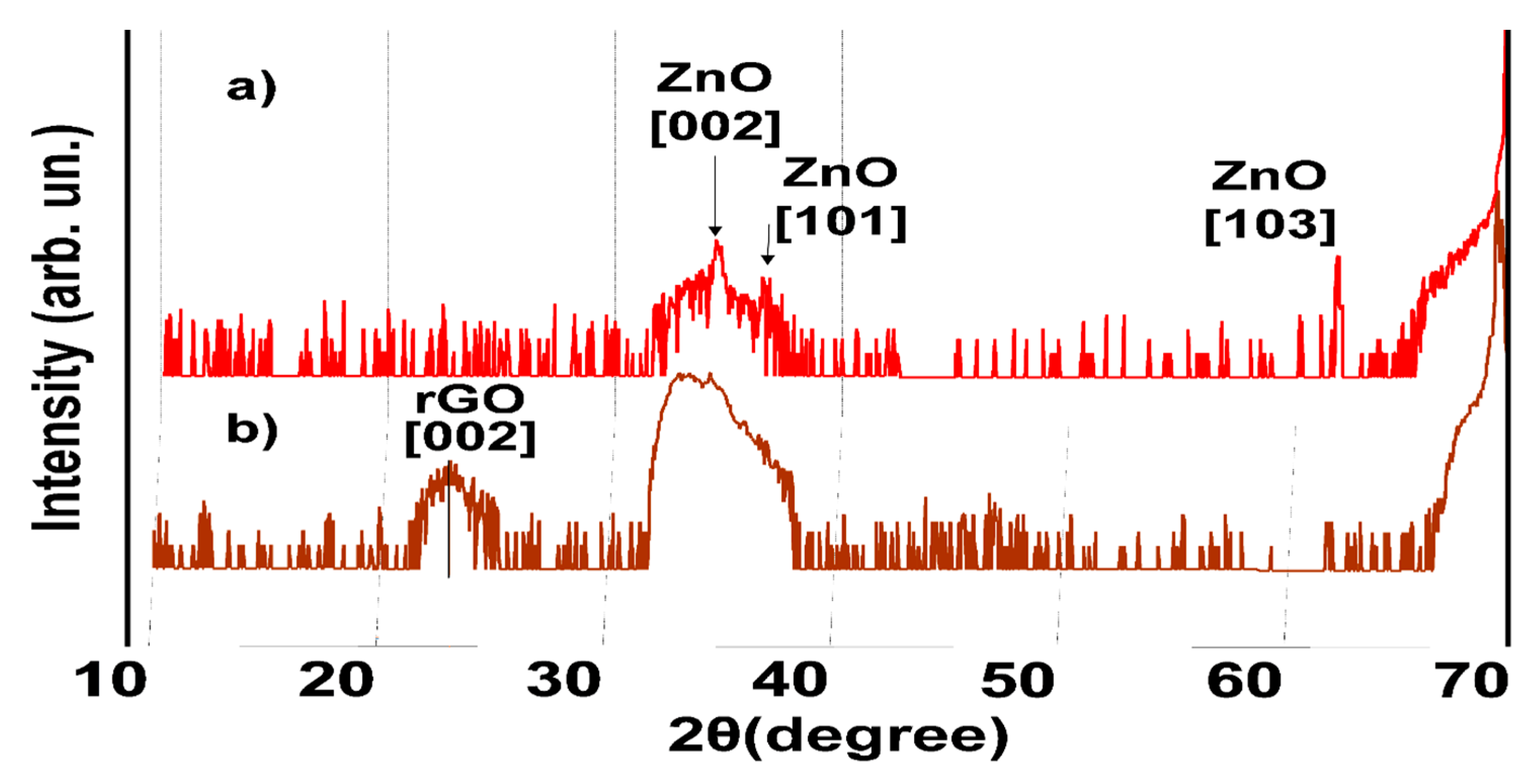
2. Materials and Methods
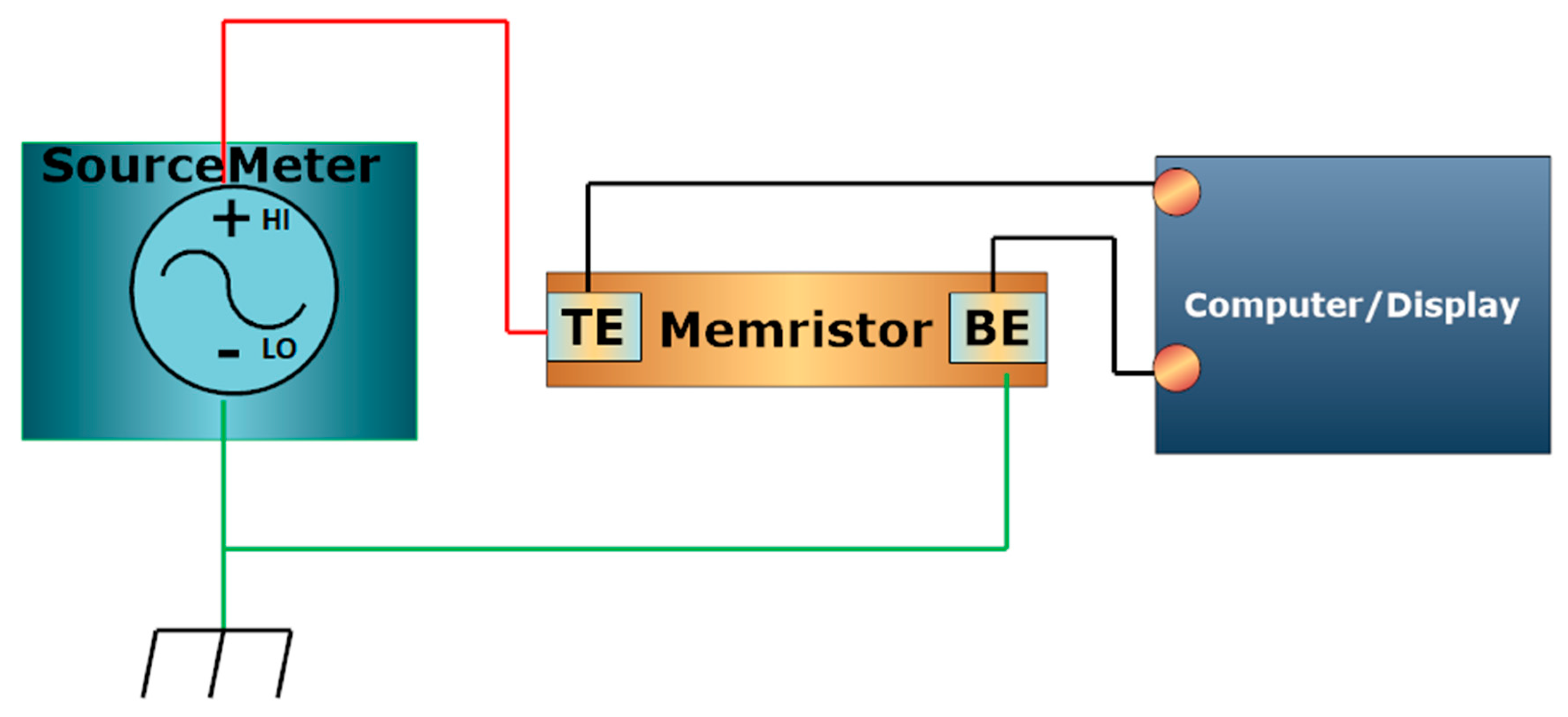
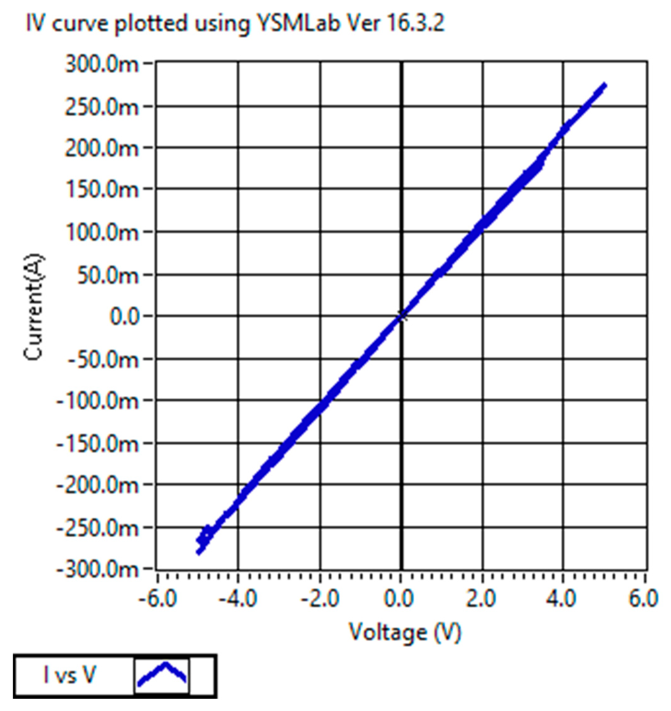
3. Electrical Characterization
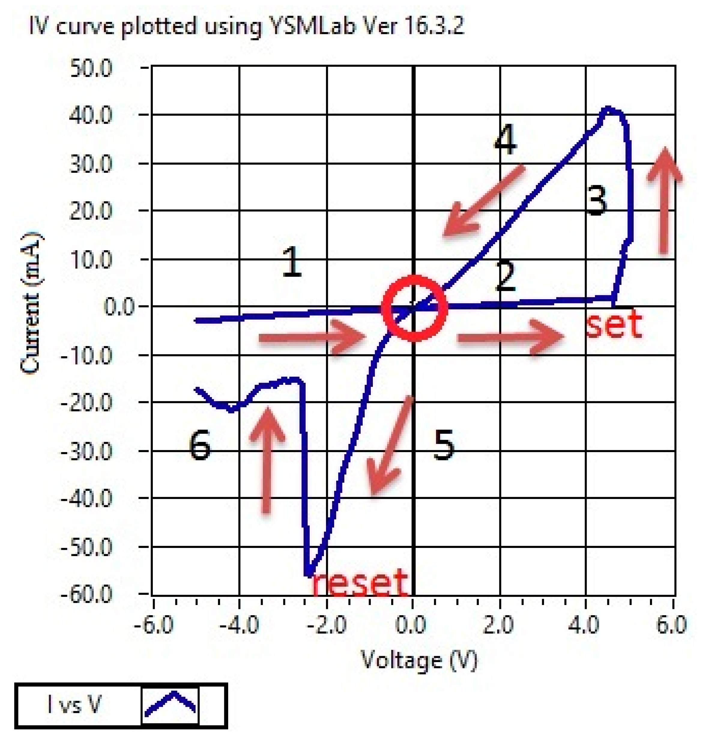
- The source meter starts to increase the voltage from −5 V toward 0 V, and the output current is very small.
- After passing 0 V, the output current starts to increase linearly.
- At Vset = +4.5 V, the device switches to the low resistive state (LRS), and after 4.5 V, the output current increases sharply (up to 5 V).
- Voltage starts reducing from +5 V toward 0 V, and the output current decreases linearly.
- Then, the polarity of the input voltage (below 0 V toward −5 V) is changed, and the output current decreases sharply.
- At Vreset = −2.5 Vm, the device switches to a high resistive state (HRS).
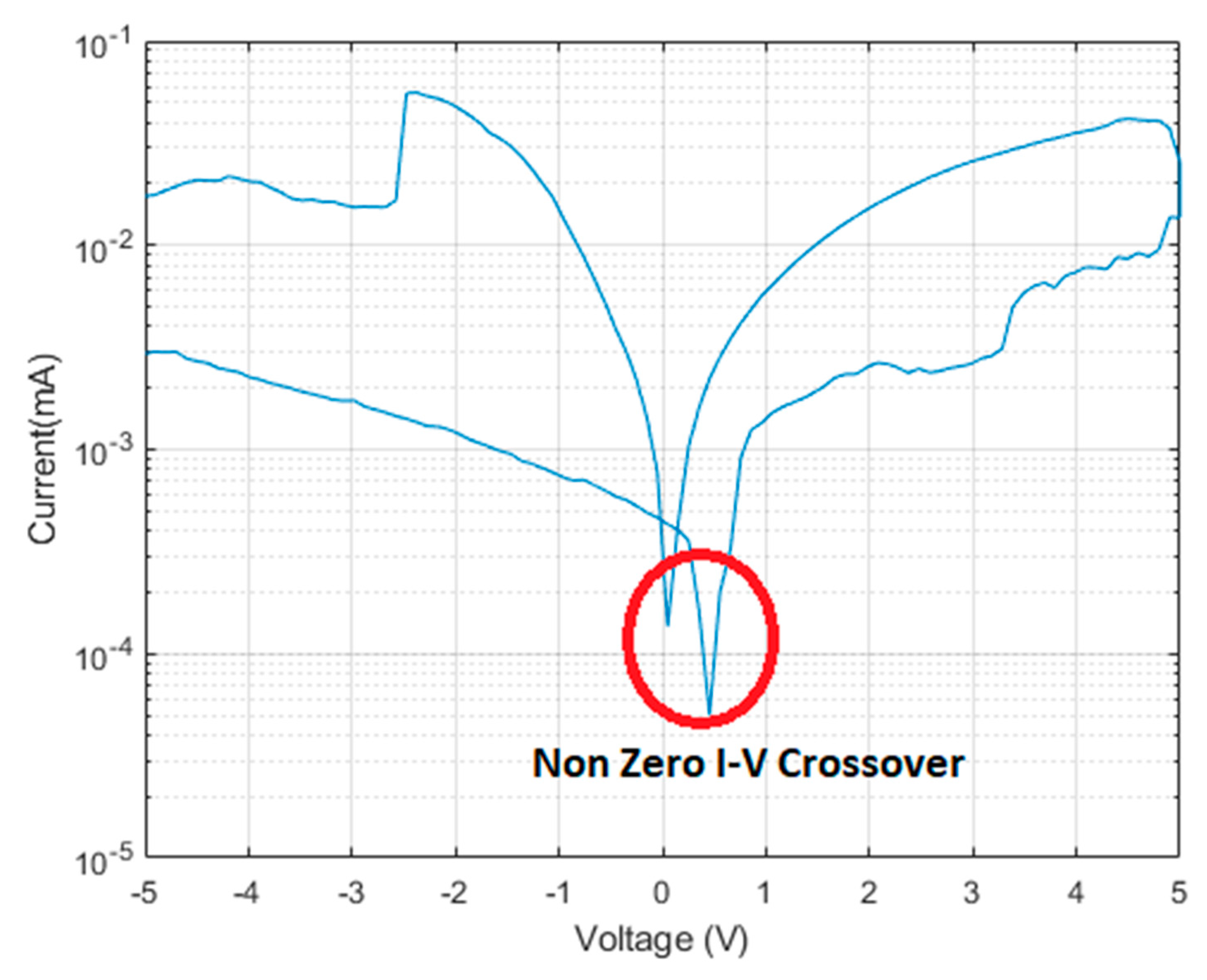
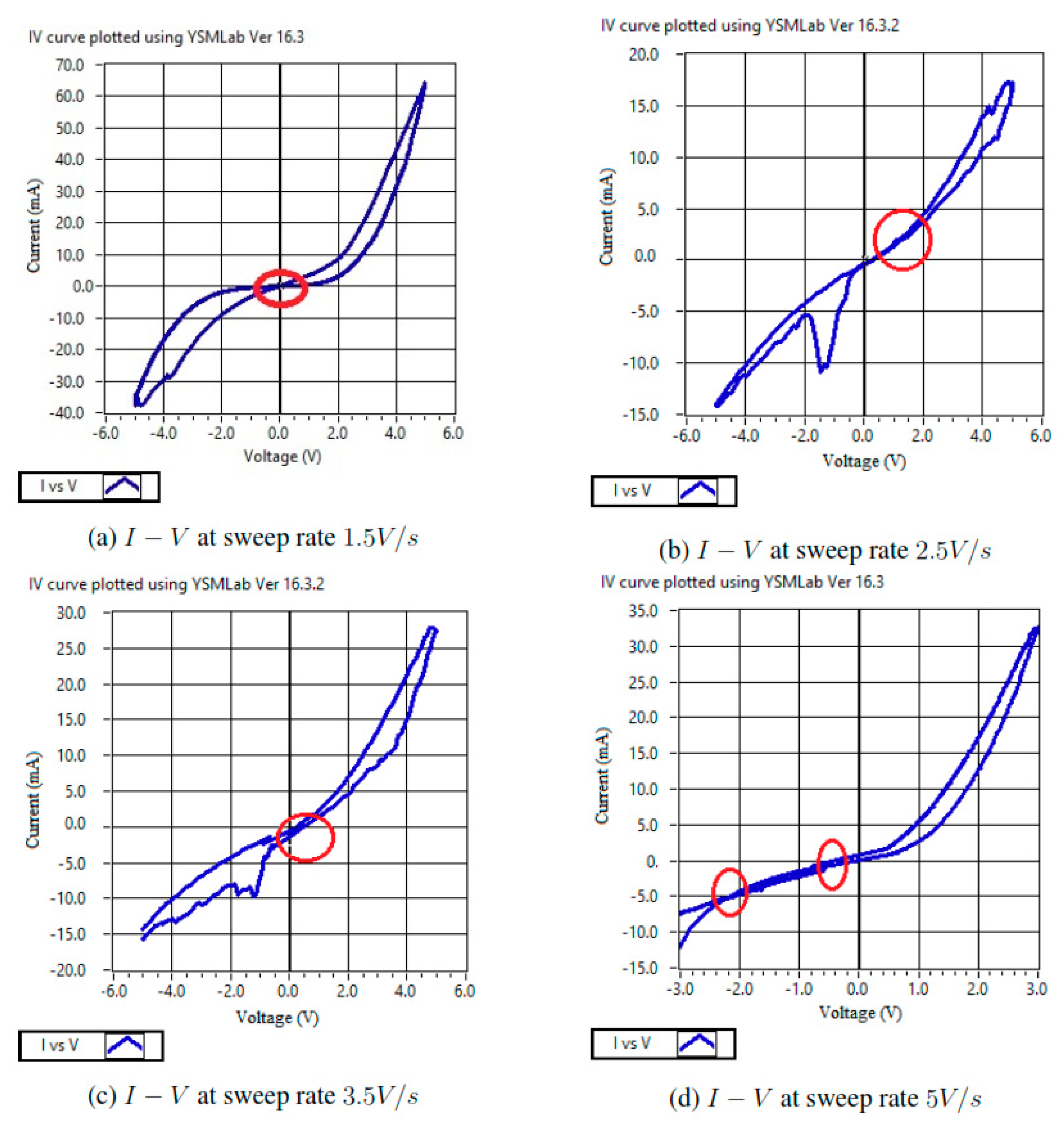
- With the increment in voltage sweep rate from 0.5 to 1.5 V/s (Figure 9a), the crossover point of the I–V curve shifts from the origin and moves slightly into the first quadrant of the I–V plane.
- With further increment in the sweep rate to 2.5 V/s, the I–V crossover point moves higher into the first quadrant (Figure 9b).
- 3.
- Continuing the increase in the voltage sweep rate from 2.5 to 3.5 V/s, the I–V crossover point now drifts down toward the third quadrant of the I–V plane (Figure 9c).
- 4.
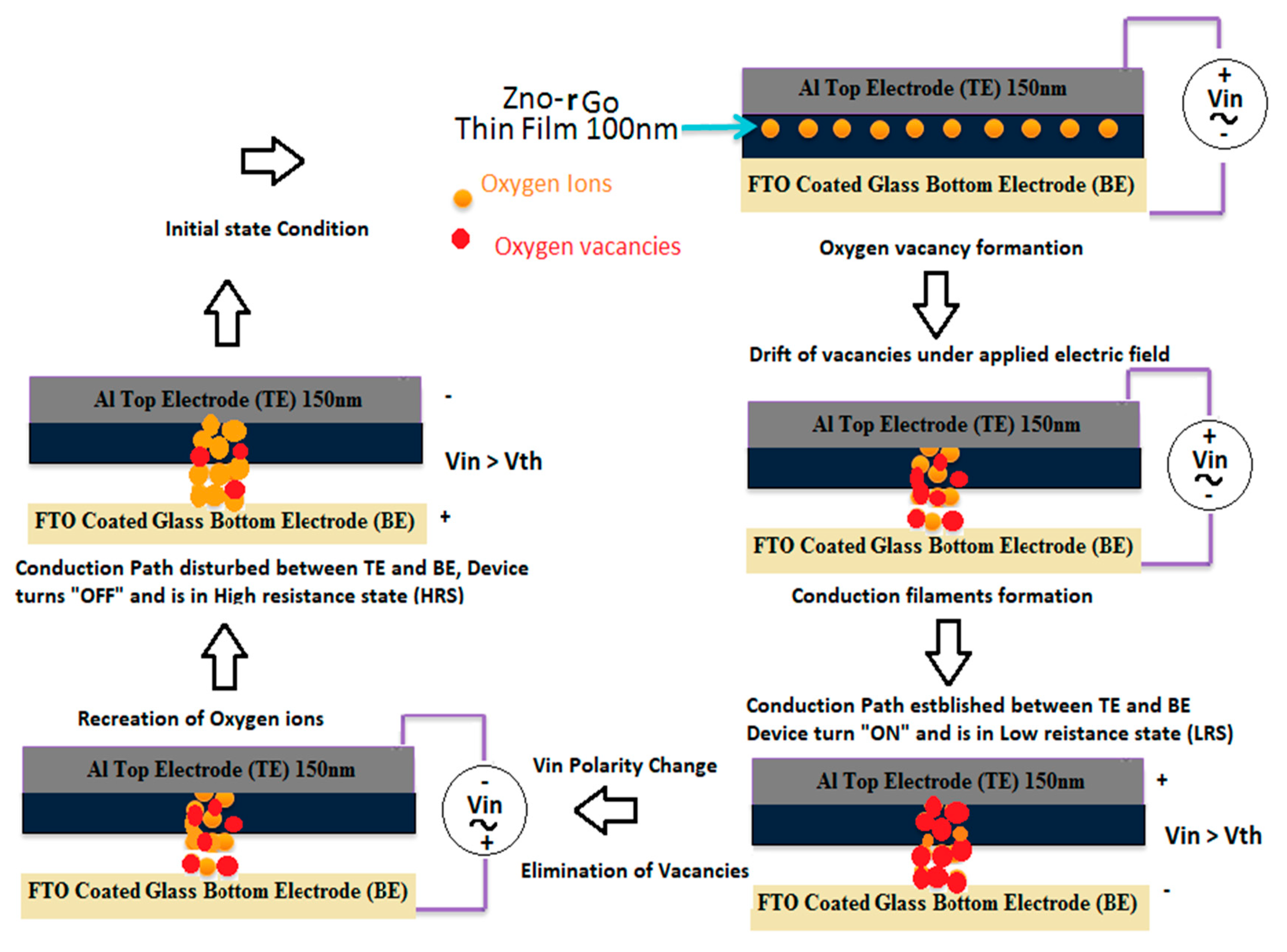
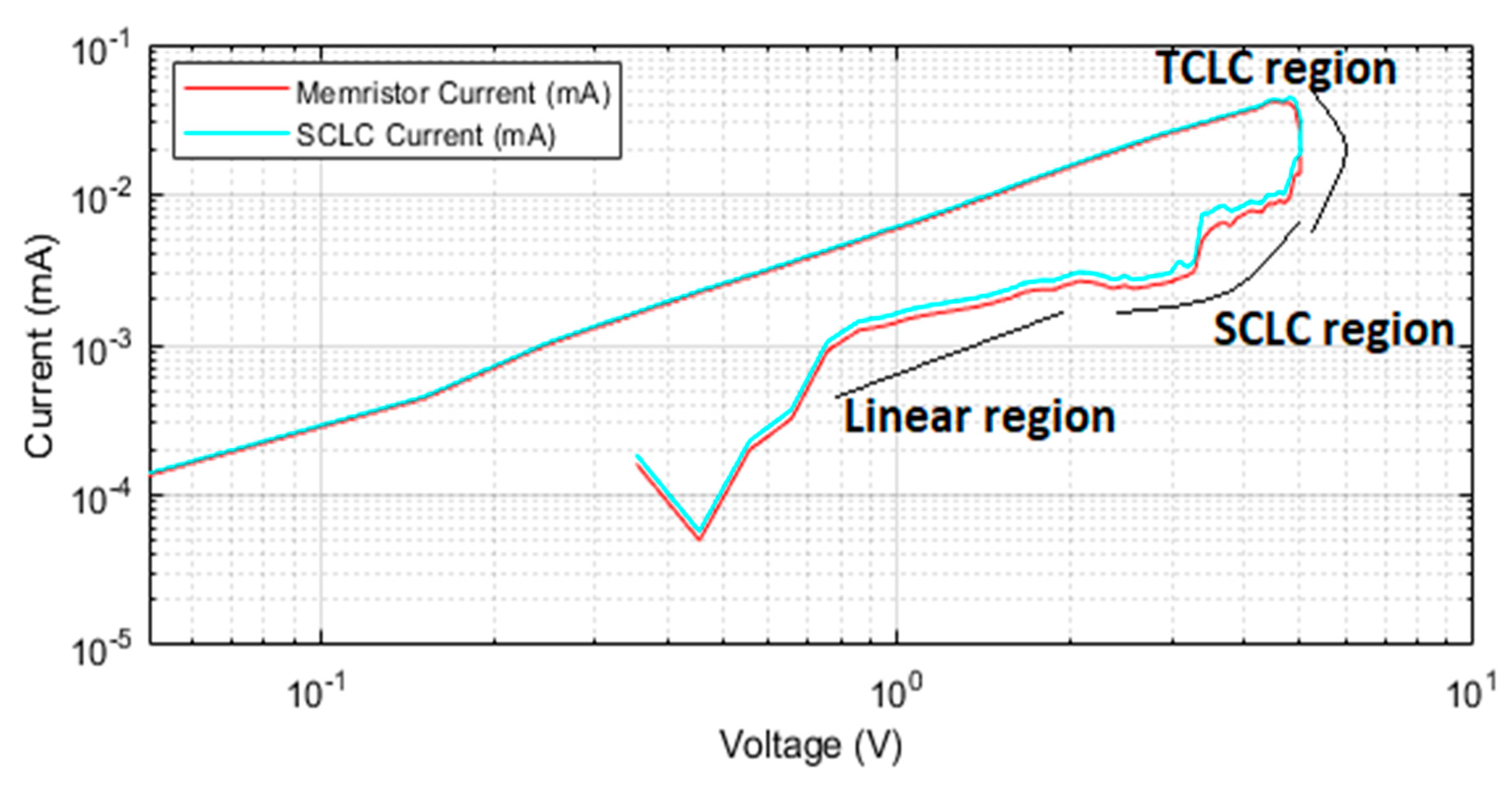
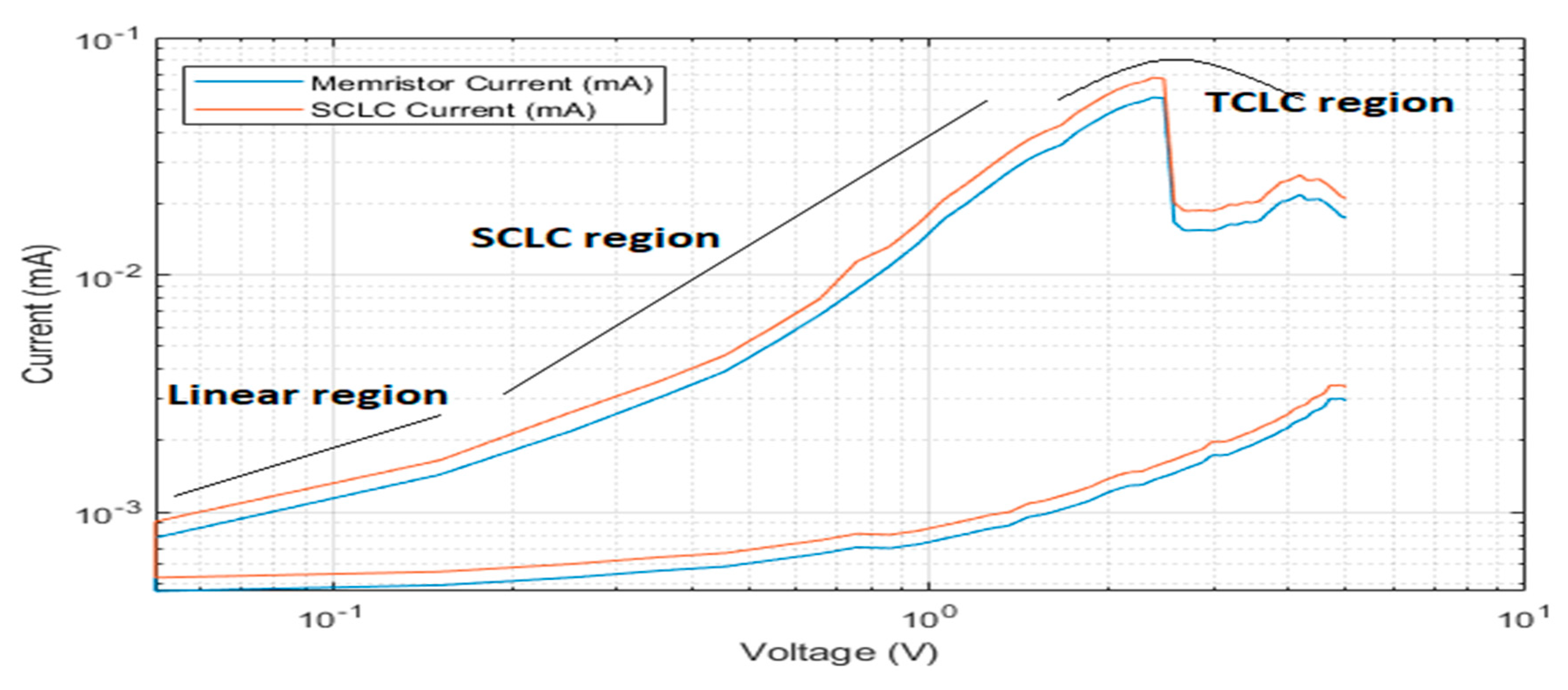
4. Resistive Switching Mechanism
5. Results and Discussion
6. Conclusions
Author Contributions
Funding
Acknowledgments
Conflicts of Interest
References
- Patil, S.R.; Chougale, M.Y.; Rane, T.D.; Khot, S.S.; Patil, A.A.; Bagal, O.S.; Jadhav, S.D.; Sheikh, A.D.; Kim, S.; Dongale, T.D. Solution-Processable ZnO Thin Film Memristive Device for Resistive Random Access Memory Application. Electronics 2018, 7, 445. [Google Scholar] [CrossRef]
- Cheng, T.; Rao, J.; Tang, X.; Yang, L.; Liu, N. Analog Memristive Characteristics and Conditioned Reflex Study Based on Au/ZnO/ITO Devices. Electronics 2018, 7, 141. [Google Scholar] [CrossRef]
- Zhao, X.; Li, Y.; Ai, C.; Wen, D. Resistive Switching Characteristics of Li-Doped ZnO Thin Films Based on Magnetron Sputtering Materials. Materials 2019, 12, 1282. [Google Scholar] [CrossRef] [PubMed]
- Simanjuntak, F.M.; Panda, D.; Wei, K.H.; Tseng, T.Y. Status and Prospects of ZnO-Based Resistive Switching Memory Devices. Nanoscale Res. Lett. 2016, 11, 368. [Google Scholar] [CrossRef] [PubMed]
- Romero, F.J.; Toral-Lopez, A.; Ohata, A.; Morales, D.P.; Ruiz, F.G.; Godoy, A.; Rodriguez, N. Laser-Fabricated Reduced Graphene Oxide Memristors. Nanomaterials 2019, 9, 897. [Google Scholar] [CrossRef] [PubMed]
- Lian, X.; Shen, X.; Lu, L.; He, N.; Wan, X.; Samanta, S.; Tong, Y. Resistance Switching Statistics and Mechanisms of Pt Dispersed Silicon Oxide-Based Memristors. Micromachines 2019, 10, 369. [Google Scholar] [CrossRef] [PubMed]
- Villena, M.A.; Roldán, J.B.; González, M.B.; González-Rodelas, P.; Jiménez-Molinos, F.; Campabadal, F.; Barrera, D. A new parameter to characterize the charge transport regime in Ni/HfO2/Si-n+-based RRAMs. Solid-State Electron. 2016, 118, 56–60. [Google Scholar] [CrossRef]
- Zamarreño-Ramos, C.; Camuñas-Mesa, L.A.; Pérez-Carrasco, J.A.; Masquelier, T.; Serrano-Gotarredona, T.; Linares-Barranco, B. On spike-timing-dependent plasticity, memristive devices, and building a self-learning visual cortex. Front. Neurosci. 2011, 5, 26. [Google Scholar] [CrossRef]
- Khanal, G.M.; Acciarito, S.; Cardarilli, G.C.; Chakraborty, A.; Nunzio, L.D.; Fazzolari, R.; Cristini, A.; Re, M.; Susi, G. Synaptic behavior in ZnO-rGO composites thin film memristor. Electron. Lett. 2017, 53, 296–298. [Google Scholar] [CrossRef]
- Bi, G.-Q.; Poo, M.-M. Synaptic modifications in cultured hippocampal neurons: Dependence on spike timing, synaptic strength, and postsynaptic cell type. J. Neurosci. 1998, 18, 10464–10472. [Google Scholar] [CrossRef]
- Likharev, K.K. Cross nets: Neuromorphic hybrid cmos/nano electronic networks. Sci. Adv. Mater. 2011, 3, 322–331. [Google Scholar] [CrossRef]
- Indiveri, G.; Linares-Barranco, B.; Hamilton, T.J.; van Schaik, A.; Etienne-Cummings, R.; Delbruck, T.; Liu, S.-C.; Dudek, P.; Häfliger, P.; Renaud, S.; et al. Neuromorphic silicon neuron circuits. Front. Neurosci. 2011, 5, 73. [Google Scholar] [CrossRef] [PubMed]
- Serrano-Gotarredona, T.; Masquelier, T.; Prodromakis, T.; Indiveri, G.; Linares-Barranco, B. STDP and STDP variations with memristors for spiking neuromorphic learning systems. Front. Neurosci. 2013, 7, 2. [Google Scholar] [CrossRef] [PubMed]
- Snider, G.S. Spike-timing-dependent learning in memristive nanodevices. In Proceedings of the IEEE International Symposium on Nanoscale Architectures, Anaheim, CA, USA, 12–13 June 2008; pp. 85–92. [Google Scholar] [CrossRef]
- Acciarito, S.; Cristini, A.; Nunzio, L.D.; Khanal, G.M.; Susi, G. An avlsi driving circuit for memristor-based stdp. In Proceedings of the 12th Conference on Ph.D. Research in Microelectronics and Electronics (PRIME), Lisbon, Portugal, 27–30 June 2016. [Google Scholar] [CrossRef]
- Chua, L.O. Memristor—The missing circuit element. IEEE Trans. Circuit Theory 1971, 18, 507–519. [Google Scholar] [CrossRef]
- Di Ventra, M.; Pershin, Y.V.; Chua, L.O. Circuit elements with memory: Memristors, memcapacitors, and meminductors. Proc. IEEE 2009, 97, 1717–1724. [Google Scholar] [CrossRef]
- Chua, L.O.; Kang, S.M. Memristive devices and systems. Proc. IEEE. 1976, 64, 209–223. [Google Scholar] [CrossRef]
- Li, L.; Zhang, Y.; Chew, Z. A Cu-ZnO nanowire-Cu resistive switching device. Nano-Micro Lett. 2013, 5, 159–162. [Google Scholar] [CrossRef]
- Qingjiang, L.; Khiat, A.; Salaoru, I.; Papavassiliou, C.; Hui, X.; Prodromakis, T. Memory impedance in TiO2 based metal-insulator-metal devices. Sci. Rep. 2014, 4, 4522. [Google Scholar] [CrossRef]
- Valov, I.; Linn, E.; Tappertzhofen, S.; Schmelzer, S.; van den Hurk, J.; Lentz, F.; Waser, R. Nanobatteries in redox-based resistive switches require extension of memristor theory. Nat. Commun. 2013, 4, 1771. [Google Scholar] [CrossRef]
- Khanal, G.M.; Cardarilli, G.C.; Chakraborty, A.; Acciarito, S.; Mulla, M.Y.; Nunzio, L.D.; Fazzolari, R.; Re, M. A ZnO/rGO composite thin film discrete memristor. In Proceedings of the 2016 IEEE International Conference on Semiconductor Electronics (ICSE) (IEEE-ICSE2016), Kuala Lumpur, Malaysia, 17–19 August 2016. [Google Scholar] [CrossRef]
- Song, J.; Zhang, Y.; Xu, C.; Wu, W.; Wang, Z.L. Polar charges induced electric hysteresis of ZnO nano/microwire for fast data storage. Nano Lett. 2011, 11, 2829–2834. [Google Scholar] [CrossRef]
- Sarma, S.; Mothudi, B.M.; Dhlamini, M.S. Observed coexistence of memristive, memcapacitive and meminductive characteristics in polyvinyl alcohol/cadmium sulphide nano composites. J. Mater. Sci. Mater. Electron. 2016, 27, 4551–4558. [Google Scholar] [CrossRef]
- Lewis, D.L.; Lee, H.-H.S. Architectural evaluation of 3D stacked ReRam caches. In Proceedings of the IEEE International Conference on 3D System Integration, San Francisco, CA, USA, 28–30 September 2009; pp. 1–4. [Google Scholar] [CrossRef]
- Kudithipudi, D.; Merkel, C.E. Reconfigurable memristor fabrics for heterogeneous computing. In Advances in Neuromorphic Memristor Science and Applications; Springer: Dordrecht, The Netherlands, 2012; pp. 89–106. [Google Scholar] [CrossRef]
- Macaluso, R.; Mosca, M.; Costanza, V.; D’angelo, A.; Lullo, G.; Caruso, F.; Calì, C.; DiFranco, F.; Santamaria, M.; DiQuarto, F. Resistive switching behaviour in ZnO and VO2 memristors grown by pulsed laser deposition. Electron. Lett. 2014, 50, 262–263. [Google Scholar] [CrossRef]
- Kumar, A.; Rawal, Y.; Baghini, M.S. Fabrication and characterization of the ZnO-based memristor. In Proceedings of the IEEE International Conference on Emerging Electronics, Mumbai, India, 15–17 December 2012; pp. 1–3. [Google Scholar] [CrossRef]
- Sekhar, K.C.; Kamakshi, K.; Bernstorff, S.; Gomes, M.J.M. Effect of annealing temperature on photoluminescence and resistive switching characteristics of ZnO/Al2O3 multilayer nanostructures. J. Alloys Compd. 2015, 619, 248–252. [Google Scholar] [CrossRef]
- Sawa, A. Resistive switching in transition metal oxides. Mater. Today 2008, 11, 28–36. [Google Scholar] [CrossRef]
- Yang, Y.C.; Pan, F.; Zeng, F.; Liu, M. Switching mechanism transition induced by annealing treatment in nonvolatile Cu/ZnO/Cu/ZnO/Pt resistive memory: From carrier trapping/detrapping to electrochemical metallization. J. Appl. Phys. 2009, 106, 123705. [Google Scholar] [CrossRef]
- Chakraborty, A.; Khanal, G.M. Study of sol-gel based synthesized ZnO-rGO composite thin film. In Proceedings of the NGPT Conference, Rome, Italy, 15–17 June 2016. [Google Scholar]
- Chakraborty, A.; Pizzoferrato, R.; Agresti, A.; de Matteis, F.; Orsini, A.; Medaglia, P.G. Wet-chemical synthesis of ZnO nanowires on low-temperature photo-activated ZnO-rGO composite thin film with enhanced photoconduction. J. Electron. Mater. 2018, 47, 5863–5869. [Google Scholar] [CrossRef]
- Scherer, G.W. Sintering of sol-gel films. J. Sol-Gel Sci. Technol. 1997, 8, 353–363. [Google Scholar] [CrossRef]
- Kwon, S.J.; Park, J.H.; Park, J.-G. Wrinkling of a sol-gel-derived thin film. Phys. Rev. E 2005, 71, 011604. [Google Scholar] [CrossRef]
- Uddin, A.S.M.I.; Phan, D.T.; Chung, G.S. Synthesis of ZnO nanoparticles-reduced graphene oxide composites and their intrinsic gas sensing properties. Surf. Rev. Lett. 2014, 21, 1450086. [Google Scholar] [CrossRef]
- Chua, L. Everything you wish to know about memristors but are afraid to ask. Radioengineering 2015, 24, 319–368. [Google Scholar] [CrossRef]
- Biolek, D.; Biolek, Z.; Biolkova, V.; Ascoli, A.; Tetzlaff, R. About v-i Pinched Hysteresis of Some Non-Memristive Systems. Math. Probl. Eng. 2018, 2018, 1747865. [Google Scholar] [CrossRef]
- Mouttet, B. Memresistors and non-memristive zero-crossing hysteresis curves. arXiv 2012, arXiv:1201.2626. [Google Scholar]
- Kamble, G.U.; Shetake, N.P.; Yadav, S.D.; Teli, A.M.; Patil, D.S.; Pawar, S.A.; Karanjkar, M.M.; Patil, P.S.; Shin, J.C.; Orlowski, M.K.; et al. Coexistence of filamentary and homogeneous resistive switching with memristive and meminductive memory effects in Al/MnO2/SS thin film metal–insulator–metal device. Int. Nano Lett. 2018, 8, 263. [Google Scholar] [CrossRef]
- Dongale, T.D.; Khot, K.V.; Mali, S.S.; Patil, P.S.; Gaikwad, P.K.; Kamat, R.K.; Bhosale, P.N. Development of Ag/ZnO/FTO thin film memristor using aqueous chemical route. Mater. Sci. Semicond. Process. 2015, 40, 523–526. [Google Scholar] [CrossRef]
- Chew, Z.J.; Li, L. A discrete memristor made of ZnO nanowires synthesized on printed circuit board. Mater. Lett. 2013, 91, 298–300. [Google Scholar] [CrossRef]
- Gul, F.; Efeoglu, H. Bipolar resistive switching and conduction mechanism of an Al/ZnO/Al-based memristor. Superlattices Microstruct. 2017, 101, 172–179. [Google Scholar] [CrossRef]
- Tan, C.; Liu, Z.; Huang, W.; Zhang, H. Non-volatile resistive memory devices based on solution-processed ultrathin two-dimensional nanomaterials. Chem. Soc. Rev. 2015, 44, 2615–2628. [Google Scholar] [CrossRef]
- Yang, J.J.; Borghetti, J.; Murphy, D.; Stewart, D.R.; Williams, R.S. A Family of Electronically Reconfigurable Nanodevices. Adv. Mater. 2009, 21, 3754–3758. [Google Scholar] [CrossRef]
- Pan, F.; Gao, S.; Chen, C.; Song, C.; Zeng, F. Recent progress in resistive random-access memories: Materials, switching mechanisms, and performance. Mater. Sci. Eng. R Rep. 2014, 83, 1–59. [Google Scholar] [CrossRef]
- Miao, F.; Yi, W.; Goldfarb, I.; Yang, J.J.; Zhang, M.X.; Pickett, M.D.; Strachan, J.P.; Ribeiro, G.M.; Williams, R.S. Continuous electrical tuning of the chemical composition of TaO(x)-based memristors. ACS Nano 2012, 6, 2312–2318. [Google Scholar] [CrossRef]
- Sun, Y.; Yan, X.; Zheng, X.; Liu, Y.; Zhao, Y.; Shen, Y.; Liao, Q.; Zhang, Y. High on–off ratio improvement of ZnO based forming-free memristor by surface hydrogen annealing. ACS Appl. Mater. Interfaces 2015, 7, 7382–7388. [Google Scholar] [CrossRef] [PubMed]
- Gale, E.; Pearson, D.; Kitson, S.; Adamatzky, A.; de Lacy Costello, B. The effect of changing electrode metal on solution-processed flexible titanium dioxide memristors. Mater. Chem. Phys. 2015, 162, 20–30. [Google Scholar] [CrossRef]
- Sai, N.; Bushong, N.; Hatcher, R.; di Ventra, M. Microscopic current dynamics in nanoscale junctions. Phys. Rev. B 2007, 75, 115410. [Google Scholar] [CrossRef]
- Kim, T.H.; Jang, E.Y.; Lee, N.J.; Choi, D.J.; Lee, K.J.; Jang, J.T.; Choi, J.S.; Moon, S.H.; Cheon, J. Nanoparticle assemblies as memristors. Nano Lett. 2009, 9, 2229–2233. [Google Scholar] [CrossRef]
- Yang, Y.C.; Pan, F.; Liu, Q.; Liu, M.; Zeng, F. Fully room-temperature-fabricated nonvolatile resistive memory for ultrafast and high-density memory application. Nano Lett. 2009, 9, 1636–1643. [Google Scholar] [CrossRef]
- Huang, Y.; Luo, Y.; Shen, Z.; Yuan, G.; Zeng, H. Unipolar resistive switching of ZnO-single-wire memristors. Nanoscale Res. Lett 2014, 9, 381. [Google Scholar] [CrossRef]
- Lampert, M.A. Simplified theory of space-charge-limited currents in an insulator with traps. Phys. Rev. 1956, 103, 1648–1656. [Google Scholar] [CrossRef]
- Mouttet, B. A Memadmittance Systems Model for Thin Film Memory Materials. arXiv 2010, arXiv:1003.2842. [Google Scholar]


© 2020 by the authors. Licensee MDPI, Basel, Switzerland. This article is an open access article distributed under the terms and conditions of the Creative Commons Attribution (CC BY) license (http://creativecommons.org/licenses/by/4.0/).
Share and Cite
Cardarilli, G.C.; Khanal, G.M.; Di Nunzio, L.; Re, M.; Fazzolari, R.; Kumar, R. Memristive and Memory Impedance Behavior in a Photo-Annealed ZnO–rGO Thin-Film Device. Electronics 2020, 9, 287. https://doi.org/10.3390/electronics9020287
Cardarilli GC, Khanal GM, Di Nunzio L, Re M, Fazzolari R, Kumar R. Memristive and Memory Impedance Behavior in a Photo-Annealed ZnO–rGO Thin-Film Device. Electronics. 2020; 9(2):287. https://doi.org/10.3390/electronics9020287
Chicago/Turabian StyleCardarilli, Gian Carlo, Gaurav Mani Khanal, Luca Di Nunzio, Marco Re, Rocco Fazzolari, and Raj Kumar. 2020. "Memristive and Memory Impedance Behavior in a Photo-Annealed ZnO–rGO Thin-Film Device" Electronics 9, no. 2: 287. https://doi.org/10.3390/electronics9020287
APA StyleCardarilli, G. C., Khanal, G. M., Di Nunzio, L., Re, M., Fazzolari, R., & Kumar, R. (2020). Memristive and Memory Impedance Behavior in a Photo-Annealed ZnO–rGO Thin-Film Device. Electronics, 9(2), 287. https://doi.org/10.3390/electronics9020287