Article

Bias Temperature Instability Aware and Soft Error Tolerant Radiation Hardened 10T SRAM Cell

Institute for Microelectronics, Technische Universität Wien, 1040 Vienna, Austria
*
Author to whom correspondence should be addressed.
Electronics 2020, 9(2), 256; https://doi.org/10.3390/electronics9020256
Submission received: 3 December 2019 / Revised: 16 January 2020 / Accepted: 27 January 2020 / Published: 3 February 2020
(This article belongs to the Section Microelectronics)

Abstract

:
In this paper, we propose an asymmetric radiation-hardened 10T (AS10T) SRAM cell and analyze the impact of bias temperature instabilities (BTI) on the single event upset of the modified structure. For this, we make use of a read decoupled circuit to improve the stability of the reading cycle, and a charge booster circuit to increase the critical charge at the sensitive node of the SRAM cell. First, we compare the noise margin of several reference cells and can clearly observe that the read static noise margin (RSNM) of AS10T is 3.25× higher than as can be achieved for the 6T SRAM cell. This improvement is due to the read decoupled path used for the read operation. To analyze the soft-error hardening, we calculate the critical charge and observe that the critical charge of the proposed AS10T cell exceed the same parameter of other SRAM cells. Further, we perform critical charge simulations and stability analysis considering BTI and observe that the AS10T SRAM cell is also less affected by BTI as the reference cells.

1. Introduction

Due to rapid scaling of integrated devices and circuits, reliability issues have become more serious concerns in modern applications. Furthermore, with the scaling of the supply voltages, the node capacitance reduces, which makes the circuit susceptible to external noise caused by alpha particles and cosmic rays. The external noise sources can trigger a glitch at the sensitive nodes of a certain circuit, which gives rise to so-called transient faults. If such a fault occurs at the storage node of memory elements, it can alter the respective logic state, and a soft error can occur [1]. Soft errors due to radiations such as cosmic rays and alpha particles are a significant concern in modern CMOS technologies. SRAM cells are particularly susceptible to soft errors because the critical charge ( Q crit ) required to upset a cell is exceptionally small due to the typically low supply voltages, small noise margins, and lower node capacitances [2]. Next to soft errors, the performance of single MOS devices used in SRAM cells are additionally affected by aging mechanisms, which typically have a detrimental impact on the stability of SRAM cells. The primary aging mechanisms for modern integrated devices are the so called bias temperature instabilities (BTI). BTI can be classified into positive BTI (PBTI) and negative BTI (NBTI), depending on whether a positive or a negative bias is applied at the gate of the transistors. Both, PBTI and NBTI can be observed for NMOS and PMOS transistors. In general, BTI affects the performance of MOS transistors when they are biased in strong inversion [3]. For instance, the absolute value of the threshold voltage of PMOS and NMOS transistors drifts towards larger values with the stress time, as shown in Figure 1 for 32 nm CMOS technology using HSPICE. As can be seen, the effect of NBTI in PMOS is more severe than PBTI in NMOS transistors. The observed increase of the threshold voltage of transistors can lead to a decrease of the stability SRAM cells, and can increase the overall delay of the circuit. Even a small variation of the threshold voltage can affect the noise margin of the SRAM cells.
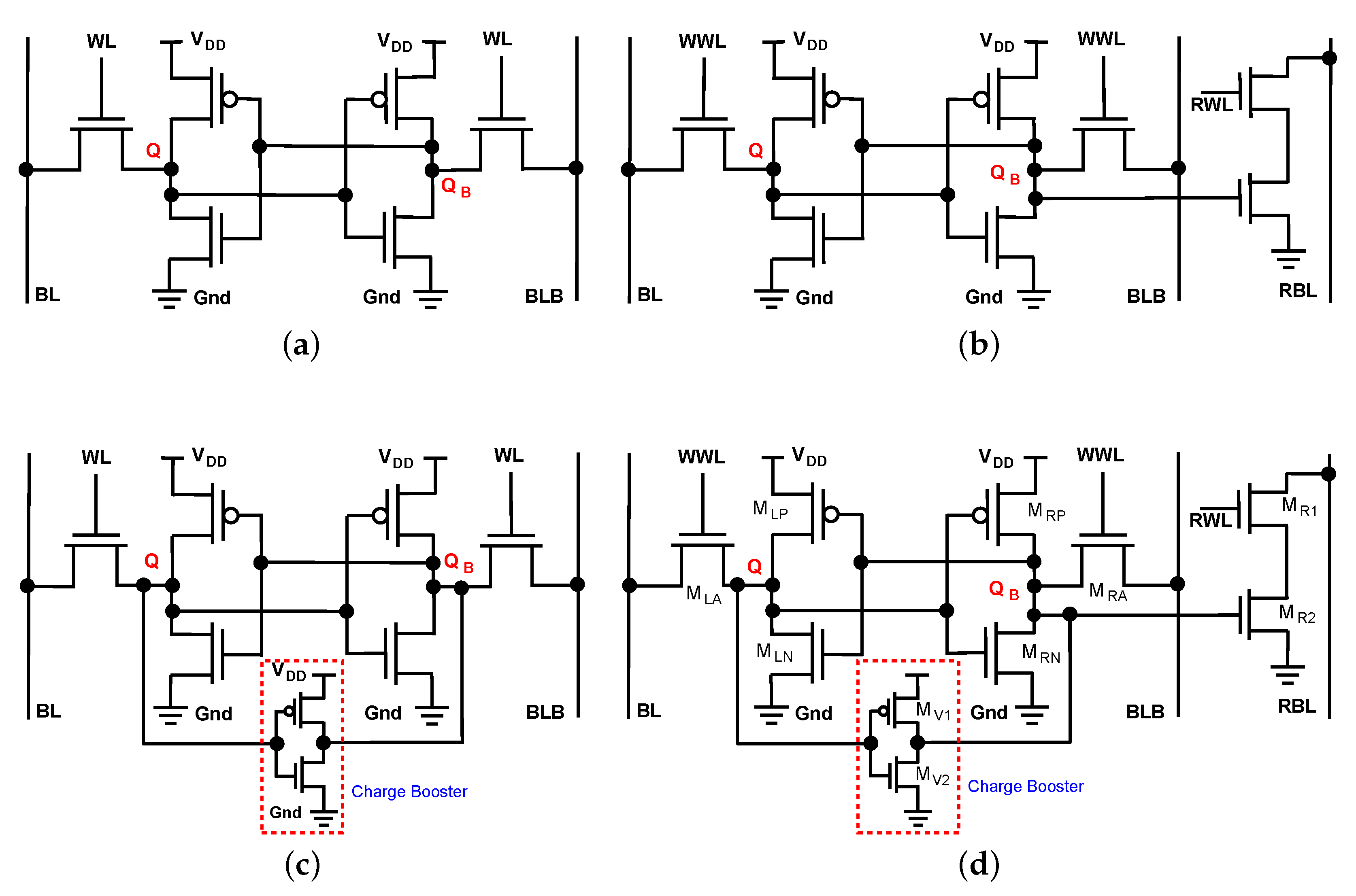
In recent investigations where the conventional 6T SRAM cell, as shown in Figure 2a, has been analyzed it has been observed that this cell does not provide adequate immunity against reliability issues, especially in harsh environments [2]. The 6T SRAM cell exhibits a reduced critical charge, which is not suitable for the applications where perturbations due to high energy particles are more likely.
To circumvent these limitations Chang et al. [4] proposed read decoupled 8T SRAM cell (RD8T) which requires separate write and read word-lines and bit-lines, as shown in Figure 2b. This cell improves the read static noise margin (RSNM) to be approximately equal to the hold static noise margin (SNM), without affecting other cell properties. The storage node capacitance of the RD8T SRAM cell remained the same as for the 6T SRAM cell. Although the read SNM was improved, the RD8T cell is still affected by external radiation at the same level of sensitivity as the 6T SRAM cell, thus no improvement in the soft error hardening could be achieved. In Reference [5], an asymmetric SRAM cell (AS8T) to improve soft error hardening is discussed. As shown in Figure 2c, a minimum sized charge booster is connected between the storage nodes to increase the node capacitance and thus to improve the soft error hardening. However, the read SNM of this SRAM cell remained at the same level as for the 6T SRAM cell. A pseudo-differential single event upset immune 12T (PD12T) SRAM cell is presented in Reference [6]. This cell exhibits soft error hardening but requires a large area. The we-Quatro circuit is one of the promising approaches providing robust operation under strongly radiative environment. However, the large area overhead might lead to higher write failure rate due to process variations [7]. A PPN based 10T SRAM cell with better performance is discussed in Reference [8], but its soft error tolerance has not been investigated so far. Based on the above discussions there is a high demand for optimization of the SRAM cells, to improve their soft error resilience as well as to improve the RSNM while avoiding to increase the required chip area, ensuring high signal integrity, and low power consumption of the SRAM cell.

2. Proposed Radiation Hardened Asymmetric 10T SRAM Cell

In this paper, an asymmetric radiation-hardened 10T (AS10T) SRAM cell is proposed, and the corresponding circuit is in Figure 2d. The AS10T SRAM cell is designed to improve the soft error performance at a minimum possible area overhead. To create the AS10T SRAM cell a minimum sized CMOS inverter ( M V 1 and M V 2 , named as charge booster) is placed between the storage nodes of the RD8T SRAM cell. The proposed design is inspired by the RD8T SRAM cell and is targeted to achieve an increased read SNM because of the separate read decoupled circuit ( M R 1 and M R 2 ) during read operation. Furthermore, the design is inspired by the AS8T SRAM cell to enhance the soft error hardening at the storage node by connecting a charge booster circuit. The newly proposed AS10T cell combines the advantage the RD8T and the AS8T SRAM cells. In the AS10T cell the role of the charge booster is to withstand the impact of particle strikes at the storage nodes of the SRAM cell. The charge booster increases the storage node capacitance and recovers the data by pulling back the correct logic state. The control signals for different operations of the proposed AS10T SRAM cell are given in Table 1. In the following the soft error hardening enhancement is thoroughly analyzed with consideration of the aging of MOS devices employing different SRAM cells as well as the proposed AS10T SRAM cell. The results reveal that the AS10T SRAM cell exhibits an overall enhanced soft error immunity because of an increased minimum amount of charge required to flip the stored data. The level of reliability in the proposed cell depends on the direction of the charge booster connection.
The highlights of this paper are as follows:
  • The charge booster circuit is added between the storage nodes which leads to a significant improvement of the critical charge of the cell.
  • The read decoupled circuit is introduced to improve the RSNM of the proposed SRAM cell.
  • A critical charge variation evaluation is discussed by considering different supply voltages and also temperature variation.
  • We analyze the effect of BTI on the stability of the previously mentioned SRAM cells.
  • Monte carlo simulations have been performed to analyze the effect of process variations on the considered cells.

3. Simulation Results and Discussion

To study the performance of circuits considering a radiation-hardened design in combination with the aging of semiconductor devices, we refer to the model already available for the PTM 32 nm CMOS technology [9]. The simulations are performed using Synopsis HSPICE [10] considering a supply voltage V dd = 0.9 V and the operating temperature is set to 25 °C, unless explicitly specified.

3.1. Stability Analysis

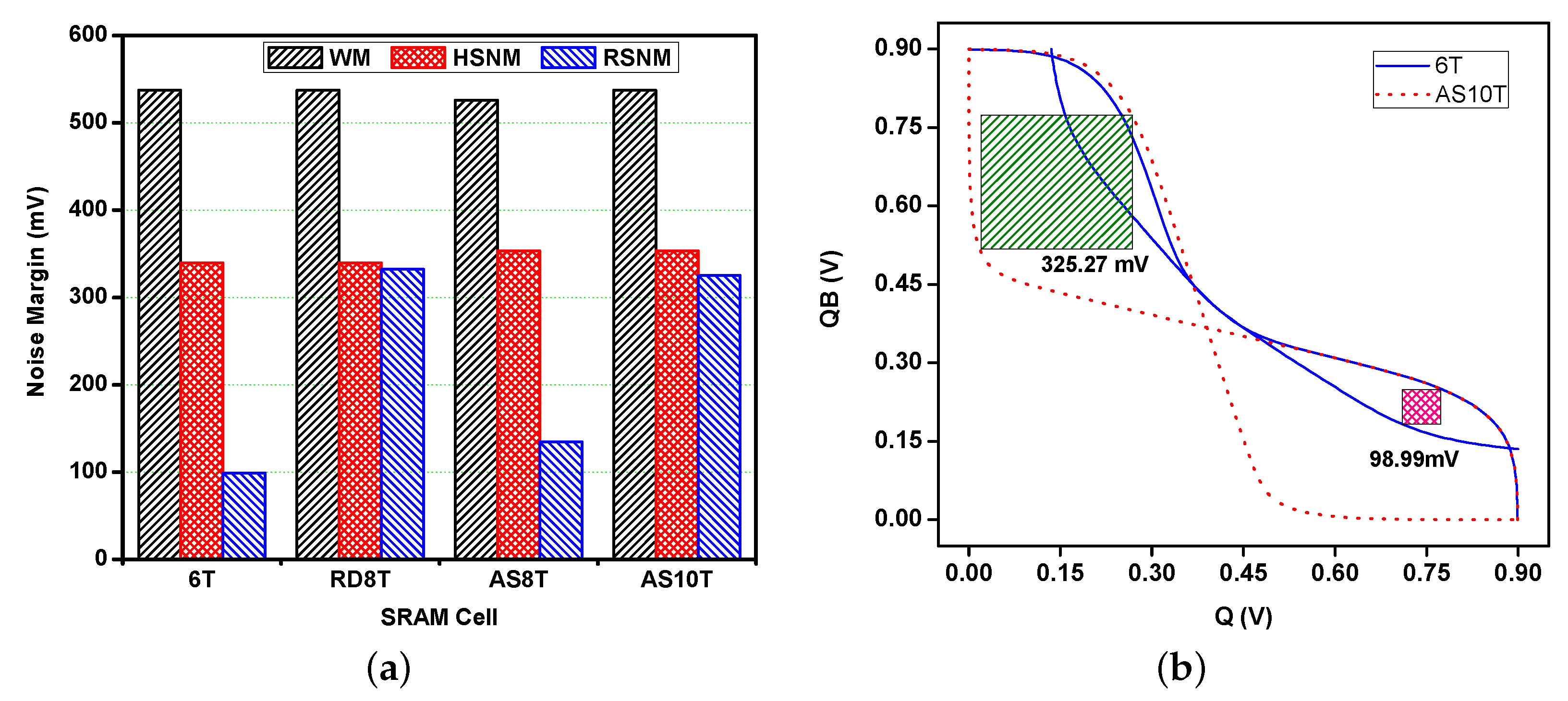
For the stability analysis of the previously mentioned SRAM cells, we have calculated the hold static noise margin (HSNM), the read static noise margin (RSNM), and the write margin (WM) at V dd = 0.9 V, as shown in Figure 3a. The stability is conventionally computed as the static noise margin. The noise margin is gauged by tracing the overlapped VTC (Butterfly diagram) for the back to back connected inverters which form the memory cell. The diagonal of the largest square that can fit in the eyes of the butterfly diagram finally determines the noise margin [8]. One can observe a similar WM for the 6T, RD8T, and AS10T SRAM cell, whereas the WM of AS8T is reduced by 2.1% compared to the others. The reduced write margin is due to the charge booster which is connected between the storage nodes, which strengthens the node by increasing the node capacitance. The HSNM of 6T and RD8T is the same because during hold operation the same transistor are active, whereas HSNM of AS8T and the AS10T is increased by 4.17% referred to 6T SRAM cell. This increase in HSNM of AS8T and AS10T is due to the presence of the charge booster connected between the storage nodes. One drawback of the 6T SRAM cell is its small RSNM. The read decoupled technique is one of the effective ways to increase RSNM because of the presence of a separate path during the read operation. The butterfly curve of 6T and AS10T is shown in Figure 3b, and clearly shows the RSNM of AS10T being higher than for the 6T SRAM cell. The RSNM of RD8T, AS8T, and AS10T is increased by 3.36×, 1.36×, and 3.29× compared to the 6T SRAM cell. The enhancement of the RSNM for RD8T and AS10T is due to the presence of a separate read decoupled path during read operation, whereas the RSNM for AS8T cell is high due to the charge booster circuit.

3.2. Critical Charge Analysis and Methodology

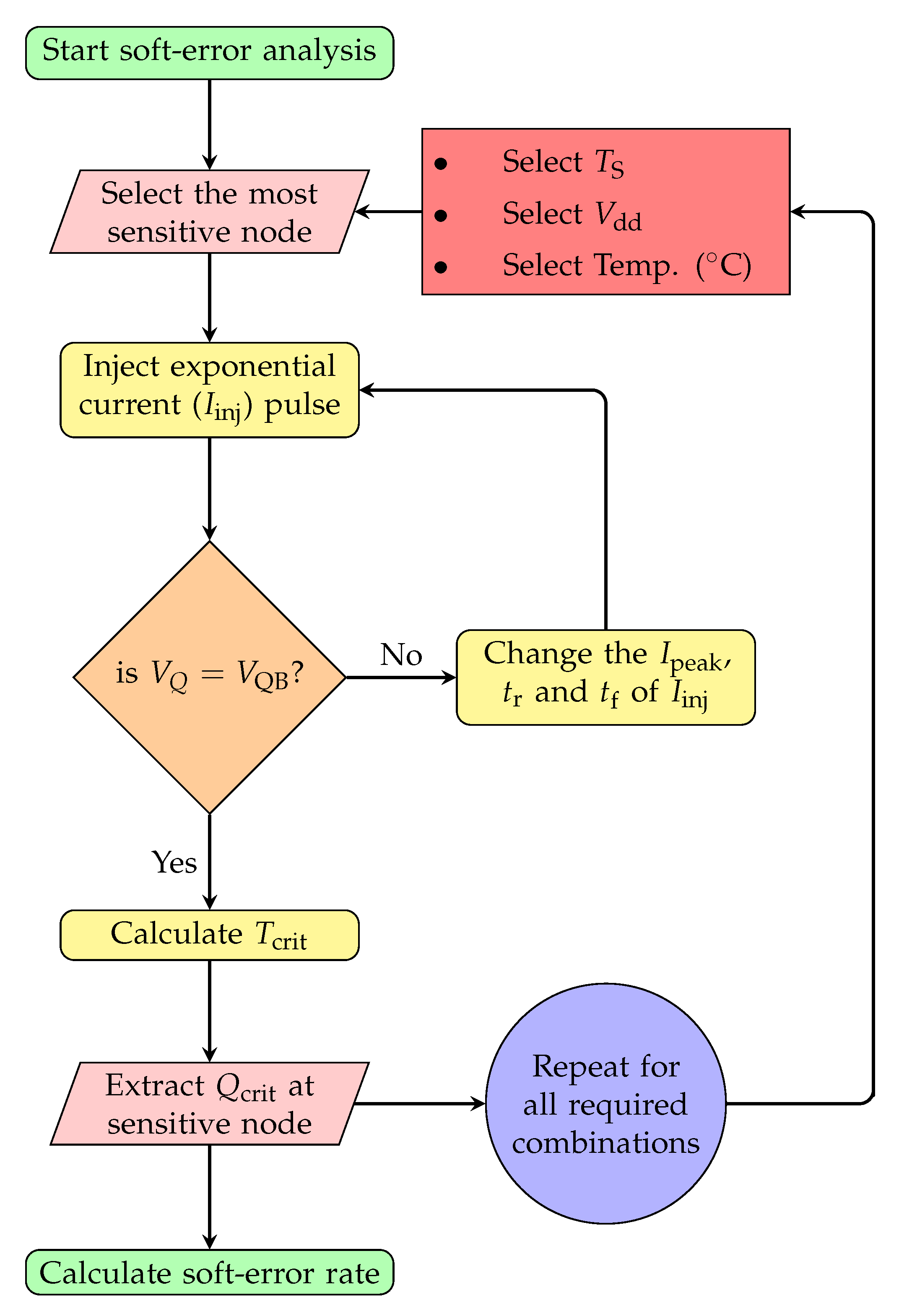
In order to investigate the radiation hardening using HSPICE, the critical nodes of the analyzed SRAM cells have to be identified. Figure 4 summarizes the simulation steps involved in the critical charge analysis at various supply voltages for the different SRAM cells. In order to introduce a single error upset (SEU) event into the simulated circuits, the current induced by α -particles hitting CMOS circuits can be modeled by a double exponential current source, according to Reference [11]:
I inj ( t ) = Q inj τ f τ r × ( e t / τ f e t / τ r ) ,
or
I inj ( t ) = I peak × ( e t / τ f e t / τ r ) .
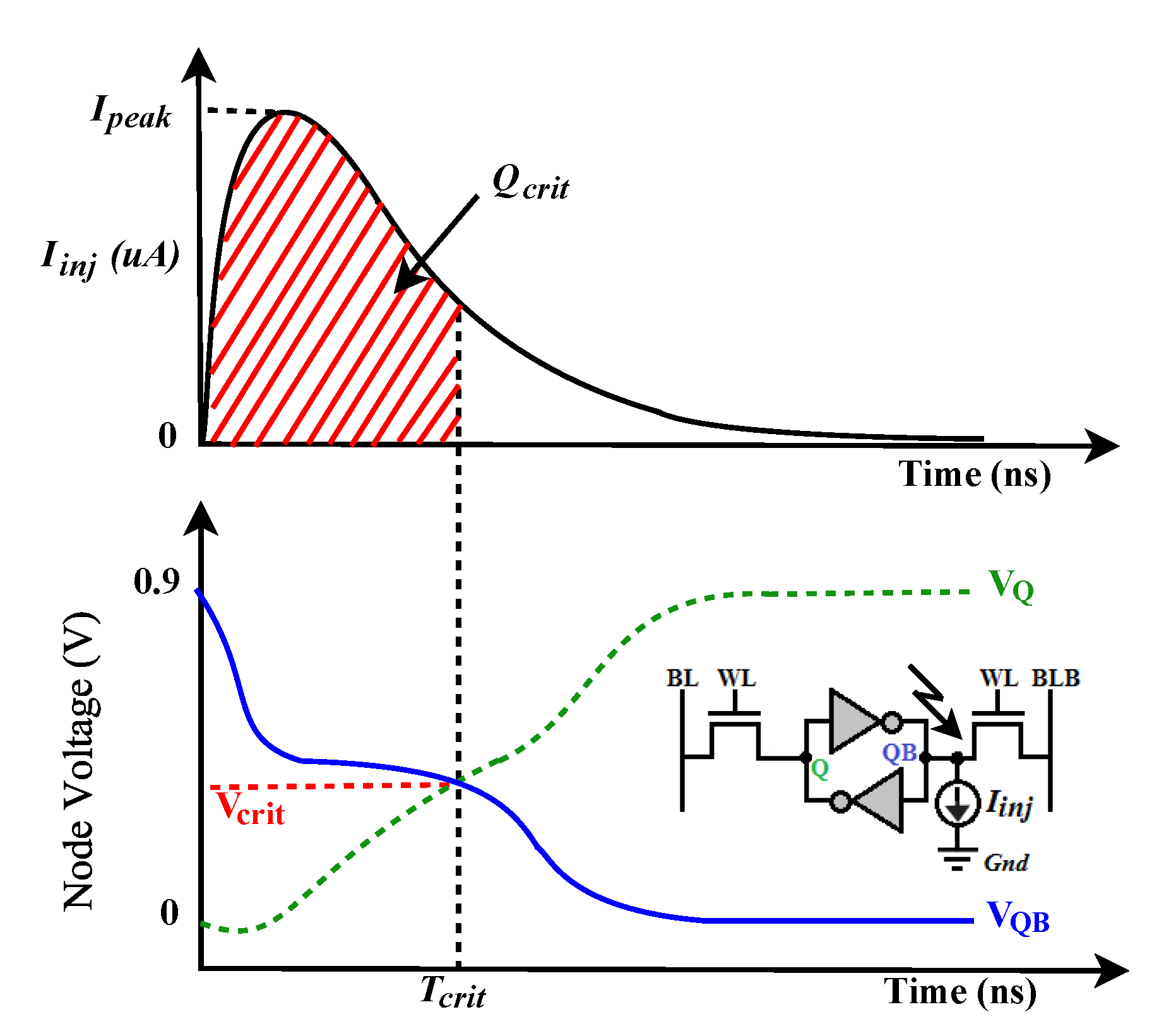
Q inj is the total amount of charge deposited at the sensitive node, and I peak is the peak value of the equivalent current source. TThe characteristic time constants τ f and τ r are material dependent parameters. As suggested in [5], we have used typical values of τ f = 1 ps and τ r = 50 ps. In our simulations the critical charge Q crit is determined by injecting the current peak at the sensitive node of the respective SRAM cell, as shown in Figure 5, which simulates a possible particle strike.
To estimate the critical charge at the storage nodes of the discussed SRAM cells we assumed that either ‘0’ and ‘1’ is stored at storing nodes Q and Q B , respectively. Since the carrier mobility of the NMOS transistor is higher than for the PMOS transistor, the node storing ‘1’ is more susceptible to any soft errors than node storing ‘0’ [12]. Therefore, we consider the node Q B as the weakest node being responsible for the effective critical charge Q crit of the SRAM cells. Figure 6 shows the critical charge at the nodes Q and Q B for the considered SRAM cells. It can be observed that the critical charge at node Q is higher than the critical charge at node Q B , and the proposed AS10T cell exhibits the highest critical charge amongst all studied cells, i.e., the critical charge of the AS10T is 75.83%, 75.41%, and 0.14% higher compared to the 6T, RD8T, and AS8T SRAM cell. The AS10T and AS8T has the higher critical charge because the charge booster is connected between the storage nodes. The charge booster increases the current path at the sensitive nodes which increases the node capacitance and hence increases the soft error tolerance. The AS10T behaves similar to AS8T in terms of the critical charges of the most sensitive nodes. Based on the above observation Q B is considered the most sensitive node of the SRAM cells for further analysis.

Effect of Supply Voltage Variation and Temperature Variation on the Critical Charge

Next, the critical charge is calculated for different supply voltages and device temperatures for 6T and AS10T SRAM cell, as shown in Figure 7. It can be observed that the critical charge for the AS10T cell is higher at each supply voltage and temperature. It has to be noted that the higher the critical charge is the better the hardening with respect to soft errors is. Thus, the proposed AS10T cell exhibits enhanced soft error hardening compared to the 6T SRAM cell, and also compared to the other cells. As can be further seen, the critical charge reduces with increasing temperature, whereas the critical charge increases at larger supply voltages. From the above discussions, the critical charge change with temperature and supply voltage can be modeled as:
Q crit + Δ Q crit = k × ( V dd + Δ V dd ) n × ( T + Δ T ) ,
where k and n are technology and material-dependent constants. The parameter k depends linearly on the supply voltage, whereas n depends exponentially on the operating temperature. Δ Q crit is the change in critical charge due to a change in supply voltage ( Δ V dd ) and operating temperature ( Δ T ). Further, we also analyze the effect of SEU with different t r and t f on the sensitive node of the 6T and AS10T cell, as shown in Figure 8. Our results demonstrate that the critical charge mainly depends on the t f because it determines the total charge stored at the sensitive node of the SRAM cells, as depicted in Figure 5. When the fall time t f of the injected pulse increases the charge collection probability also increases, which provides a higher critical charge at the sensitive nodes of the SRAM cells.

3.3. Aging Effects on Performance of SRAM Cells

As mentioned before, the performance integrated MOS transistors can change over time [13]. In general, BTI are considered responsible for the aging of the devices. In the following we analyze the stability of the SRAM cells and the evolution of the critical charge when BTI is being considered as consequence of device stress.

3.3.1. Effects on SRAM Stability

For the analysis of aging effects on the HSNM of the 6T and AS10T SRAM cell, we consider NBTI and PBTI during stress for PMOS and NMOS transistors, respectively. The DC stress is calculated to be applied for three years of stress time. The effect of BTI on the 6T and AS10T SRAM stability for hold operation is given in Table 2. The result shows that the HSNM reduces by 2.13% and 1.92% for the 6T and AS10T cell, respectively, considering only NBTI, and 4.26% and 3.85% for 6T and AS10T cell respectively, when considering both NBTI and PBTI. Results demonstrate that the AS10T is slightly less affected by BTI compared to the 6T SRAM cell, which indicates that the AS10T cell is more stable in terms of BTI.

3.3.2. Effects on Critical Charge

To analyze the effect of BTI on soft error susceptibility, we calculated the critical charge while considering the impact of BTI for a stress time of three years. Table 3 shows the critical charge variation observed at the sensitive node of the 6T and AS10T SRAM cell with stress considering NBTI and PBTI. The result shows that the critical charge decreases with stress time. The critical charge of the 6T and AS10T is reduced by 6.39% and 0.84%, respectively, when considering only NBTI. Similarly, the critical charge of the 6T and AS10T is reduced by 7.86% and 0.98%, respectively, when again considering only NBTI. This indicates that the critical charge of AS10T is slightly less affected by the BTI as compared to the 6T SRAM cell and thus the proposed cell is more robust against aging effects.

3.4. Process, Voltage and Temperature Variation Analysis

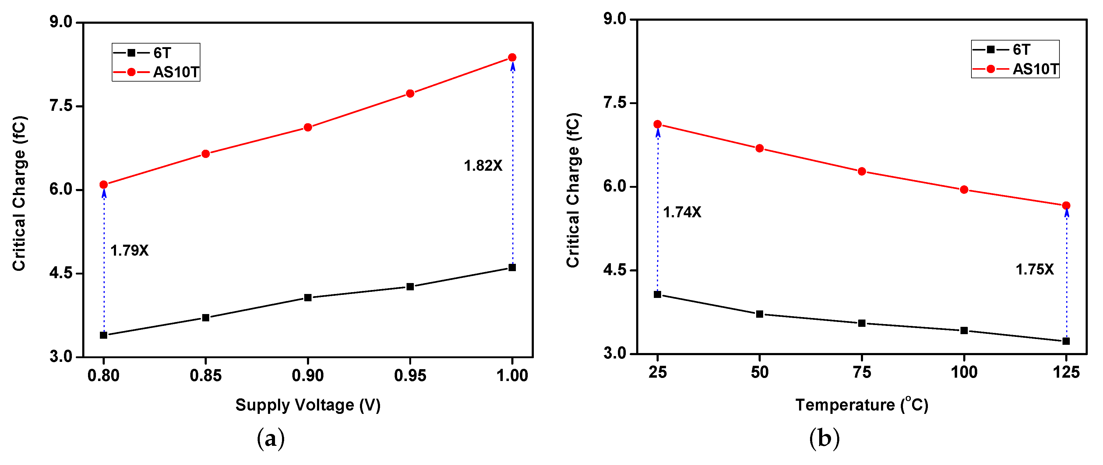
The impact of process, voltage and temperature (PVT) variations on the soft error tolerance is an important measure for the stable operation of the circuit. The effect of supply voltage and temperature variations on the critical charge of sensitive node Q B is shown in Figure 9. Figure 9a shows the evolution of the critical charge with supply voltage variation in the range of V dd = 0.8 V to 1 V for the considered circuits. The results reveal that the critical charge increases with the supply voltage as the node capacitance increases with the same. It is also observed that the critical charge for proposed AS10T is higher compared to the 6T SRAM cell indicating that the proposed AS10T cell is more hardened to soft errors caused by supply variations. Figure 9b shows the trend of the critical charge with the temperature ranging from T = 25 °C to T = 125 °C. The results show that with the increasing temperature, the critical charge decreases because the device carrier mobility decreases.
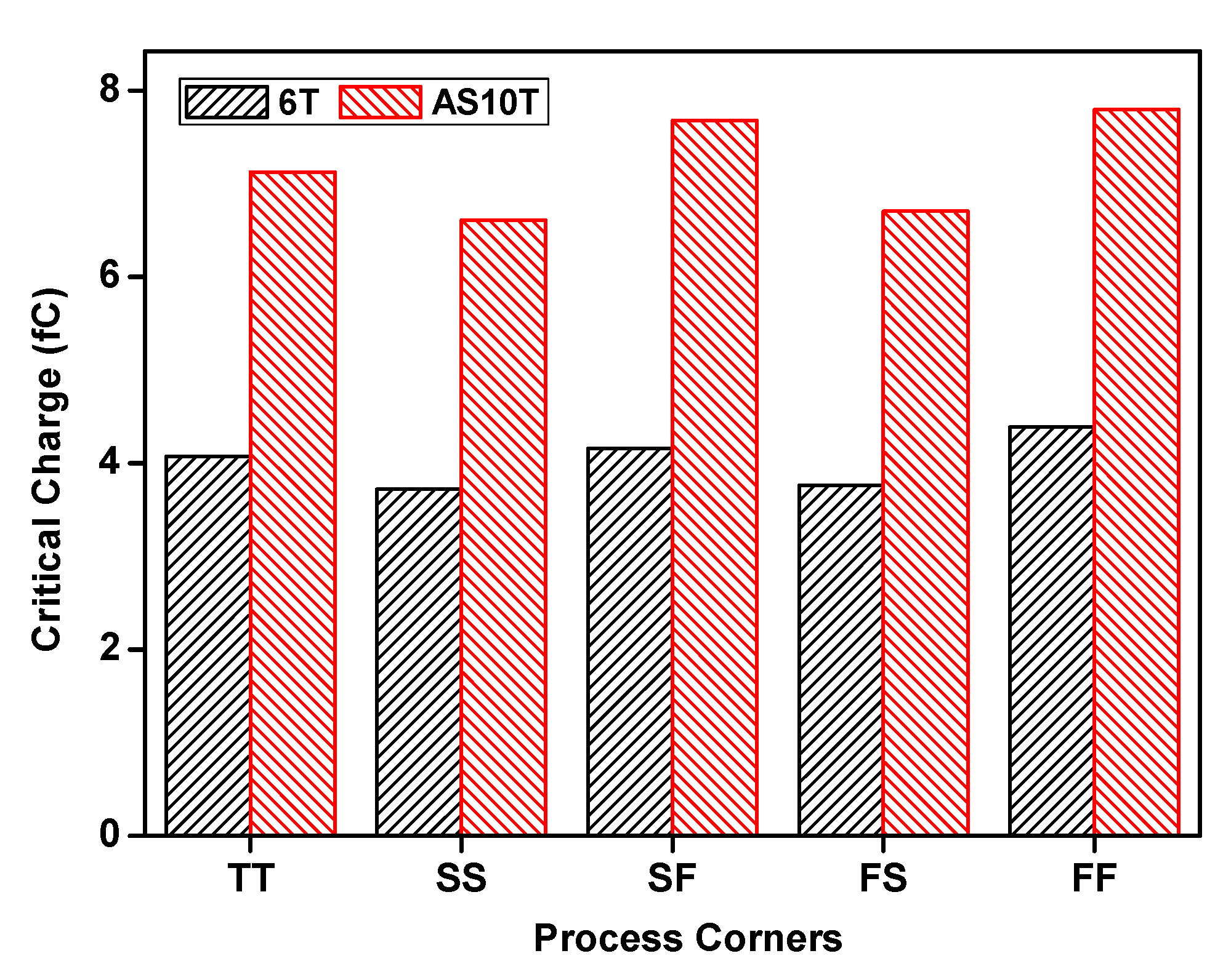
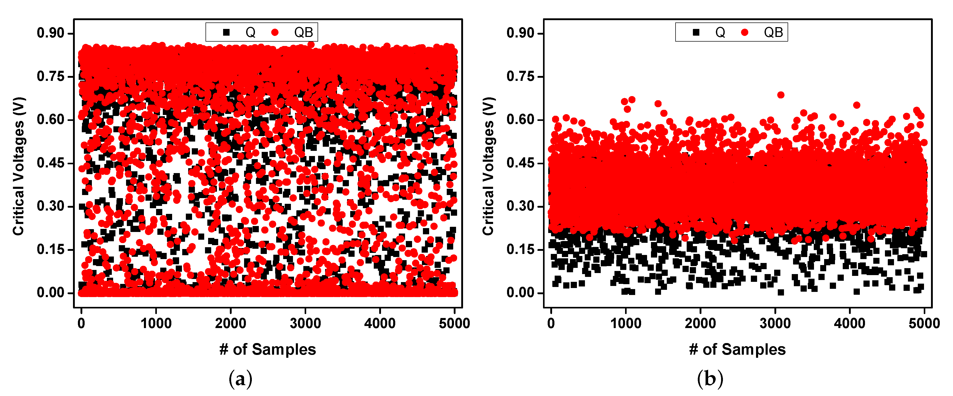
Further, we analyzed the critical charge for the 6T and AS10T cell for the process corners [Fast-Fast (FF), Fast-Slow (FS), Slow-Fast (SF), Slow-Slow (SS), and Typical-Typical (TT)], as shown in Figure 10. The results show that the critical charge for the AS10T is higher than that of the 6T cell for all the process corners. Additionally, for the analysis of soft error resilience and process variations on the 6T and AS10T SRAM cells, we perform 5000 Monte Carlo simulations for the critical voltages of the storage node considering the variations in the threshold voltage of the transistors as depicted in Figure 11. The simulation result shows that the AS10T SRAM cell has less effect of process variations as compared to 6T SRAM cell. Results demonstrate that the significant portion of critical voltage repeatability for the 6T cell is near 0V, which indicates that the flipping of logic in these SRAM cells can be triggered earlier as compared to AS10T SRAM cell.

3.5. Power Consumption Analysis

The power consumption during hold operation with supply and temperature variation for 6T and AS10T SRAM cell is shown in Figure 12. For our analysis we considered the supply voltage ranging from V dd = 0.8 V to 1 V and the operating temperature ranging from T = 25 °C to T = 125 °C. The power dissipation increases with increasing supply voltage and increasing temperature. The results show that the AS10T cell has less power variation with supply voltage and temperature as compared to the 6T SRAM cell.

4. Conclusions

This paper presents a radiation-hardened asymmetric a 10T (AS10T) SRAM cell to enhance the soft error hardening, considering aging effects like bias temperature instabilities. The proposed cell uses a read decoupled path to improve read static noise margin and a voltage booster connected between the storage nodes to improve node capacitance, and finally lead to an enhanced radiation hardening. We demonstrated that the AS10T SRAM cell has a higher critical charge at the most sensitive node compared to other SRAM cells. Further, we analyze the effect of BTI on soft error susceptibility on the critical charge and on the stability of the SRAM cells and observe that the AS10T cell is more resilient to aging effects. Therefore, we conclude that the proposed SRAM cell can be used for applications, which demand not only high speed but especially also a radiation-hardened design and high operating stability with considerable chip area.

Author Contributions

Conceptualization, A.P.S.; methodology, A.P.S.; software, A.P.S.; validation, A.P.S.; formal analysis, A.P.S.; investigation, A.P.S.; resources, A.P.S.; data curation, A.P.S.; writing—original draft preparation, A.P.S.; writing—review and editing, M.W.; visualization, M.W.; supervision, M.W.; project administration, M.W.; funding acquisition, M.W. All authors have read and agreed to the published version of the manuscript.

Funding

The research leading to this work has received substantial funding from the Take-off program of the Austrian Research Promotion Agency FFG (projects no. 861022 and 867414).

Conflicts of Interest

The authors declare no conflict of interest.

References

  1. Ferlet-Cavrois, V.; Massengill, L.W.; Gouker, P. Single event transients in digital CMOS—A review. IEEE Trans. Nucl. Sci. 2013, 60, 1767–1790. [Google Scholar] [CrossRef]
  2. Heidel, D.F.; Rodbell, K.P.; Oldiges, P.; Gordon, M.S.; Tang, H.H.K.; Cannon, E.H.; Plettner, C. Single-event-upset critical charge measurements and modeling of 65 nm silicon-on-insulator latches and memory cells. IEEE Trans. Nucl. Sci. 2006, 53, 3512–3517. [Google Scholar] [CrossRef]
  3. Rossi, D.; Omaña, M.; Metra, C.; Paccagnella, A. Impact of bias temperature instability on soft error susceptibility. IEEE Trans. Very Large Scale Integr. (VLSI) Syst. 2015, 23, 743–751. [Google Scholar] [CrossRef] [Green Version]
  4. Chang, L.; Fried, D.M.; Hergenrother, J.; Sleight, J.W.; Dennard, R.H.; Montoye, R.K.; Sekaric, L.; McNab, S.J.; Topol, A.W.; Adams, C.D.; et al. Stable SRAM cell design for the 32 nm node and beyond. In Digest of Technical Papers Symposium on VLSI Technology; IEEE: Kyoto, Japan, 2005; pp. 128–129. [Google Scholar]
  5. Alouani, I.; Elsharkasy, W.M.; Eltawil, A.M.; Kurdahi, F.J.; Niar, S. AS8-static random access memory (SRAM): Asymmetric SRAM architecture for soft error hardening enhancement. IET Circuits Devices Syst. 2017, 11, 89–94. [Google Scholar] [CrossRef]
  6. Ahmad, S.; Alam, N.; Hasan, M. Pseudo differential multi-cell upset immune robust SRAM cell for ultra-low power applications. AEU-Int. J. Electron. Commun. 2018, 83, 366–375. [Google Scholar] [CrossRef]
  7. Kim, J.S.; Chang, I.J. We-quatro: Radiation-hardened SRAM cell with parametric process variation tolerance. IEEE Trans. Nucl. Sci. 2017, 64, 2489–2496. [Google Scholar]
  8. Sanvale, P.; Gupta, N.; Neema, V.; Shah, A.P.; Vishvakarma, S.K. An improved read-assist energy efficient single ended PPN based 10T SRAM cell for wireless sensor network. Microelectron. J. 2019, 92, 104611. [Google Scholar] [CrossRef]
  9. Predictive Technology Model (PTM). Available online: http://ptm.asu.edu/ (accessed on 12 December 2017).
  10. Synopsys. HSPICE User Guide: Simulation and Analysis 2010. Available online: https://www.ele.uri.edu/Courses/ele448/HspiceRef/hspice_sa.pdf (accessed on 2 December 2019).
  11. Jahinuzzaman, S.M.; Sharifkhani, M.; Sachdev, M. An analytical model for soft error critical charge of nanometric SRAMs. IEEE Trans. Very Large Scale Integr. (VLSI) Syst. 2009, 17, 1187–1195. [Google Scholar] [CrossRef]
  12. Lin, S.; Kim, Y.B.; Lombardi, F. Design and analysis of a 32 nm PVT tolerant CMOS SRAM cell for low leakage and high stability. Integr. VLSI J. 2010, 43, 176–187. [Google Scholar] [CrossRef]
  13. Shah, A.P.; Yadav, N.; Beohar, A.; Vishvakarma, S.K. On-chip Adaptive Body Bias for Reducing the Impact of NBTI on 6T SRAM Cells. IEEE Trans. Semicond. Manuf. 2018, 31, 242–249. [Google Scholar] [CrossRef]
Figure 1. Threshold voltage degradation (in percent of initial threshold voltage) for the PMOS/negative bias temperature instabilities (NBTI) and NMOS/ positive bias temperature instabilities (PBTI) case as predicted by the HSPICE for a 32 nm technology node considering DC stress. The rate of threshold voltage degradation is high for the initial years and tends to saturate over time.
Electronics 09 00256 g001
Figure 2. Schematic of different SRAM Cells: (a) 6T SRAM cell (b) Read decoupled 8T (RD8T) SRAM cell after (c) Asymmetric radiation-hardened 8T (AS8T) SRAM cell after (d) Proposed asymmetric radiation-hardened (AS10T) SRAM Cell with improved stability.
Electronics 09 00256 g002
Figure 3. (a) Write margin (WM), hold static noise margin (HSNM), and read static noise margin (RSNM) of different SRAM cells; (b) Butterfly curve for read operation and RSNM of the 6T and AS10T SRAM cells. The margins are calculated considering a supply voltage of V dd = 0.9 V and T = 25 °C.
Electronics 09 00256 g003
Figure 4. Simulation flow of soft-error analysis with embedded aging effects.
Electronics 09 00256 g004
Figure 5. Graphical representation defining the critical charge. (top) Shows the transient behavior of the current pulse representing a possible particle strike. (bottom) V Q and V QB are the storage node voltages of the SRAM cell. Simulation setup for an high energy particle hitting a sensitive node V Q B storing ‘1’ of a SRAM cell is given in the inset.
Electronics 09 00256 g005
Figure 6. Critical charge at the storage nodes of SRAM cells considering logic ‘0’ and ‘1’ are stored at nodes Q and Q B , respectively.
Electronics 09 00256 g006
Figure 7. Critical charge variation at different supply voltages and temperatures for the (a) 6T SRAM cell and the (b) AS10T SRAM cell.
Electronics 09 00256 g007
Figure 8. SEU effect on the observed critical charge of sensitive nodes of the SRAM cells simulated considering different rise times ( t r ) and fall times ( t f ) of the injected double exponential current pulse at the sensitive nodes.
Electronics 09 00256 g008
Figure 9. Critical charge at the sensitive node of SRAM cells (a) with supply voltage variation (b) with temperature variation.
Electronics 09 00256 g009
Figure 10. Critical charge at the sensitive node of SRAM cells for different process corners.
Electronics 09 00256 g010
Figure 11. Distribution of critical voltages ( V crit ) with 5000 Monte Carlo samples for V Q and V QB for (a) 6T SRAM cell (b) AS10T SRAM cell. The distribution indicates the repeatibility of the critical voltage for 6T and AS10T SRAM cells.
Electronics 09 00256 g011
Figure 12. Power consumption for supply voltage and temperature variation for the (a) 6T SRAM cell and the (b) AS10T SRAM cell.
Electronics 09 00256 g012
Table 1. Control signals of proposed AS10T SRAM cell for different operations. Write ‘0’ and Write ‘1’ correspond to the storage node Q. BL and BLB are the bit-lines and are complementary to each other. RBL is bit-line during read operation. WWL and RWL are the word-lines during write and read operations, respectively.
OperationsControl Signals
BLBLBWWLRWLRBL
Write 001100
Write 110100
Hold××000
Read1×111
Table 2. HSNM of different SRAM cells with and without BTI after the stress time of three years.
Stress6TAS10T
No stress332.3 mV367.6 mV
NBTI325.2 mV360.6 mV
NBTI + PBTI318.2 mV353.5 mV
Table 3. Critical charge (fC) at the sensitive node of the respective SRAM cells with and without BTI after three year of stress time. For BTI both, NBTI/PMOS and PBTI/NMOS occurring in transistors, are considered.
Stress Time6TAS10T
(Years)NBTIBTINBTIBTI
04.074.077.127.12
13.883.837.087.07
23.843.787.077.06
33.813.757.067.05