Article

Dual-/Tri-Wideband Bandpass Filter with High Selectivity and Adjustable Passband for 5G Mid-Band Mobile Communications

1
Hubei Engineering Research Center of RF-Microwave Technology and Application, Wuhan University of Technology, Wuhan 430070, China
2
School of Science, Wuhan University of Technology, Wuhan 430070, China
3
School of Information Engineering, Wuhan University of Technology, Wuhan 430070, China
*
Authors to whom correspondence should be addressed.
Electronics 2020, 9(2), 205; https://doi.org/10.3390/electronics9020205
Submission received: 20 December 2019 / Revised: 16 January 2020 / Accepted: 20 January 2020 / Published: 22 January 2020
(This article belongs to the Section Microwave and Wireless Communications)

Abstract

:
The design and implementation of the filters for the fifth-generation (5G) mobile communication systems are challengeable due to the demands of high integration, low-cost, and high-speed data transmission. In this paper, a dual-wideband bandpass filter (BPF) and a tri-wideband BPF for 5G mobile communications are proposed. The dual-wideband BPF consists of two folded open-loop stepped-impedance resonators (FOLSIRs), and the tri-wideband BPF is designed by placing a pair of folded uniform impedance resonator inside the dual-wideband BPF with little increase in the physical size of the filter. By employing a novel structural deformation of a stepped-impedance resonator, the FOLSIR is achieved with a more compact structure, a controllable transmission zero, and an adjustable resonant frequency. The measurement results show that the working bands of the two filters are 1.98–2.28/3.27–3.66 GHz and 2.035–2.305/3.31–3.71/4.54–5.18 GHz, respectively, which are consistent with the full-wave EM simulation results. The implemented filters have a compact size and the results show low loss, good out-of-band rejection, and wide passbands covering sub-6 GHz bands of 5G mobile communications and a commonly used spectrum.

1. Introduction

In 2015, the International Telecommunication Union-Radio Communication Sector (ITU-R, Geneva, Switzerland) defined three typical usage scenarios for the fifth-generation mobile communication system (5G), including enhanced mobile broadband (eMBB), massive machine-type communications (mTC), and ultrareliable and low-latency communication (uRLLC) [1]. High-integration, low-cost, and high-speed data transmission are required for these application scenarios of 5G mobile communication systems. As a key component of wireless communication systems, multi-band bandpass filters (BPFs) with compact size, low loss, and wide passbands are envisioned as potential techniques to meet the requirements brought by 5G mobile communications [2,3,4].
Currently, four methods have been employed in the construction of multi-band BPFs. Multi-mode resonator is one of the basic theories for multi-band BPFs. By combining two or more resonant modes of a multi-mode resonator, for instance, ring multi-mode resonators [5,6,7,8] and multi-mode stub-loaded resonators (SLRs) [9,10,11], the passband of the filter is formed. Combining more modes in one passband will increase the bandwidth [12]. In Ref [10], a compact tri-band BPF is developed by multi-mode SLR, but with small bandwidth and large insertion loss. In addition, by utilizing the coupling between two multi-mode resonators, the odd–odd and even–even resonant modes contribute to the passbands, such as stepped-impedance resonators (SIRs) in tri-band BPFs [13] and dual-band BPFs [14,15], SLRs in tri-band BPFs [16,17], and dual-band BPFs [18,19,20]. In Ref [14], a compact dual-band bandpass filter is obtained by coupling between two modified SIRs; the bandwidth can be adjusted using coupling strengths between resonators, but with large insertion losses and narrow passbands. The third method is to add structures with stopbands or transmission zeros (TZs) in BPFs [21,22] or lowpass filters [23], and to divide one passband into more passbands. Due to the added structures, the resulting multi-band BPFs often have large size [21,22] or complex structures [23]. Feeding parallel filter cells through common input/output (I/O) ports is the fourth way, with the advantage of designing and adjusting each passband independently [24,25,26,27]. However, due to the stacking of the parallel filter cells, the resulting multi-band BPFs usually have larger size [25,26,27]. Using resonators of a filter cell as I/O ports for the other filter cells is an improvement of this method. Due to the embedded structure, the resulting multi-band BPFs usually have compact size [28,29] and adjustable passbands [30,31].
In recent years, several new technologies have also been used in the design of multi-band BPFs. In Ref [32], the multi-mode characteristic of substrate-integrated waveguide (SIW) is employed for a 5G dual-band BPF, but the size is relatively large. In Ref [33], a dual-band transparent a graphene microstrip filter for 5G is designed; nevertheless, large insertion loss limited the application of this filter. To our best knowledge, the tri-band BPFs for 5G mobile communication systems with compact size, low loss, and wide passbands have not been proposed and discussed in the literatures.
In this paper, a dual-wideband BPF and a tri-wideband BPF for 5G mobile communications are proposed. The dual-wideband BPF is achieved by two folded open-loop stepped-impedance resonators (FOLSIRs), and then by placing a pair of folded uniform impedance resonators (FUIRs) inside the dual-wideband BPF, a tri-wideband BPF is constituted with little influence in the physical size of the filter. Most importantly, the FOLSIR in our filters is obtained by a novel structural deformation of SIR. In the existing multi-band BPFs researches, the center frequencies (CFs) of passbands are usually reduced by increasing the length or width of loaded stubs [34,35,36,37]. However, the increase of the CFs is limited when the loaded-stub length is reduced to zero. In our design, by changing width of the folded portion of the FOLSIR, the CF of the second passband can be freely increased or decreased. Cross-coupling of the resonators generates more TZs to improve the band-to-band isolation and out-of-band rejection level. The two multi-wideband BPFs are simulated by a commercial full-wave electromagnetic (EM) simulator Ansys HFSS and fabricated on a Rogers 5880 substrate with a relative permittivity εr of 2.2 and thickness of 0.787 mm. Measurements are conducted with a network analyzer, the implemented filters have a compact size, and the results show low loss, good out-of-band rejection, and wide passbands covering sub-6 GHz bands and other commonly used spectrum. The design principle and simulated results are well verified by measurement of the fabricated filters, and good consistency between simulation and measurement are obtained.
This paper is arranged as follows. In Section 2, the FOLSIR and FUIR are analyzed based on theory and electromagnetic simulation, and an equivalent circuit diagram of the FOLSIR is proposed to explain the principle of resonant frequency and TZ adjustment. In Section 3, the dual-wideband BPF and the tri-wideband BPF with coupled FOLSIR and FUIR are designed, simulated, characterized, and optimized. In Section 4, the measurement results of a manufactured dual-wideband BPF and tri-wideband BPF are presented and discussed, which verifies the proposed method. Conclusions are drawn in Section 5.

2. Resonator Analysis

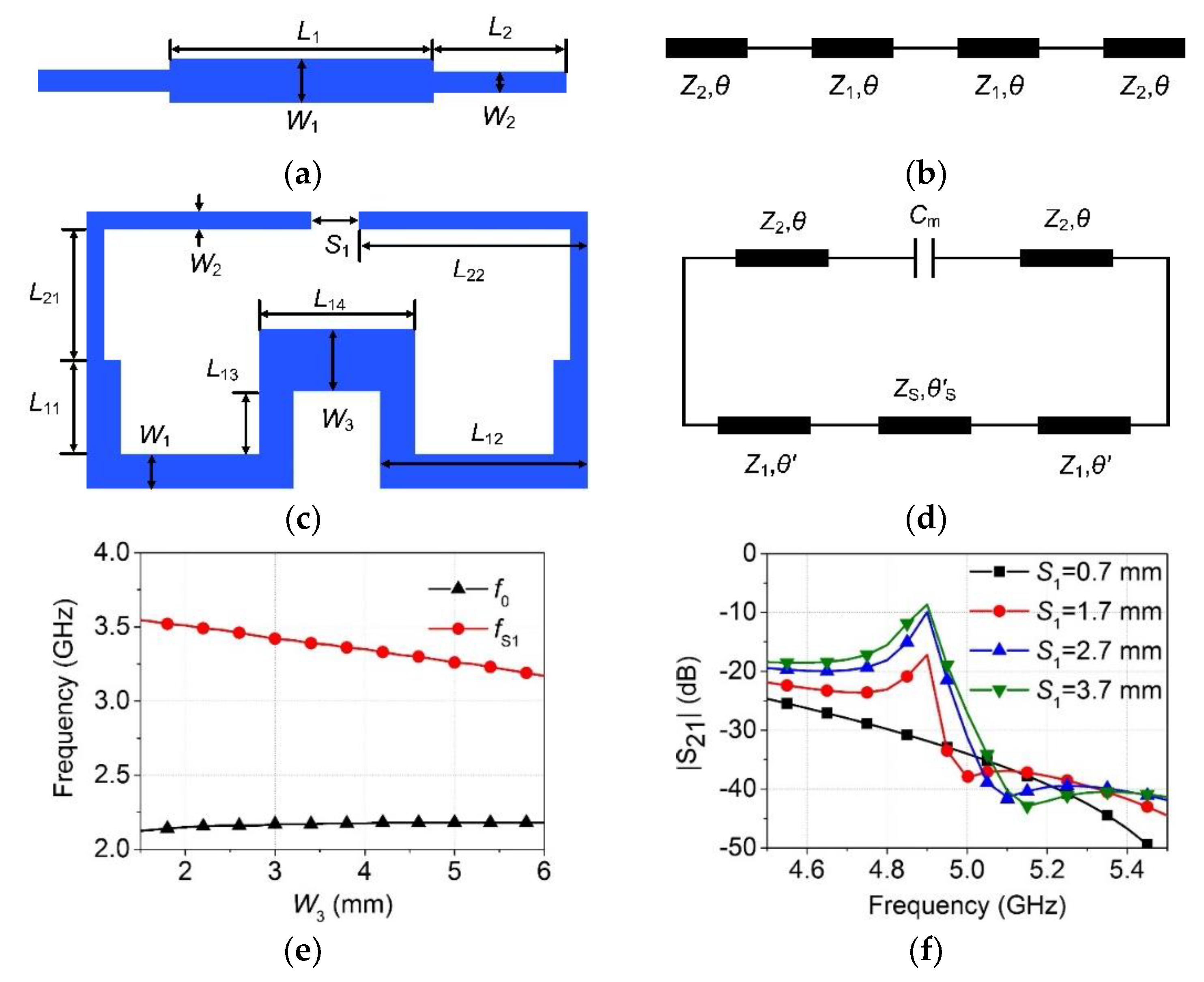
2.1. FOLSIR Analysis
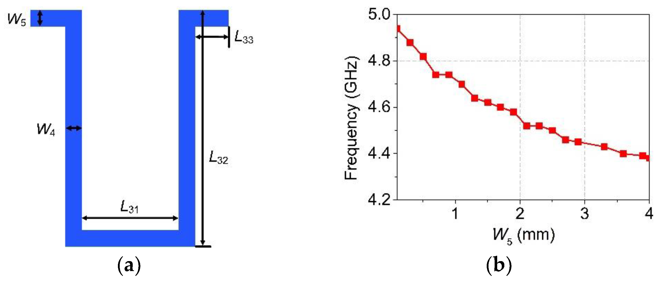
SIR has been widely used in the design of multi-band BPFs. SIR consists of parts with different characteristic impedance. As shown in Figure 1a, a λg/2 SIR is composed of a low-impedance part (LIP) in the center and two high-impedance parts (HIPs) at both sides, the length of the LIP is λg/4, and the length of the two HIPs are all λg/8. In order to explain the principle of the resonators more clearly, an equivalent circuit diagram of the SIR is presented, as shown in Figure 1b. It can be seen from Figure 1b that the characteristic impedances of the LIP and HIP of the SIR are Z1 and Z2, the LIP in the center has an electrical length of 2θ, and the electrical length of the HIP on each side is θ. The relationship between the resonant frequencies and characteristic impedance ratio, the electrical length of the SIR, is described as [38]:
θ = arctan R Z ,
f S 1 f 0 = π 2 arctan R Z ,
where f0 is the resonant frequency of the SIR, fS1 is the first spurious resonant frequency of the SIR, θ is the electrical length of each part, and RZ = Z2/Z1 is the characteristic impedance ratio of HIP and LIP. With the microstrip as the fundamental structure, the characteristic impedance of each part is determined by the formulas such as following:
Z 0 = 120 π ε re 1 W / h + 1.393 + 0.667 ln ( W / h + 1.444 ) ,
ε re = ε r + 1 2 + ε r 1 2 ( 1 + 12 h W ) 1 2 ,
when W/h >1, and the substrate used in this paper meets this requirement, where W is width of the conductor, h is the thickness of the grounded dielectric substrate, and εr is the dielectric constant of the substrate.
According to Equations (1)–(4), the physical size of the SIR can be calculated if f0 and fS1 are given. In order to reduce the size and increase a transmission zero, the SIR is bent directly on the physical structure to form a FOLSIR, as shown in Figure 1c. The LIPs and HIPs of the FOLSIR still have the same widths of W1 and W2 as the SIR, the length of the HIP is L21 + L22 = L2, and the length of the LIP is L11 + L12 + L13. Particularly, a serial step impedance part with a width of variable W3 is added between the two LIPs, which has a length of L14 and 2(L11 + L12 + L13) + L14 − 2W1 = L1. The serial step impedance part with a width of variable W3 is used to neutralize the variation in the transmission line characteristics caused by the structural change from SIR to FOLSIR. This ensures that FOLSIR has the expected resonant frequencies f0 and fS1.
Compared to SIR, the equivalent circuit diagram of FOLSIR in Figure 1d adds a coupling capacitor Cm and a section with characteristic impedance ZS corresponding to variable W3. The electrical length of the serial step impedance part with characteristic impedance ZS is θ S and the separated LIPs are shortened to θ’, and 2θ’ + θ S = 2θ.
Since there are four parts that make up the λg/2 SIR, the length of each part is λg/8. So, the input impedance formula of each part can be rewritten from Equation (5) to Equation (6).
| Z in ( l ) | = | Z 0 Z L + j Z 0 tan β l Z 0 + j Z L tan β l | ,
| Z in | = | Z 0 Z L + j Z 0 Z 0 + j Z L | ,
where Z0 is the characteristic impedance, ZL is the load impedance, and βl = θ, the same as Equation (7).
For the SIR, when calculating the input impedance of the HIP, looking from the LIP to the HIP, Z0 = Z2. Since the terminal is open, the load impedance is ZL = ∞, substituting Z0 = Z2 and ZL = ∞ into Equation (5), then the input impedance is Zin2 = -jZ2. The input impedance at the center of the LIP is determined by substituting Zin2 into Equation (6).
For the FOLSIR, when calculating the input impedance of the HIP, looking from the LIP to the HIP, Z0 = Z2, and for the terminal is coupling capacitor Cm, which is determined by the gap S1 of the two HIPs, the load impedance is ZL = 1/(jωCm). Using the same procedure as for the SIR in the above paragraph, it can be found that the input impedance at the connection of the HIP with LIP and the center of the LIP are different from that of the SIR. According to Equation (2), the aimed f0 and fS1 cannot be satisfied because of the different input impedances.
So, the influence of Cm on the resonant frequencies of FOLSIR must be eliminated by impedance transformation; this is realized using the added serial step impedance part. In this paper, the gap between the width W1 of the HIP and W3 of the added part is determined in the optimum procedure by a full-wave EM simulator.
To satisfy the diversified industrial demand, passbands of filters should be adjustable during the design phase [33]. Therefore, a novel passband adjustment method is proposed in this paper. Take the values f0 = 2.14 GHz and fS1 = 3.5 GHz, and the initial physical size of FOLSIR is calculated by Equations (1)–(4), in which W1 = W3 = 2.425 mm and W2 = 0.672 mm. By decreasing or increasing W3 from W3 = 2.425 mm, fS1 can be increased or decreased, respectively, while f0 shows little change, as shown in Figure 1e. The reason for this phenomenon is that the rise of W3 caused a drop of ZS, and then the characteristic impedance of the LIP is decreased, which means an increasing in the characteristic impedance ratio of the FOLSIR. According to Equations (1) and (2), the value of fS1/f0 would witness a decline. These have been proven in the previous analysis of the FOLSIR.
In Figure 1f, we can see a TZ, which is generated by the coupling of FOLSIR. In the equivalent circuit, the end of the open loop transmission line is connected by a lumped capacitor Cm, which is called an electrical coupling path [39]. By changing the lumped capacitor Cm, the coupling value of the coupled paths will affect the TZ. A simulation experiment verification is shown in Figure 1f; the TZ decreases as S1 decreases. When S1 = 0.7 mm, the second spurious resonant frequency of FOLSIR is completely suppressed. After the above analysis, the FOLSIR can be used to design a dual-band BPF with an adjustable passband and a wide rejection band.

2.2. FUIR Analysis

In order to adapt to the limited space, the FUIR is proposed and it inherited the calculation theory of the uniform impedance resonator (UIR), as shown in Figure 2a. After determining the microstrip substrate parameters, the relationship between electrical length θ, width W, and resonant frequency f0 of the FUIR can be expressed as follows [40]:
θ = β l ,
β = 2 π λ g ,
λ g = λ 0 ε r e = c f 0 ε r e .
The quarter-wavelength FUIR is selected, and the physical size of the resonator can be calculated based on the desired f0. In order to place the FUIRs inside the dual-wideband BPF and fed by FOLSIRs to generate the required resonant frequency, the FUIR is folded into a suitable structure, and the total length of the FUIR L (L = L31 + 2 × (L32 + L33)) is reduced, while the width W (W = W4 = W5) is increased.
According to the calculation theory of the FUIR above, f0 can be adjusted by changing L or W, and when one of either W or L is constant, the increase of the other one causes a decrease of f0. The prediction results according to the theoretical Equation (4) and Equations (7)–(9) are verified by the simulation results of W5 ranging from 0.1 to 4 mm, while L = 24.54 mm, as shown in Figure 2b.

3. Filter Design

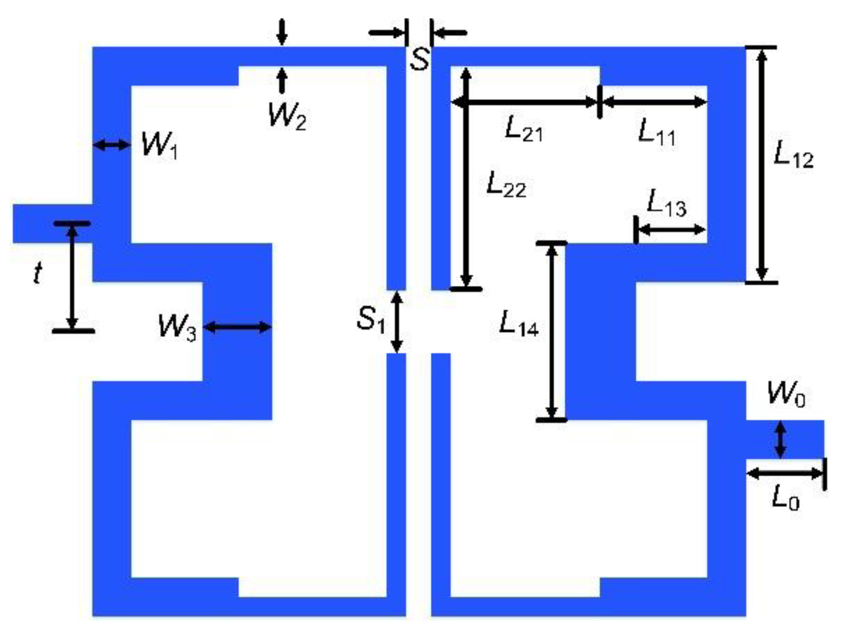
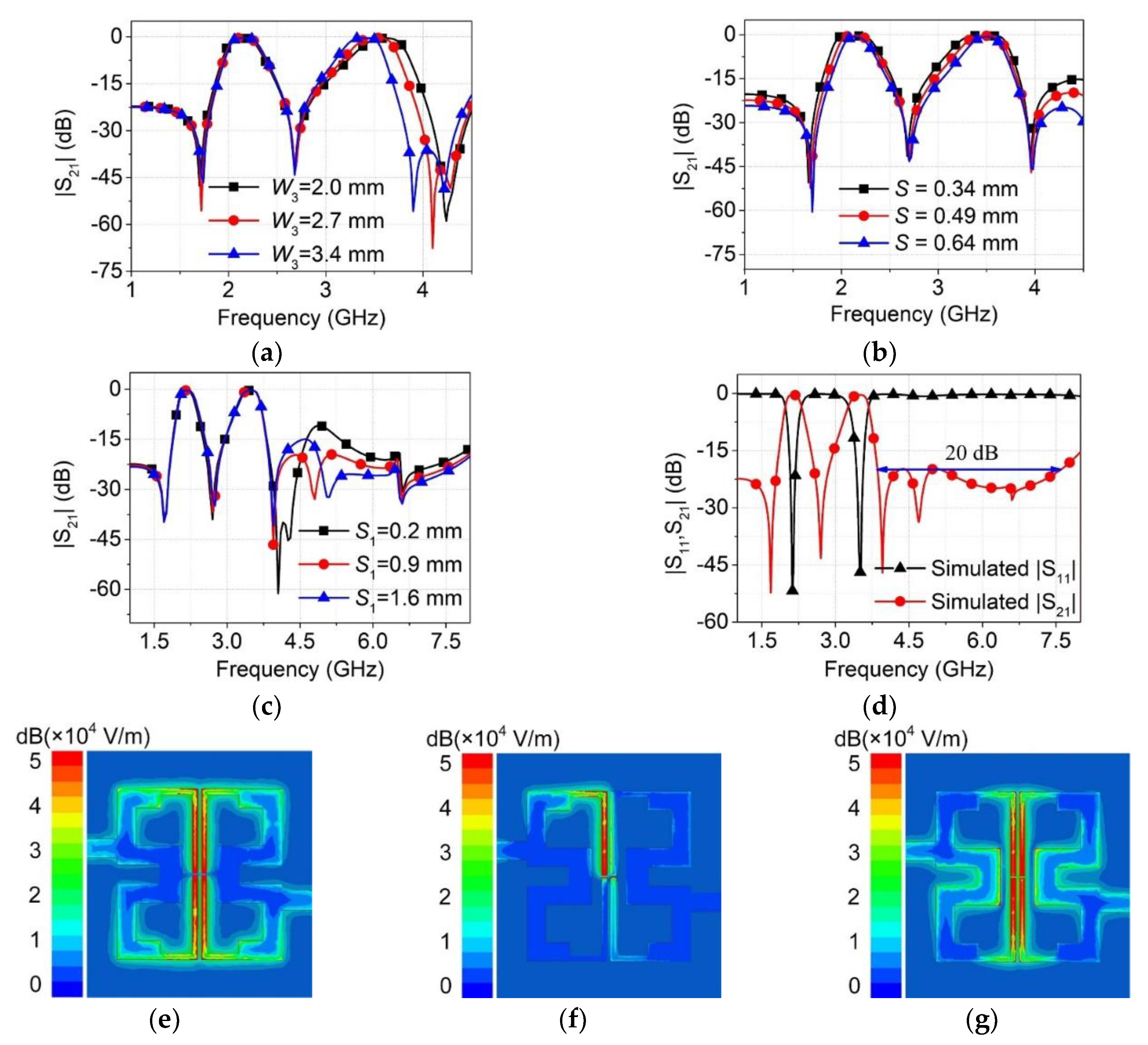
3.1. Dual-Wideband BPF Design

According to the theory analysis in the previous section, we set f0 and fS1 to 2.14 GHz and 3.5 GHz, respectively, and the physical size of the FOLSIR is obtained after calculation, in which W1 = W3 = 2.425 mm and W2 = 0.672 mm. The schematic diagram of the proposed dual-wideband BPF is shown in Figure 3, which is composed of two FOLSIRs. Two 50-Ohm feed lines are directly tapped onto the resonators, and the coupling or the external quality factor is controlled by the tapping position t. The decrease of the t results in a weaker coupling or a larger external quality factor [40].
A commercial full-wave EM simulator is used to model and simulate the dual-wideband BPF. It is found that the theoretical calculation has deviation from the simulation results, and the simulation results need to be optimized. In some previous studies, an open loaded stub and short loaded stub are used to adjust the CFs of passbands, and the CFs of passbands are usually reduced by increasing the length or width of loaded stubs [34,35,36,37]. However, the increase of the CFs is limited when the loaded-stub length is reduced to zero. In this paper, a new passband adjustment method is used, which is presented in detail in the analysis of FOLSIR in the previous section. As shown in Figure 4a, the simulation result of the second passband proves the feasibility of such a method in the filter design. By increasing W3 from W3 = 2.425 mm, the CF of the second passband can be reduced. Particularly, the CF of the second passband can be increased by reducing W3 from W3 = 2.425 mm.
Figure 4b exhibits that the bandwidths of two passbands of the dual-wideband BPF change as the gap size S between the two FOLSIRs changes. It can be noted that the bandwidths of the two passbands of the dual-wideband BPF increase while S reduces, and vice versa. Due to the limited space, readers are recommended to Ref [40] for the detailed explanations.
According to the theory analysis of the FOLSIR in previous section, a TZ can be increased by enlarging S1, and when TZ is moved to the appropriate position, the second spurious resonant frequency of the FOLSIR can be suppressed totally. Thereby, a 20 dB upper stopband of the dual-wideband BPF is improved to 7.8 GHz, and the second harmonic suppression level of both passband frequencies is better than 20 dB, as shown in Figure 4c.
After the preceding optimizations, full-wave EM simulation results of the dual-wideband BPF demonstrate low insertion loss, good impedance matching, steep passband edges, high out-of-band rejection, high band-to-band isolation, and two wide passbands covering 1.98–2.28/3.27–3.66 GHz, which is shown in Figure 4d.
The full-wave EM simulated electric fields distributions of dual-wideband BPFs at 2.14 GHz, 2.68 GHz, and 3.5 GHz are shown in Figure 4e, Figure 4f, and Figure 4g, respectively. In the passbands, signals at 2.14 GHz and 3.5 GHz can pass through the dual-wideband BPF with little loss. On the contrary, since in the stopband, the signal at 2.68 GHz is suppressed in the transmission line. The simulation results of the electric fields distributions show that the dual-wideband BPF has a significant signal selection performance for the transmitted signal.

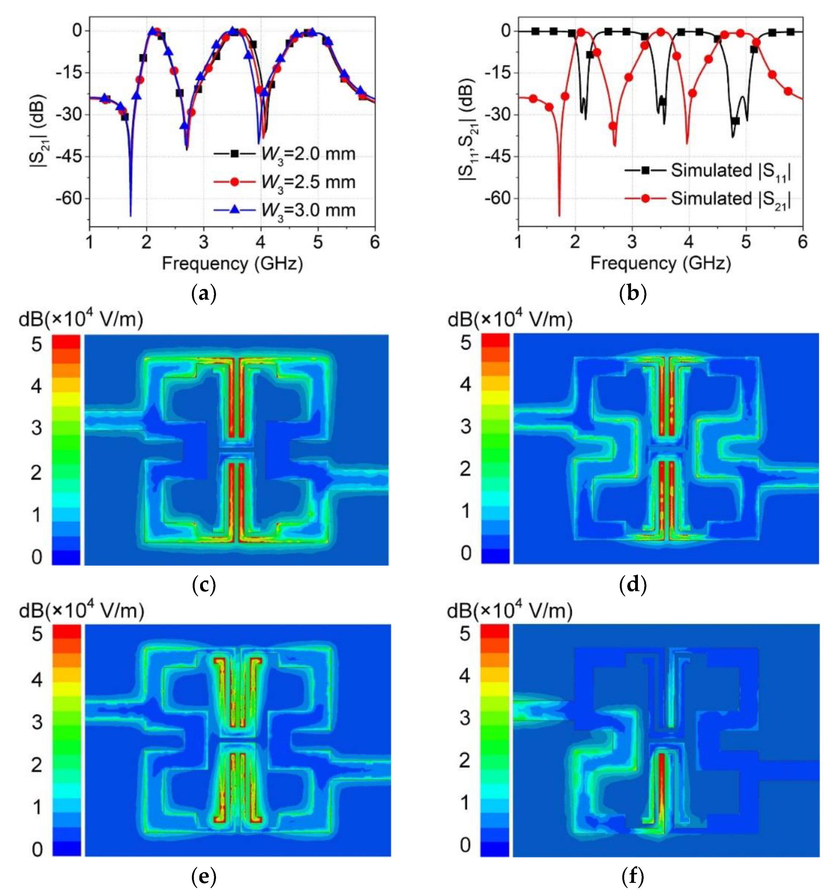
3.2. Tri-Wideband BPF Design

To construct a tri-wideband BPF with little increase in the physical size of the filter, a pair of FUIRs are folded into a suitable structure and placed inside the dual-wideband BPF. The FUIRs are fed by FOLSIRs to generate the required resonant frequency of 4.9 GHz. In the dual-wideband BPF, the second spurious resonant frequency of the FOLSIR is suppressed by a TZ to increase the width of the upper stopband. However, the second spurious resonant frequency of the FOLSIR is used to enlarge the bandwidth of the third passband because it is near 4.9 GHz [12]. The schematic diagram of the tri-wideband BPF is shown in Figure 5.
In order to place another pair of resonators and ensure that the structure of the FOLSIRs do not change, the size of L22 is decreased while L21 is increased. Therefore, the TZ produced by the electrical coupling path of FOLSIRs disappears. The CF of the second passband can still be tuned by adjusting the size of W3; as shown in Figure 6a, when W3 is increased, the CF of the second passband is decreased. In addition, by optimizing the tapping position t, length of L11 and L21, and width of the folded portion W3, the three passbands are adjusted to the expected position. After optimization, the full-wave EM simulation result of the tri-wideband BPF is shown in Figure 6b. The simulated |S21, S11| response exhibits three TZs, low insertion loss, high return loss, steep passband edges, and three wide passbands covering 2.035–2.305/3.31–3.71/4.54–5.18 GHz.
The simulated electric fields distributions of a tri-wideband BPF at 2.14 GHz, 3.5 GHz, 4.9 GHz, and 4 GHz are shown in Figure 6c, Figure 6d, Figure 6e, and Figure 6f, respectively. In the passbands, signals at 2.14 GHz, 3.5 GHz, and 4.9 GHz can pass through the tri-wideband BPF with little loss. On the other hand, the signal at 4 GHz is suppressed in the transmission line, for in the stopband. The simulation results of the electric fields’ distributions show that the tri-wideband BPF has effective signal selection performance for the propagated signal.

4. Manufacture and Measurement

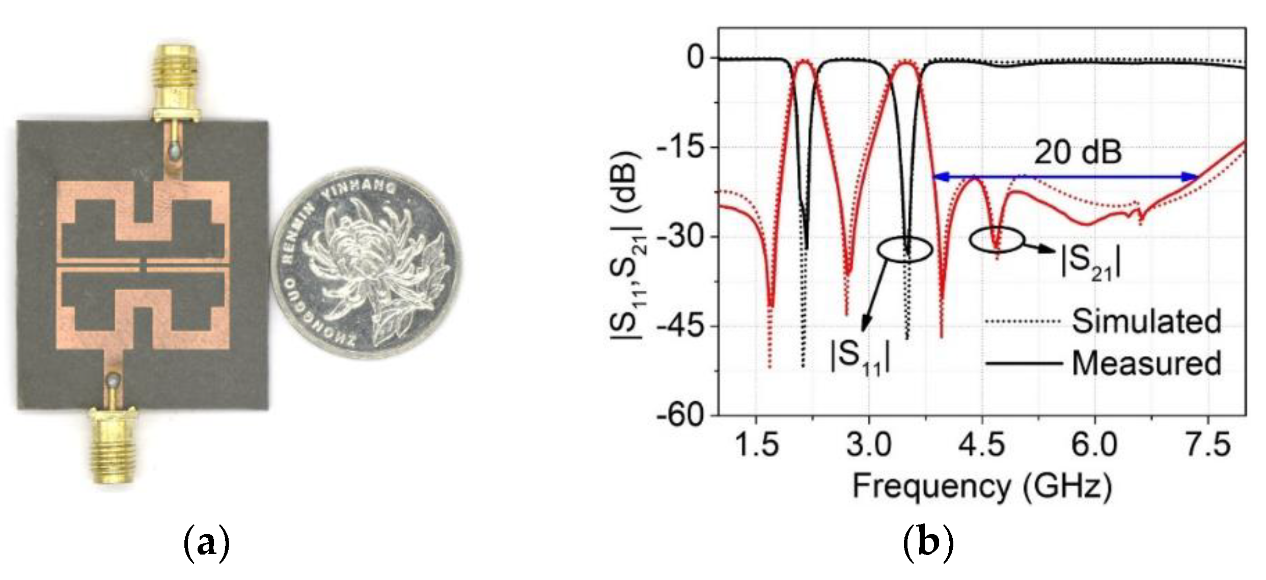
4.1. Dual-Wideband BPF Manufacture and Measurement

The proposed dual-wideband BPF without defective ground structures (DGSs) or vias is produced by laser engraving [41], and two SMA connectors are used to connect the I/O lines and ground, as shown in Figure 7a. Measurement of the fabricated dual-wideband BPF shows a compact size of 0.214λg × 0.22λg (or 21.9 mm × 22.5 mm), λg is the guided wavelength at the CF of the first passband. Through SMA connectors, the fabricated dual-wideband BPF is connected to the network analyzer (PNA, Agilent N5247A) to measure the S-parameters.
Figure 7b shows the very closed simulated and measured |S21, S11| response of the dual-wideband BPF. The measured result shows that the fabricated dual-wideband BPF has two passbands with CFs of 2.13 GHz and 3.47 GHz, a 3 dB fractional bandwidth (FBW) of 14% and 11.2%. What’s more, the two passbands have an insertion loss of 0.73 dB and 0.9 dB, and a return loss of 32 dB and 33 dB at CFs, respectively. Among two passbands, four TZs that are located at 1.72, 2.71, 3.97, and 4.69 GHz can be observed to improve the band-to-band isolation and out-of-band rejection level. The fabricated dual-wideband BPF has a 20 dB rejection upper stopband from 3.85 GHz to 7.39 GHz, which made the second harmonic suppression level of both passbands larger than 20 dB.
Table 1 shows a performance comparison of the proposed dual-wideband BPF in this paper with some referenced dual-band BPFs. It is seen that our filters tend to show better bandwidth performance that the filters in the references with the same size level. In addition, the insertion losses remain the lowest value among the counterparts. After the comparison, it can be proved that the dual-wideband BPF proposed in this work shows better bandwidth and insertion loss. Some research studies in the literature have proposed filters covering sub-6 GHz bands of 5G [19,32,33,37], but they all have smaller bandwidth and larger insertion loss. In [32], a dual-band BPF covering two 5G bands was proposed. The tri-wideband BPF proposed in this paper operates the same two bands, comparing with which, the dual-band BPF proposed in [32] has a larger size and shows smaller bandwidths. Moreover, using the laser-engraving to process microstrip devices without DGSs or vias can effectively reduce the process cost and improve the production efficiency.
The sizes listed in Table 1 and Table 2 are dimensionless values, which are coefficients of λg × λg, and they are the products of the ratios of the absolute sizes of the filters’ edges to λg.

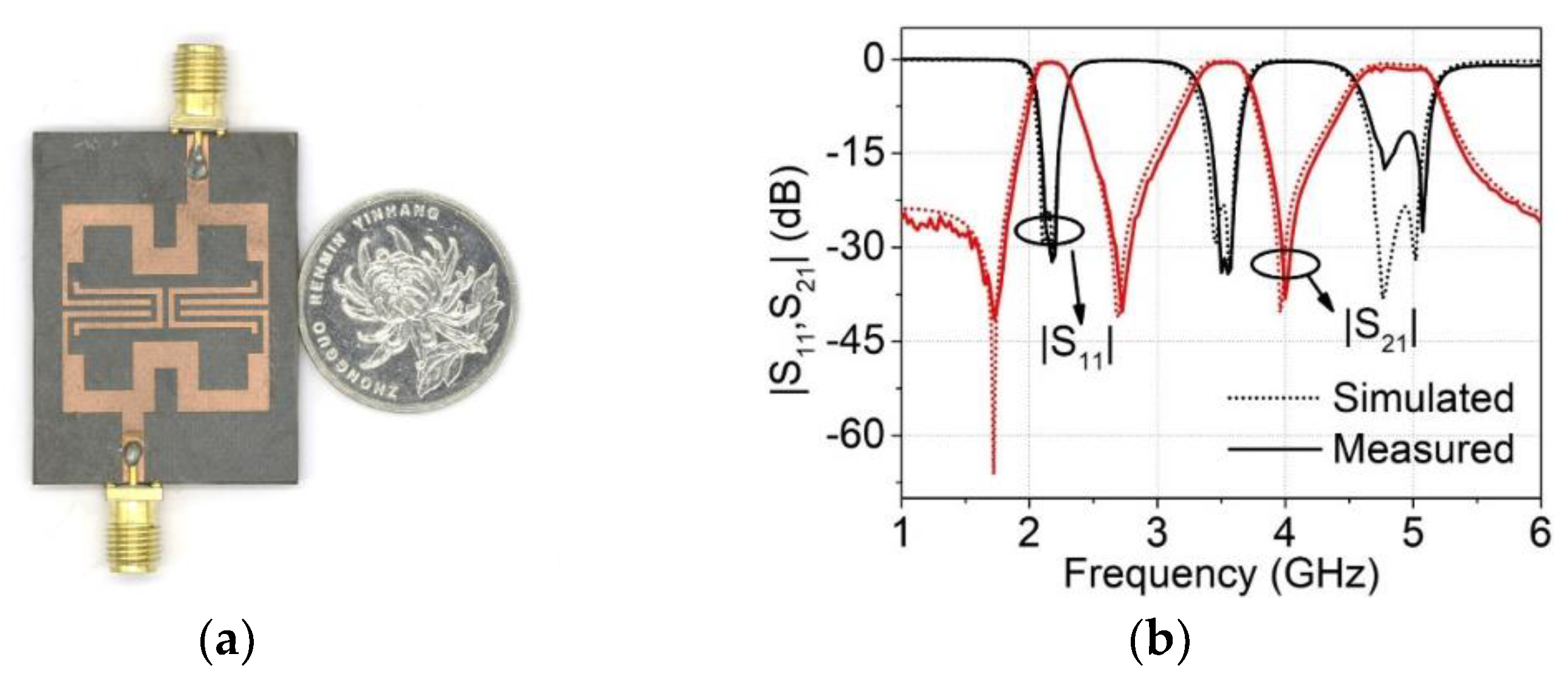
4.2. Tri-Wideband BPF Manufacture and Measurement

The tri-wideband BPF produced by laser-engraving is shown in Figure 8a. The tri-wideband BPF has a compact size of 0.225λg × 0.226λg (or 23.1 mm × 23.2 mm) and a simple structure without DGSs or vias to reduce the production cost. Two SMA connectors are used to connect the I/O lines and ground. Figure 8b shows the simulated and measured |S21, S11| response of the tri-wideband BPF, which are quite consistent with each other. The measured result shows that the three passbands centered at 2.17, 3.51, and 4.86 GHz and with 3 dB FBWs of 12.4%, 11.4%, and 13.3%. The passbands have measured insertion losses of 0.46, 0.49, and 1.3 dB and return losses of 32.3, 33, and 11.6 dB at the CF, respectively. Among two passbands, three TZs located at 1.72, 2.71, and 4 GHz can be observed, which can improve the band-to-band isolation and out-of-band rejection.
Table 2 gives the performance comparison results of the tri-wideband BPF proposed in this paper and tri-band BPFs in the references. It can be easily seen from the comparison results that the tri-wideband BPF proposed in this paper has better bandwidth and insertion loss than the counterparts with same dimensions. A compact tri-band BPF proposed in [29] has a competitive bandwidth performance; however, all its three passbands show large insertion loss. Furthermore, the tri-wideband BPF still has a simple structure without DGSs or vias, which is processed with low cost and high production efficiency by laser engraving.

5. Conclusions

This work proposed a FOLSIR with a higher degree of resonant frequency tuning freedom, a controllable TZ, and compact structure, based on which a dual-wideband BPF has been designed. By adding a pair of resonators inside the dual-wideband BPF, a tri-wideband BPF is obtained with almost no increase in the physical size of the filter. Both the dual-wideband BPF and tri-wideband BPF operate wide passbands adapted to 5G mobile communications. A novel passband adjustment method is proposed, which can freely increase or decrease the CF of the adjusted passband, and solve the limitation of the traditional adjustment method of loading stubs. Cross-coupling of the resonators generates more TZs to improve the band-to-band isolation and out-of-band rejection level. By adjusting the position of a TZ to suppress the spurious response, the second harmonic suppression level of both passbands of the dual-wideband BPF is larger than 20 dB. The two multi-wideband BPFs with the advantages of low insertion loss, steep passband edges, high out-of-band rejection, and compact size cover the sub-6 GHz bands of 5G mobile communications and the commonly used spectrum, which demonstrate that this research has great significance to 5G mobile communications.

Author Contributions

Conceptualization, Z.H. and C.L.; writing—original draft preparation, Z.H.; writing—review and editing, J.Z., D.H., B.Z., and R.S.; supervision, C.L.; project administration, Z.W. All authors have read and agreed to the published version of the manuscript.

Funding

This research was funded by National Natural Science Foundation of China (NSFC), grant number 11973034 and the National Key Laboratory of Electromagnetic Environment, China, grant number 6142403180101.

Conflicts of Interest

The authors declare no conflict of interest.

References

  1. The 5G Infrastructure Public Private Partnership (5G PPP). View on 5G Architecture, 2016. Available online: https://5g-ppp.eu/wp-content/uploads/2014/02/5G-PPP-5G-Architecture-WP-July-2016.pdf (accessed on 20 December 2019).
  2. Wu, S.; Razavi, B. A 900-MHz/1.8-GHz CMOS receiver for dual-band applications. IEEE J. Solid State Circuits 1998, 33, 2178–2185. [Google Scholar] [CrossRef]
  3. Shi, L.; Gao, J. Multitransmission Zero Dual-Band Bandpass Filter Using Nonresonating Node for 5G Millimetre-Wave Application. Act. Passiv. Electron. Compon. 2018, 2018. [Google Scholar] [CrossRef]
  4. Xu, J.; Wu, W.; Miao, C. Compact microstrip dual-/tri-/quad-band bandpass filter using open stubs loaded shorted stepped-impedance resonator. IEEE Trans. Microw. Theory Tech. 2013, 61, 3187–3199. [Google Scholar] [CrossRef]
  5. Luo, S.; Zhu, L.; Sun, S. Compact dual-mode triple-band bandpass filters using three pairs of degenerate modes in a ring resonator. IEEE Trans. Microw. Theory Tech. 2011, 59, 1222–1229. [Google Scholar]
  6. Sun, S.J.; Su, T.; Deng, K.; Wu, B.; Liang, C.H. Shorted-ended stepped-impedance dual-resonance resonator and its application to bandpass filters. IEEE Trans. Microw. Theory Tech. 2013, 61, 3209–3215. [Google Scholar] [CrossRef]
  7. Zhang, R.; Zhu, L.; Luo, S. Dual-mode dual-band bandpass filters with adjustable frequency ratiousing an annular ring resonator. IEEE Microw. Wirel. Compon. Lett. 2013, 23, 13–15. [Google Scholar] [CrossRef]
  8. Luo, S.; Zhu, L.; Sun, S. A dual-band ring-resonator bandpass filter based on two pairs of degenerate modes. IEEE Trans. Microw. Theory Tech. 2010, 58, 3427–3432. [Google Scholar] [CrossRef]
  9. Liu, H.; Lei, J.; Zhao, Y.; Li, S.; Guan, X. Compact triple-band bandpass filter using multimode stubs loaded resonator. Microw. Opt. Technol. Lett. 2013, 55, 2672–2675. [Google Scholar] [CrossRef]
  10. Tantiviwat, S.; Ibrahim, S.Z.; Razalli, M.S. Design of quad-channel diplexer and tri-band bandpass filter based on multiple-mode stub-loaded resonators. Radioengineering 2019, 27, 129–135. [Google Scholar] [CrossRef]
  11. Yu, B.; Jia, B.; Zhu, Z. A compact tri-band bandpass filter using novel stub-loaded resonator. Microw. Opt. Technol. Lett. 2015, 57, 2797–2800. [Google Scholar] [CrossRef]
  12. Gao, L.; Zhang, X.Y.; Xue, Q. Compact Tri-Band Bandpass Filter Using Novel Eight-Mode Resonator for 5G WiFi Application. IEEE Microw. Wirel. Compon. Lett. 2015, 25, 660–662. [Google Scholar] [CrossRef]
  13. Cho, Y.H.; Yun, S.W. A tri-band bandpass filter using stub-loaded SIRs with controllable bandwidths. Microw. Opt. Technol. Lett. 2014, 56, 2907–2910. [Google Scholar] [CrossRef]
  14. Ren, B.; Ma, Z.; Liu, H.; Guan, X.; Wen, P.; Wang, X.; Masataka, O. Miniature dual-band bandpass filter using modified quarter-wavelength SIRs with controllable passbands. Electron. Lett. 2018, 55, 38–40. [Google Scholar] [CrossRef]
  15. Gomez-Garcia, R.; Yang, L.; Munoz-Ferreras, J.M.; Psychogiou, D. Selectivity-Enhancement Technique for Stepped-Impedance-Resonator Dual-Passband Filters. IEEE Microw. Wirel. Compon. Lett. 2019, 29, 453–455. [Google Scholar] [CrossRef]
  16. Li, C.Y.; Chen, J.X.; Tang, H.; Zhou, L.H.; Shi, J.; Bao, Z.H. Tri-band bandpass filter with wide stop-band using stub-loaded triple-mode resonator. J. Electromagn. Waves Appl. 2013, 27, 439–447. [Google Scholar] [CrossRef]
  17. Chen, F.; Qiu, J.; Chu, Q. Design of compact tri-band bandpass filter using centrally loaded resonators. Microw. Opt. Technol. Lett. 2013, 55, 2695–2699. [Google Scholar] [CrossRef]
  18. Zhang, X.Y.; Chen, J.-X.; Xu, Q.; Li, S.-M. Dual-Band Bandpass Filters Using Stub-loaded Resonators. IEEE Microw. Wirel. Compon. Lett. 2007, 17, 583–585. [Google Scholar] [CrossRef]
  19. Chen, F.; Chu, Q.; Tu, Z. Design of compact dual-band bandpass filter using short stub loaded resonator. Microw. Opt. Technol. Lett. 2009, 51, 959–963. [Google Scholar] [CrossRef]
  20. Wu, X.; Chu, Q.; Tian, X. Dual-band bandpass filter using novel side-stub-loaded resonator. Microw. Opt. Technol. Lett. 2012, 54, 362–364. [Google Scholar] [CrossRef]
  21. Liu, Y.; Zhao, Y.J.; Zhou, Y.G.; Niu, Z.Y. Integrated dual-band BPF and single-band BSF for tri-band filter design. J. Electromagn. Waves Appl. 2011, 25, 2420–2428. [Google Scholar] [CrossRef]
  22. Huang, J.; Wen, J.; Lyu, Z. A triple broadband microwave filter synthesis using nonuniform lines. Microw. Opt. Technol. Lett. 2008, 50, 3039–3045. [Google Scholar] [CrossRef]
  23. Xu, J.; Zhu, Y. Compact semi-lumped dual- and tri-wideband bandpass filters. IET Microw. Antennas Propag. 2017, 11, 53–58. [Google Scholar] [CrossRef]
  24. Xu, K.; Zhang, Y.; Li, D.; Fan, Y.; Li, J.L.W.; Joines, W.T.; Liu, Q.H. Novel design of a compact triple-band bandpass filter using short stub-loaded SIRs and embedded SIRs structure. Prog. Electromagn. Res. 2013, 142, 309–320. [Google Scholar] [CrossRef] [Green Version]
  25. Gong, L.; Xiong, Y.; Zhang, F.; Wang, L.; Sun, Y.; Zhao, X.; He, M.; Ji, L.; Zhang, X.; Zhang, B. A triple-wideband bandpass filter with controllable bandwidths based on stub-loaded resonators. Int. J. Microw. Wirel. Technol. 2018, 10, 904–910. [Google Scholar] [CrossRef]
  26. Wang, Z.J.; Wang, C.; Kim, N.Y. Dual-/triple-wideband microstrip bandpass filter using independent triple-mode stub-loaded resonator. Microw. Opt. Technol. Lett. 2018, 60, 56–64. [Google Scholar] [CrossRef]
  27. Zhang, S.; Zhu, L. Compact tri-band bandpass filter based on λ/4 resonators with U-folded coupled-line. IEEE Microw. Wirel. Compon. Lett. 2013, 23, 258–260. [Google Scholar] [CrossRef]
  28. Song, Y.; Xu, Y.; Liu, H.; Ma, Z. Design of triple-band bandpass filter using quad-mode stepped impedance resonator (SIR) with shorted stub. IEICE Electron. Express 2018, 15, 20171219. [Google Scholar] [CrossRef] [Green Version]
  29. Chu, Q.X.; Wu, X.H.; Chen, F.C. Novel compact tri-band bandpass filter with controllable bandwidths. IEEE Microw. Wirel. Compon. Lett. 2011, 21, 655–657. [Google Scholar] [CrossRef]
  30. Chen, C.F.; Huang, T.Y.; Wu, R.B. Design of dual- and triple-passband filters using alternately cascaded multiband resonators. IEEE Trans. Microw. Theory Tech. 2006, 54, 3550–3558. [Google Scholar] [CrossRef]
  31. GaoDing, N. A controllable compact dual-band bandpass filter using loaded open-loop resonators. IEICE Electron. Express 2016, 13, 20160470. [Google Scholar] [CrossRef] [Green Version]
  32. Liu, L.; Fu, Q.; Liang, F.; Zhao, S. Dual-band filter based on air-filled SIW cavity for 5G application. Microw. Opt. Technol. Lett. 2019, 61, 2599–2606. [Google Scholar] [CrossRef]
  33. Wang, J.; Guan, Y.; Yu, H.; Li, N.; Wang, S.; Shen, C.; Dai, Z.; Gan, D.; Yang, R.; He, S.; et al. Transparent graphene microstrip filters for wireless communications. J. Phys. D. Appl. Phys. 2017, 50, 34LT01. [Google Scholar] [CrossRef]
  34. Li, Q.; Zhang, Y.H.; Feng, X.; Fan, Y. Tri-band filter with multiple transmission zeros and controllable bandwidths. Int. J. Microw. Wirel. Technol. 2016, 8, 9–13. [Google Scholar] [CrossRef]
  35. Li, X.; Zhang, Y.; Zhang, X.; Qu, L.; Yong, F. Compact quint-band Bandpass Filter design in a rigorous manner utilizing multimode stub-loaded taper. Microw. Opt. Technol. Lett. 2018, 60, 1230–1234. [Google Scholar] [CrossRef]
  36. Gan, D.; He, S.; Dai, Z.; Wang, J. A quad-band bandpass filter using split-ring based on T-shaped stub-loaded step-impedance resonators. Microw. Opt. Technol. Lett. 2017, 59, 2098–2104. [Google Scholar] [CrossRef]
  37. Denis, B.; Song, K.; Zhang, F. Compact dual-band bandpass filter using open stub-loaded stepped impedance resonator with cross-slots. Int. J. Microw. Wirel. Technol. 2017, 9, 269–274. [Google Scholar] [CrossRef]
  38. Chu, Q.-X.; Chen, F.-C. A compact dual-band bandpass filter using meandering stepped impedance resonators. IEEE Microw. Wirel. Compon. Lett. 2008, 18, 320–322. [Google Scholar]
  39. Ma, K.; Ma, J.G.; Yeo, K.S.; Do, M.A. A compact size coupling controllable filter with separate electric and magnetic coupling paths. IEEE Trans. Microw. Theory Tech. 2006, 54, 1113–1119. [Google Scholar]
  40. Hong, J.S. Microstrip Filters for RF/Microwave Applications, 2nd ed.; John Wiley and Sons: Hoboken, NJ, USA, 2011; ISBN 9780470408773. [Google Scholar]
  41. Zhou, W.; Liu, C.; Huang, G.L.; Xia, W.; Zhang, J.; He, D.; Wu, Z. Design and manufacture of lowpass microstrip filter with high conductivity graphene films. Microw. Opt. Technol. Lett. 2019, 61, 972–978. [Google Scholar] [CrossRef]
  42. Li, K.; Kang, G.; Liu, H.; Zhao, Z. High-selectivity adjustable dual-band bandpass filter using a quantic- mode resonator. Microsyst. Technol. 2019, 8, 1–4. [Google Scholar] [CrossRef]
Figure 1. Design of folded open-loop stepped-impedance resonators (FOLSIR). (a) Schematic diagram of stepped-impedance resonators (SIR); (b) The equivalent circuit diagram of the SIR; (c) Schematic diagram of FOLSIR; (d) The equivalent circuit diagram of the FOLSIR; (e) The simulated resonant frequency f0 and fS1 of the FOLSIR for various values of W3; (f) The simulated |S21| response of the resonator for various values of S1.
Electronics 09 00205 g001
Figure 2. Design of the folded uniform impedance resonator (FUIR). (a) Schematic diagram of the FUIR; (b) The simulated resonant frequency of the FUIR for various values of W5.
Electronics 09 00205 g002
Figure 3. Schematic diagram of dual-wideband bandpass filters (BPF).
Electronics 09 00205 g003
Figure 4. Simulation of dual-wideband bandpass filters (BPF). (a) The simulated |S21| response of the filter for various widths of W3; (b) The simulated |S21| response of the filter for various widths of S; (c) The simulated |S21| response of the filter for various widths of S1; (d) Simulated |S21, S11| response of the dual-wideband BPF; (e) The simulated electric fields distributions of the dual-wideband BPF at 2.14 GHz; (f) The simulated electric fields distributions of the dual-wideband BPF at 2.68 GHz; (g) The simulated electric fields distributions of the dual-wideband BPF at 3.5 GHz.
Electronics 09 00205 g004
Figure 5. Schematic diagram of tri-wideband BPF.
Electronics 09 00205 g005
Figure 6. Simulation of a tri-wideband BPF. (a) The simulated |S21| response of the filter for various values of W3; (b) Simulated |S21, S11| response of the tri-wideband BPF; (c) The simulated electric fields distributions of a tri-wideband BPF at 2.14 GHz; (d) The simulated electric fields distributions of a tri-wideband BPF at 3.5 GHz; (e) The simulated electric fields distributions of a tri-wideband BPF at 4.9 GHz; (f) The simulated electric fields distributions of a tri-wideband BPF at 4 GHz.
Electronics 09 00205 g006
Figure 7. Manufacture and measurement of the dual-wideband BPF. (a) Photograph of the dual-wideband BPF; (b) Simulated and measured |S21, S11| response of the dual-wideband BPF.
Electronics 09 00205 g007
Figure 8. Manufacture and measurement of the dual-wideband BPF. (a) The photograph of a dual-wideband BPF; (b) The simulated and measured |S21, S11| response of the dual-wideband BPF.
Electronics 09 00205 g008
Table 1. Performance comparison with other dual-band BPFs. CF: center frequencies, DGS: defective ground structures, FBW: fractional bandwidth. IL: insertion loss. RL: return loss.
CF(GHz)FBW(%)IL(dB)RL(dB)Size
(λg × λg)
DGSs or Vias
[8]2.38/4.876.7/82/1.4--No
[18]1.84/2.98.1/6.81.7/1.6>10-No
[19]2.4/3.59.6/61.4/1.3515.3/16.20.0306Yes
[31]3/5.3410/3.70.19/2.34-0.039No
[32]3.5/4.95.4/2.20.75/1.3-1.9803Yes
[33]3.4/6.74.8/43.8/3.718.7/14.6-No
[37]2.4/3.59.6/7.71.42/1.1925/20.10.482No
[42]2.3/3.211.3/9.41.1/1.740/12.00.228No
This Work2.13/3.4714/11.20.73/0.932/330.0471No
Table 2. Performance comparison with other tri-band BPFs.
CF(GHz)FBW(%)IL(dB)RL(dB)Size
(λg × λg)
DGSs or Vias
[6]1.5/2.45/3.57.5/5.8/3.61.17/1.02/2.17>170.0308Yes
[10]1.75/2.45/3.55.7/4.1/5.71.4/1.9/1.9>120.036Yes
[13]1.57/2.4/3.512.9/8.1/4.60.6/1/2.413/500.0988Yes
[17]1.57/2.45/5.26.8/7.8/8.061.2/1.2/1.3>170.0276Yes
[24]2.45/3.5/5.29.6/13.1/7.91.2/1.5/1.616.3/17.9/12.90.0486Yes
[27]1.8/3.5/5.87/5/3.50.88/1.33/1.7721.3/15.84/15.720.0572Yes
[29]2.41/3.56/5.296.2/12.2/11.81.9/1.42/1.5114.3/15/16.80.0255Yes
[30]2.5/3.6/5.14.0/4.0/6.02.9/2.7/2.3>170.1716No
[34]1.8/2.4/5.88.9/12.5/5.31.5/0.9/2.915/23/190.0272Yes
This Work2.17/3.51/4.8612.4/11.4/13.30.46/0.49/1.332/33/11.60.0508No

