1. Introduction
The DC (direct current) transformer is a necessary link for interconnecting DC networks of different voltage levels. It has been widely used in the field of new energy, fuel cells, supercapacitors, and where there are a DC bus and unidirectional transmission of energy in servers and communications [
1,
2]. To achieve high efficiency and high-power density DC transformers, many scholars have done a lot of research. Though the topology of the LCL (inductor–capacitor–inductor) resonant DC transformer is simple, it requires a large inductor on the DC side, which increases the cost, size, and weight of the converter. This type of DC transformer has no electrical isolation, which makes it easy to cause power reflow, and the probability of causing an electric shock accident is greatly increased. Therefore, more attention has been paid to DC transformers with electrical isolation. The dual active bridge (DAB) converter has a simple structure, can achieve soft switching (ZVS) characteristics, and energy flows in both directions [
3,
4]. However, its ZVS range is limited, and the switch also has a high turn-off current, resulting in a reduction in power conversion efficiency [
5]. Even if the performance of the circuit can be improved by other modulation strategies, the complexity of the system control will increase accordingly [
6]. The LLC resonant converter can achieve soft switching characteristics in the full load range and does not require complex control strategies [
7,
8]. Therefore, the research on the LLC converter has received extensive attention.
The LLC (inductor–inductor–capacitor) resonant converter can work in two modes: DC–DC converter with output voltage regulation under frequency modulation operation and DC transformer with fixed frequency operation whose output voltage changes with input. Literature [
9,
10] proposed the concept of parallel regulation. In those papers, the LLC resonant DCX (direct current transformer) and the PWM (pulse width modulation) DC–DC converter are cascaded to make the input side in series and the output side in parallel. Then, by processing the output power of the auxiliary parallel PWM DC–DC converter, the output voltage can be strictly regulated and the overall converter efficiency can be reduced. Similar to the above idea, literature [
11,
12] added an auxiliary transformer in the resonant cavity. The primary winding of the auxiliary transformer is connected in series with the main transformer, and the secondary winding is connected in parallel with the main transformer. Combined with the corresponding control, the LLC resonant converter works in DCX mode. However, the above methods all need to add additional circuits, which increases the volume of DCX.
To ensure that the LLC resonant converter always works at the optimal frequency, it must be ensured that the LLC resonant converter operates at the same frequency as the resonant frequency [
13]. However, for LLC resonant converters operating under fixed frequency conditions, it is difficult to ensure that they work at the optimal frequency at all times. In actual industrial products, due to manufacturing processes and other reasons, the actual parameters of the LLC resonant converter resonant tank have a certain deviation from the set parameters. Due to the impact of changes in the actual operating environment of the LLC resonant converter, there are also differences between actual operating parameters and theoretical calculation parameters [
14]. Based on the above factors, it can be seen that the resonant frequency of the resonant converter changes dynamically under actual operation. To synchronize the operating frequency with the resonant frequency, it is necessary to add a frequency tracking control link to maximize the transmission efficiency of the circuit [
15,
16] and then perform voltage regulation through the cascaded PWM DC–DC converter. The frequency tracking of the circuit in [
15,
16] is based on the detection of the cavity current signal. However, the load in the actual circuit changes, which has a great influence on the resonant cavity current of the LLC resonant converter. When the load is light, the resonant cavity current does not change much, and the detection is difficult, which greatly affects the detection accuracy and brings certain uncertainty. The method of voltage detection is less affected by the load [
17,
18,
19]. The advantages and disadvantages of the detection methods mentioned above are summarized in
Table 1. However, the existing literature only proposes a frequency tracking method and does not analyze in detail the mechanism of the LLC DC transformer to achieve the optimal operating point for voltage sampling, and the impact of different operating conditions on the optimal operating point.
This paper analyses and summarizes the frequency tracking method of the LLC resonant converter in the existing paper, and proposes a new method of frequency tracking based on voltage detection, which solves the shortcoming of current detection in the current method that it is difficult to distinguish the working range of the circuit at light load. The influence of load and magnetizing inductor change on the optimal operating point of LLC resonant converter is analyzed, and a theoretical analysis is given. In
Section 2, modal analysis of the LLC resonant circuit is made for the three cases of
fs > fr,
fs < fr,
fs = fr. The characteristics of the voltage and current waveforms in the three cases are found. In
Section 3, this paper analyses the driving waveform of the primary side switch when operating below the optimal resonance point, the current waveform of the resonant circuit, the voltage waveform of the secondary side rectifier diode, and the output voltage waveform of the LLC resonant DC transformer, and the implementation method of adaptive frequency tracking strategy is given. In
Section 4, the influence of the manufacturing process in practice is considered, the influence of the change of output power and the change of the excitation inductor of the resonance tank on the optimal operating point of the circuit are analyzed. As outlined in
Section 5, the above analysis was simulated and verified, and then a 1 kW LLC resonant converter prototype was designed and built under laboratory conditions. The experiment proved the influence of load change on the optimal operating point of DCX and verified the adoption of the correctness of the control strategy.
2. Operational Analysis
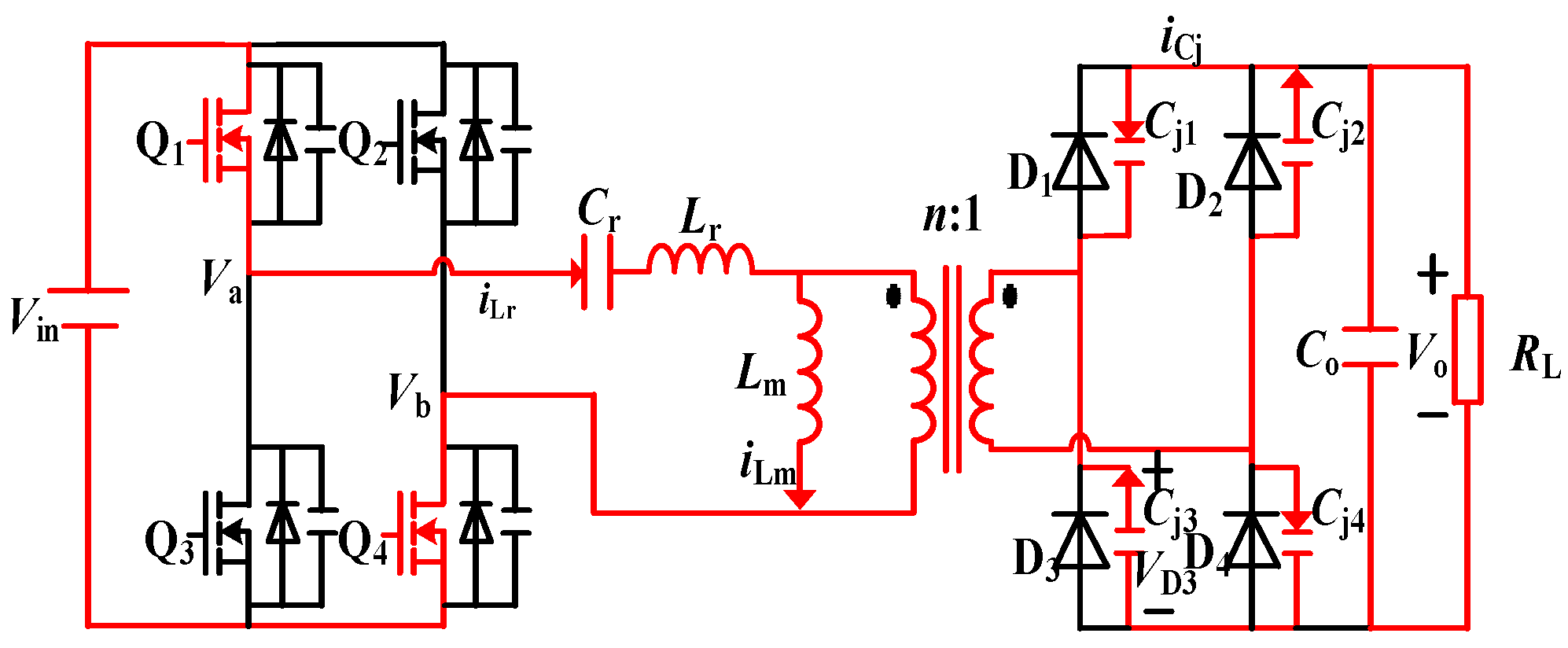
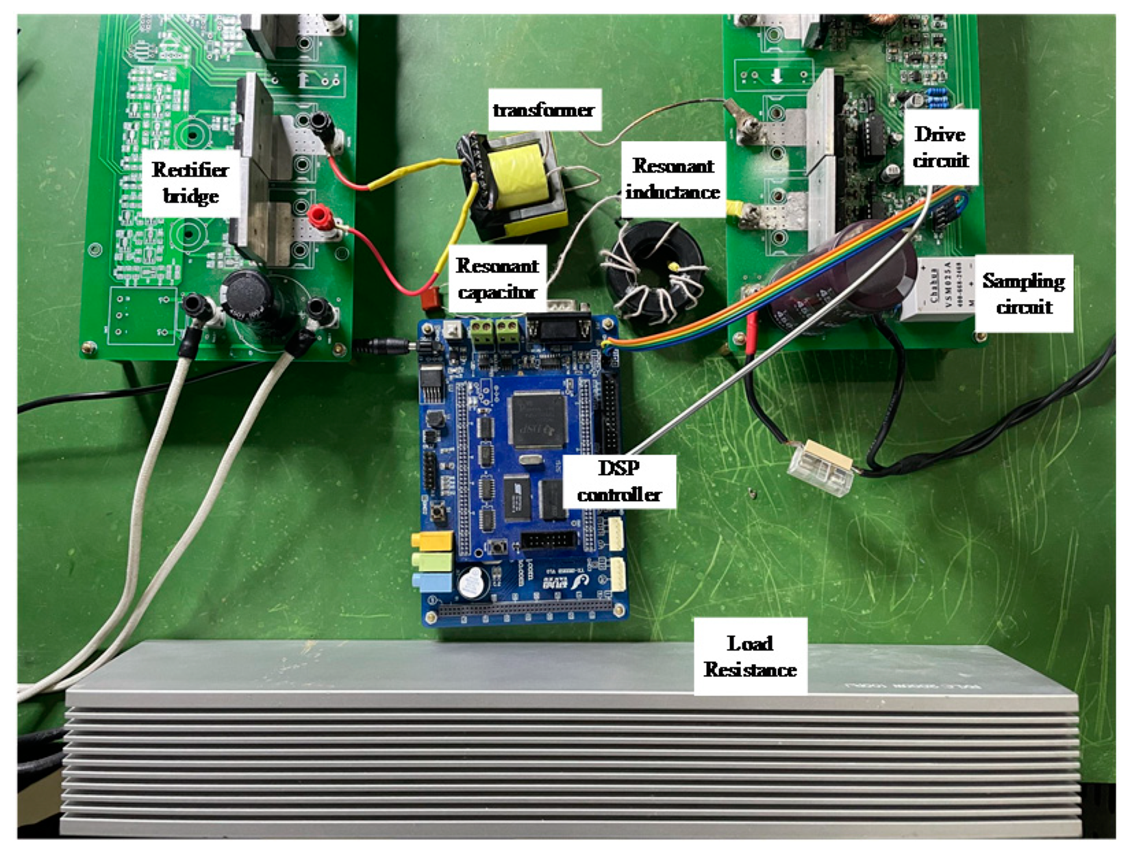
Figure 1 shows a full-bridge rectified LLC resonant converter.
Q1~
Q4 are primary switching transistors,
Lr is a resonant inductor,
Cr is a resonant capacitor,
Lm is a magnetizing inductor, and
D1~
D4 are output rectifier diodes. Unlike traditional PWM converters, LLC resonant converters adjust the output voltage by adjusting the switching frequency. When the converter operates in different frequency ranges, the secondary diode voltage and current waveforms will be different.
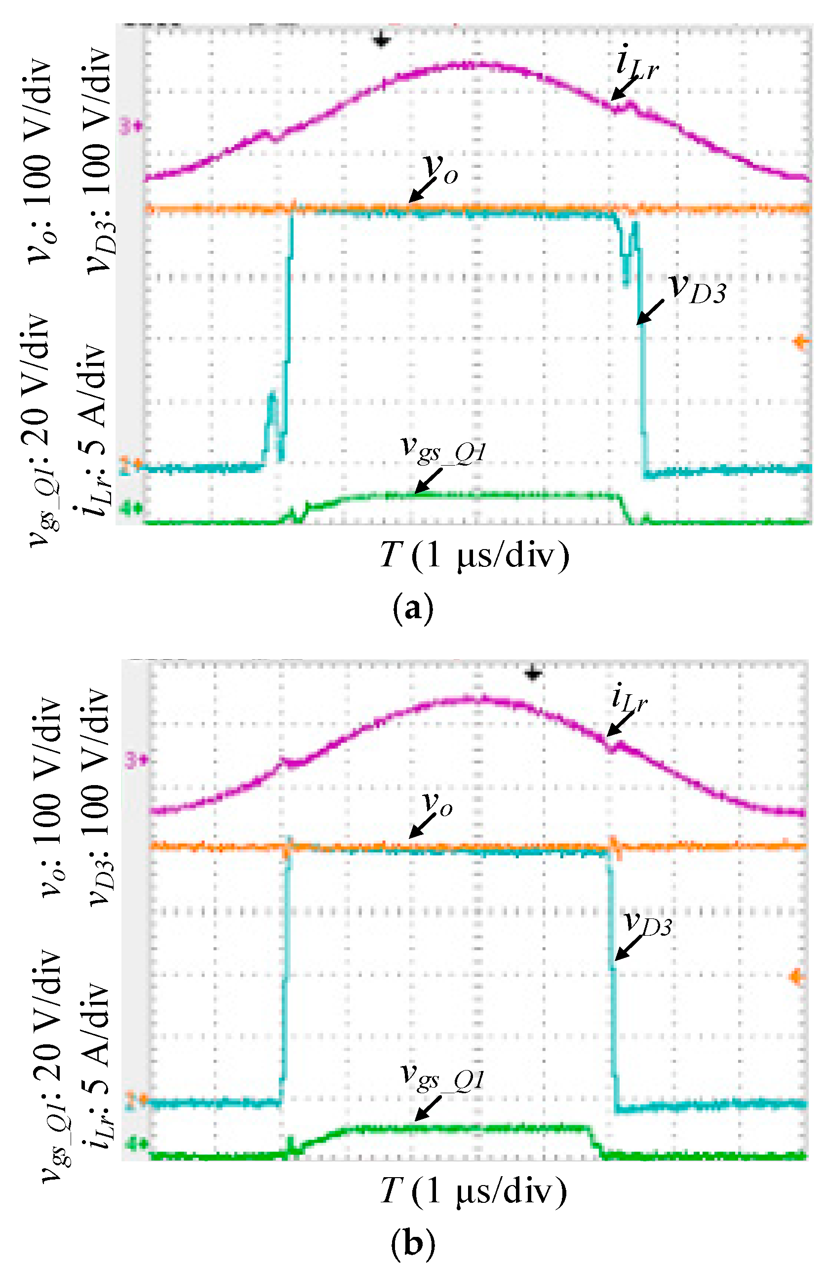
The main voltage and current waveforms of the LLC resonant converter for
fs < fr (
fs is the working frequency of switch,
fr is the resonant frequency of LLC converter) are shown in
Figure 2. At
t1, the resonance current
Ir and the excitation current
Im start to be equal, the secondary diodes
D1 and
D4 have a current of 0, and zero current shutdown can be achieved. At
t2, the primary switches
Q1 and
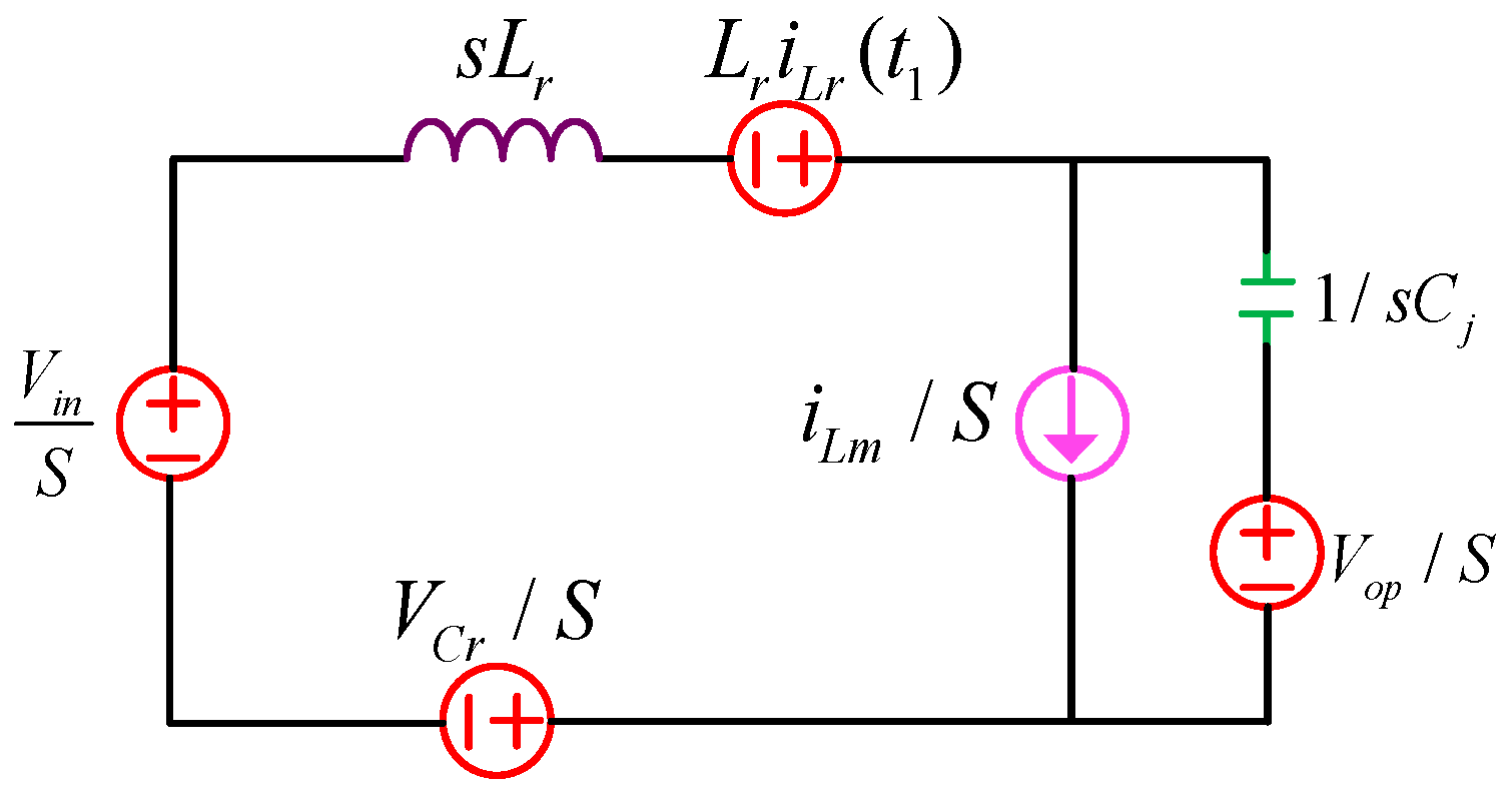
Q4 of the converter are turned off. During [
t1–t2], the voltage across the excitation inductor is not clamped by the output voltage and the converter enters a three-element resonance state. As the current through the diode drops to zero, the
D1 and
D4 junction capacitors are charged, the
D2 and
D3 junction capacitors are discharged, and the capacitor of the output rectifier diode resonates with the resonant inductor
Lr; the resonant current of the resonant circuit and the voltage across capacitor
D3 oscillate. Detailed analysis of the oscillation process is given in
Section 3 of this article. At the moment when the switches
Q1 and
Q4 are turned off, the diode voltage
VD3 across the rectifier
D3 is less than
Vo; the equivalent circuit diagram of this period is shown in
Figure 3. During [
t2–t3], the voltage
VD3 across the capacitor
D3 drops rapidly. At
t3,
VD3 drops to 0, the resonance inductor and the excitation inductor start to be unequal, the secondary rectifiers
D2 and
D3 start to conduct, and the next cycle is started. It can be known from the above analysis that when
fs < fr, the LLC resonant converter has two working modes during [
t1–t3].
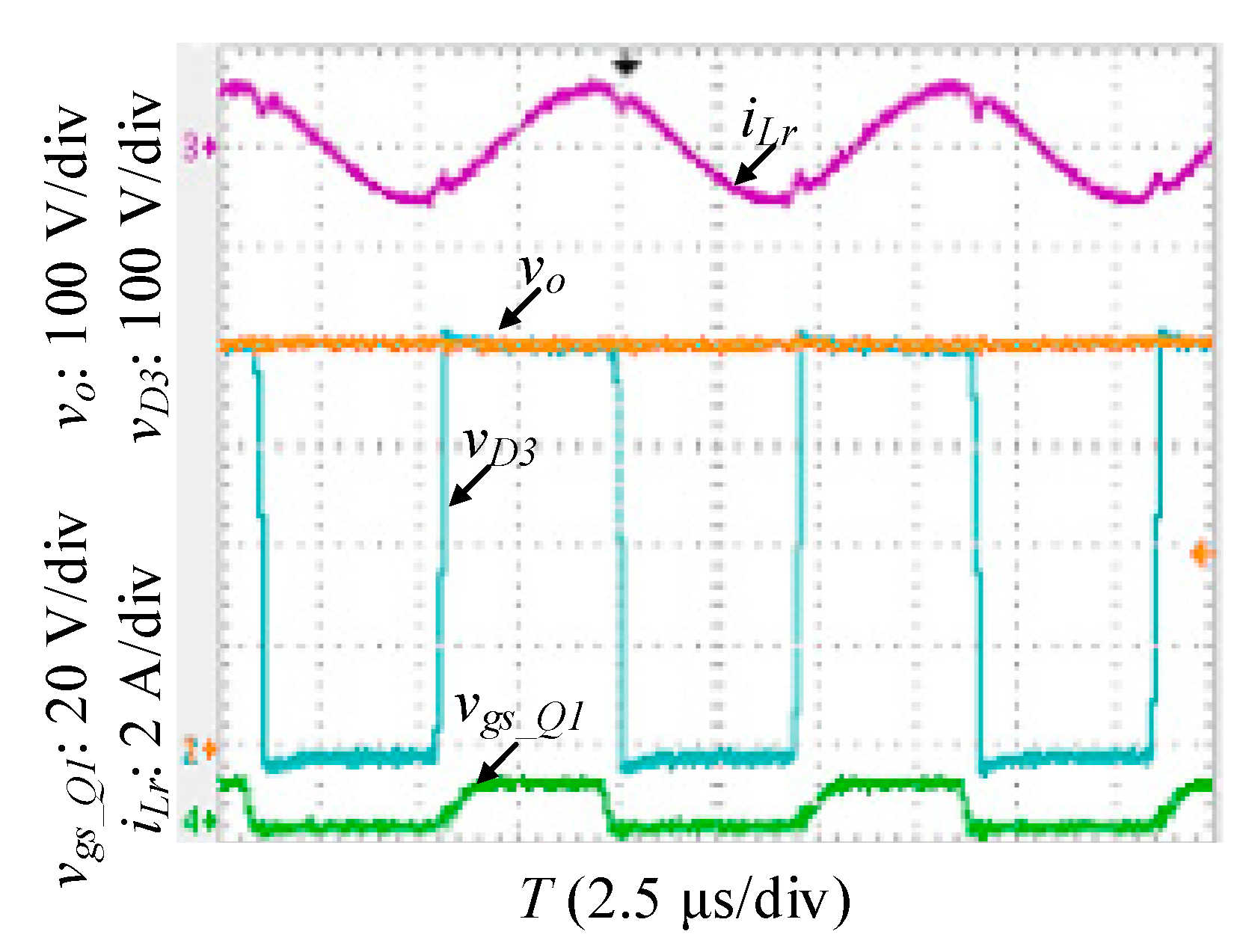
The main voltage and current waveforms of the LLC resonant converter for
fs > fr are shown in
Figure 4. Because the resonance period is smaller than the switching period, the resonance tank current
iLr curve cannot intersect with the excitation inductor current
iLm curve when the primary side switches
Q1 and
Q4 are closed at
t1, resulting in the current flowing through the rectifier diodes
D1 and
D4 not being zero, and the voltage
VD3 of the rectifier
D3 remaining at the output voltage
Vo. The excitation inductor voltage is affected by the output voltage clamping, and the excitation inductor current continues to increase for a short time. Because the switches
Q1 and
Q4 are closed, the bridge arm voltage
Vab becomes zero, and the resonance tank current drops rapidly. The equivalent circuit diagram for [
t1–t2] is shown in
Figure 5. At
t2, the resonance current
iLr and the excitation inductor current
iLm are equal, after which the voltage
VD3 of the rectifier
D3 drops rapidly, preparing for the output rectifier diode rectification. During [
t2–t3], the voltage
VD3 of the rectifier diode
D3 drops to 0 at
t3, the resonance inductance and the excitation inductance begin to be unequal, the rectifier diodes
D2 and
D3 start to conduct, and the next cycle begins. It works in the same way as
fs < fr in the period [
t2–
t3].
The main voltage and current waveforms of the LLC resonant converter for
fs = fr are shown in
Figure 6. At
t1, the primary side switches
Q1 and
Q4 are disconnected, and the resonance tank current
iLr and the excitation inductor current
iLm intersect. During [
t1–t2], the working mode is the same as the previous two cases during [
t2–t3]. Therefore, when
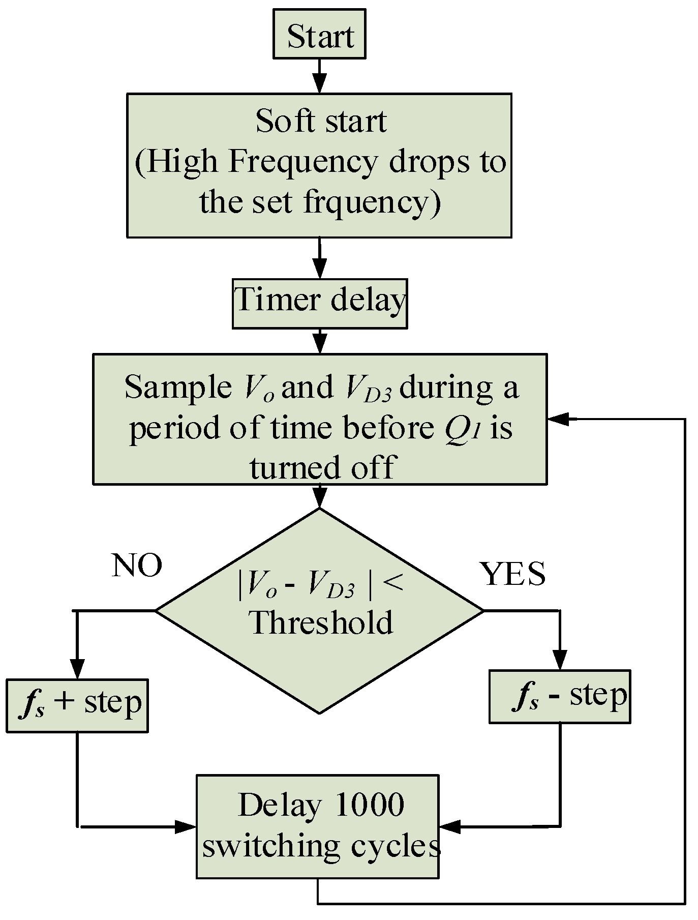
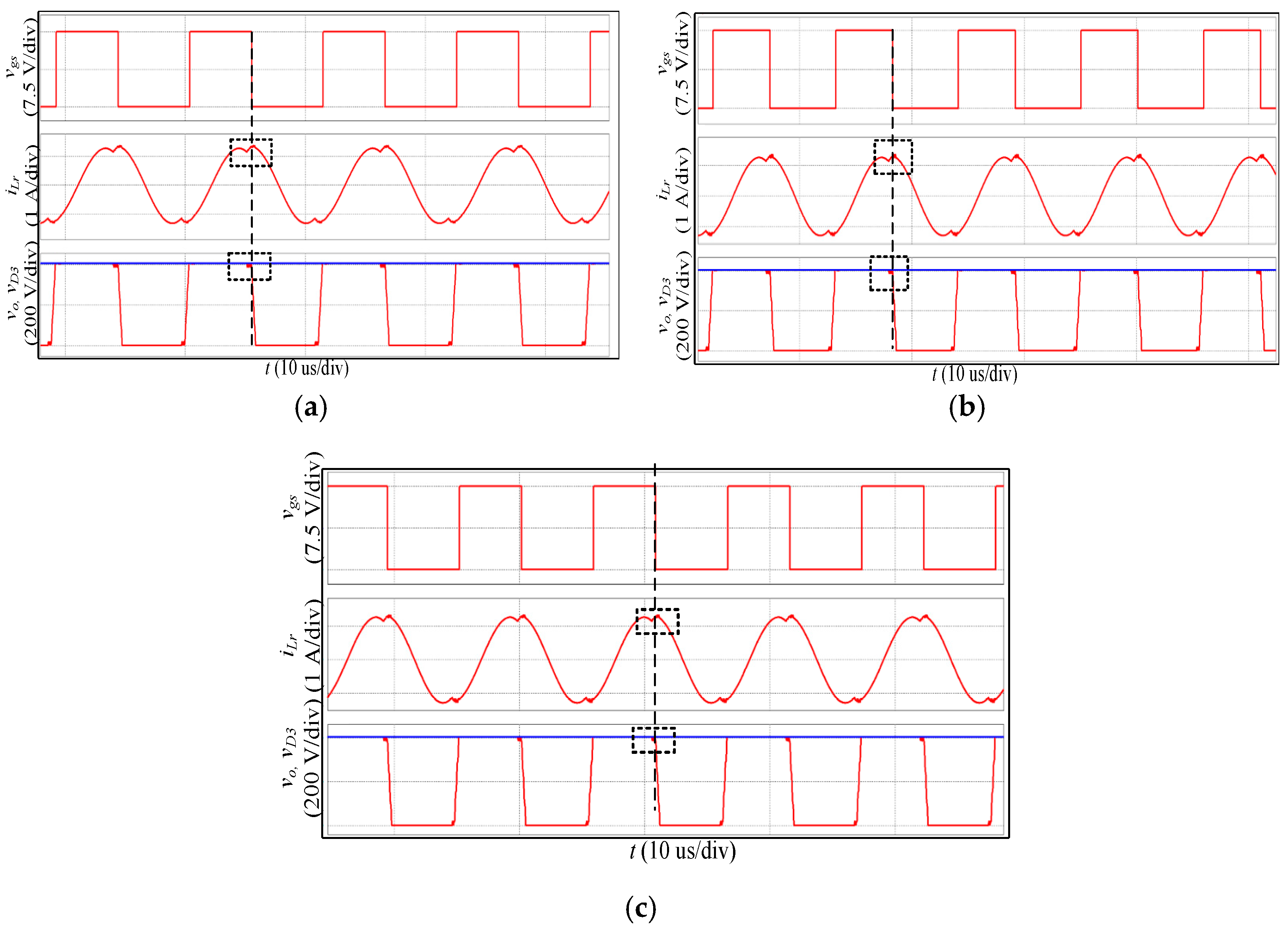
fs = fr, there is one less working mode than the first two cases. Through the above analysis, it can be seen that, when the LLC resonant converter works in different frequency ranges, the working model is slightly different. When the primary switch is turned off, the voltage on the output rectifier diode is different. Therefore, the frequency tracking control can be realized by judging the voltage of the rectifier diode when the switch is turned off.
According to the above analysis, when working below the resonant frequency (fs < fr), there is more circulating energy in the resonant tank, which causes the switch to conduct more RMS current and generate more conduction losses. When working below the resonant frequency (fs > fr), the primary side switch has a higher current when it is closed, which causes more switching losses. Therefore, when the LLC resonant converter operates at fs = fr, the working efficiency of the converter is the highest. When the LLC resonant converter is in a different frequency range, the voltage of the secondary side rectifier diode is different at the moment when the primary side switches Q1 and Q4 are cut off. When fs < fr, VD3 is less than Vo, and when fs > fr, VD3 is equal to Vo. Therefore, by judging the voltage on the rectifier diode D3 when the primary switches Q1 and Q4 are turned off, the best operating frequency can be tracked.
4. Analysis of the Influence of Frequency
Accurate analysis of LLC resonant converter will produce a very complex model; the process is more cumbersome. Therefore, to analyze the LLC resonant converter simply and effectively, the method currently used is the fundamental approximation method (first harmonic approximation; FHA). This method assumes that the energy transfer from the input to the output is mainly caused by the fundamental component of the voltage and current while ignoring other higher harmonic components that have little effect on the entire system.
First, the Fourier series expansion of the output voltage
Vab of the inverter bridge is [
20]:
In the Equation (10), fs = 1/Ts, Ts is the switching period.
The fundamental component of
Vab is:
Then the valid value of
Vab1 is:
Since the converter works at the resonance point, the resonance current can be expressed as:
where
is the phase difference between the resonance current and the excitation current and
is the phase difference between the input voltage and the resonance current.
The working waveform of the full-bridge LLC resonant converter for when the converter works at the resonance frequency point is shown in
Figure 13.
It can be seen from
Figure 13 that the fundamental component waveform of the input voltage and the waveform of the resonance current are almost the same at the resonance point. Since the dead time of the control circuit is fixed, and the dead time is much shorter than the switching period, it can be considered that the phase difference between the input voltage and the resonant current is approximately
.
It can be obtained from the above analysis that the input power of the entire circuit is:
The output power of the entire circuit is:
where
RL is the load resistor.
Ignoring the loss of the LLC resonant converter, according to the principle of energy conservation, the output power is equal to the input power.
It can be known from Equation (12) that the effective value of the input voltage is only related to the input voltage Vin and keeps the output voltage unchanged, according to Equation (16). Due to power conservation, when the load is doubled, the input voltage remains constant, and the effective value of the resonant current doubles.
It can also be seen from
Figure 14 that the excitation current and the resonance current are equal during the half-resonance period. The peak value of the excitation current at this time is:
At the same time, within half a resonance period, the difference between the average value of the resonance current and the excitation current is the average value of the output current converted to the primary side, establishing the following two equations:
In Equation (19),
To is the resonance period, and the relationship between
Ts and the dead time
Td is:
According to Equations (18) and (19), the expression of primary-side current effective value is:
The simultaneous Equations (16) and (21) can be expressed:
It can be known from Equation (22) that, when the parameters of the resonant converter are determined, the resonant period
To increases as the load increases. The trend is shown in
Figure 15. The relationship curve between power and resonance frequency is drawn in MATLAB as shown in
Figure 16. From that figure, it can be concluded that the resonance frequency decreases as the load increases.
When the parameters of the resonant converter are determined, Equation (22) becomes the relationship between the output power
Pout and the resonant period
T0. Through mathematical derivation, it can be concluded that the resonant period
T0 will increase with the decrease of the output power
Pout.
Figure 15 shows the relationship between the inductive current
iLr and the exciting inductive current
im under different working conditions, as well as the corresponding output current waveform. Taking the zero-crossing point of excitation inductor current
im as the coordinate base point, the relationship curve between inductor current
iLr and excitation inductor current
im under three different working conditions of full load, heavy load, and light load is obtained. It can be seen from the figure that when the output power
Pout decreases the intersection point of excitation inductor current
im and inductor current
iLr, i.e., resonance period
T0, also decreases. By adopting an adaptive frequency tracking control strategy, the output current
io can be in the critical continuous state under different working conditions.
Figure 16 shows the curves of resonant frequency
fs and output power
Pout of excitation inductor
im at different times. When the output power
Pout does not change, the resonance frequency
FS decreases with the increase of excitation inductor
im; when the resonance frequency
FS does not change, the output power
Pout decreases with the increase of excitation inductor
Lm.


