Power Integrity Analysis of Power Distribution Network Segmented Using DGS–Electromagnetic Bandgap Structure in Mixed-Signal PCBs


Abstract
1. Introduction
2. Methods
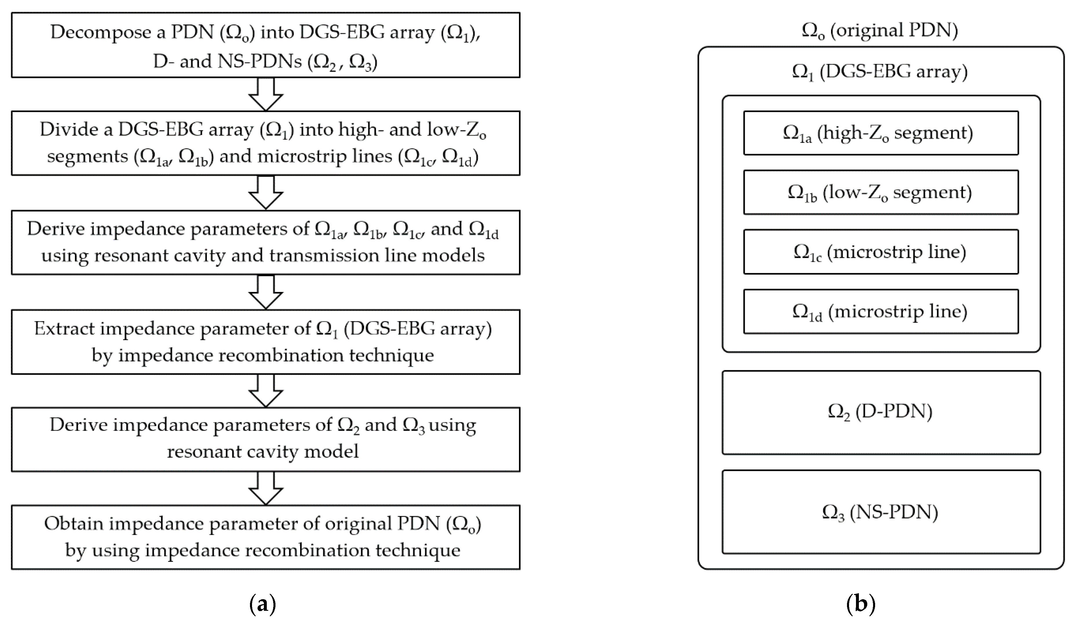
2.1. Overview of Proposed DDM
2.2. Segment Modeling
- (1)
- Constant factor
- (2)
- Green’s-function-like factor
- (3)
- Cosine factors
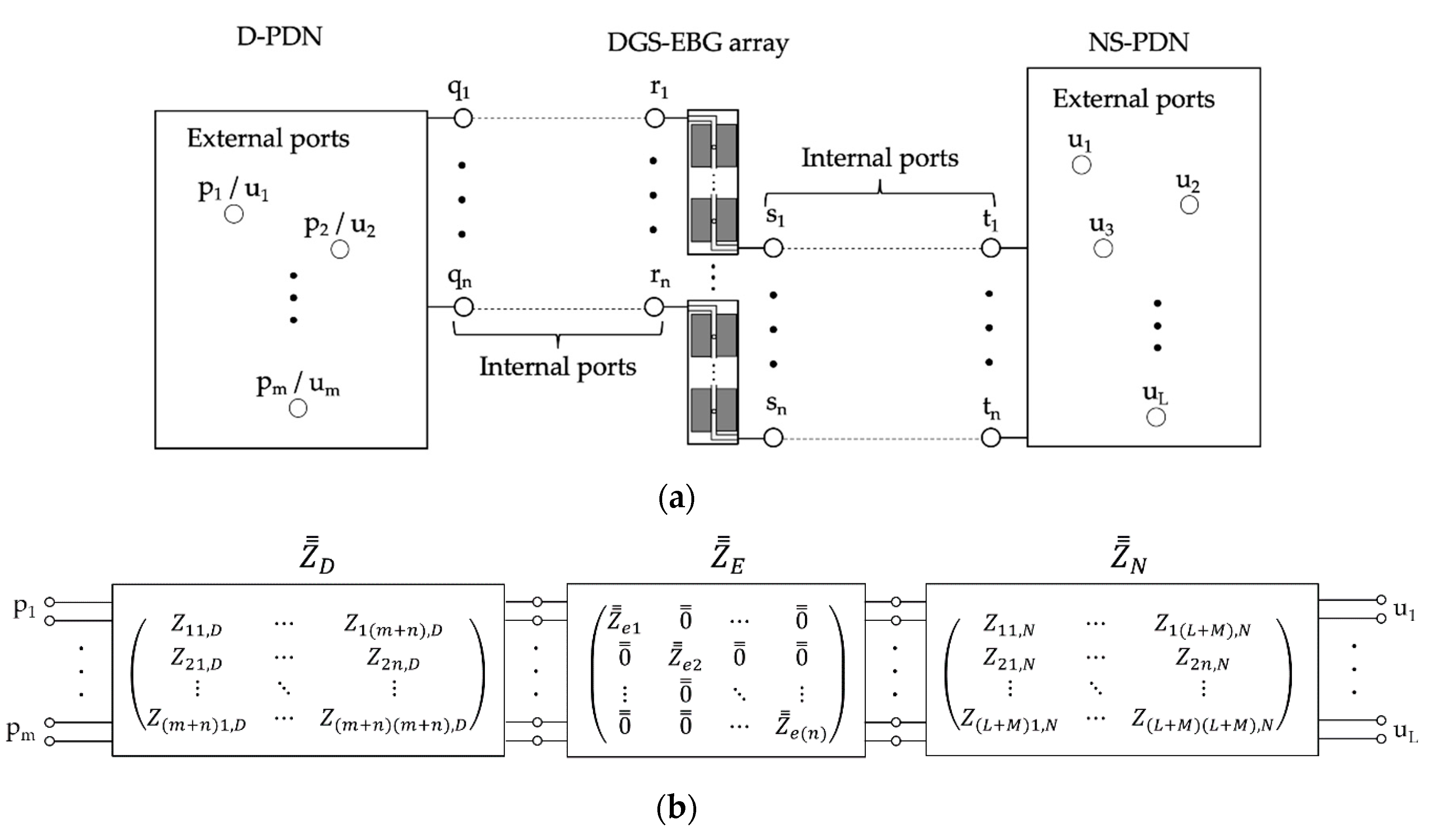
2.3. Recombination
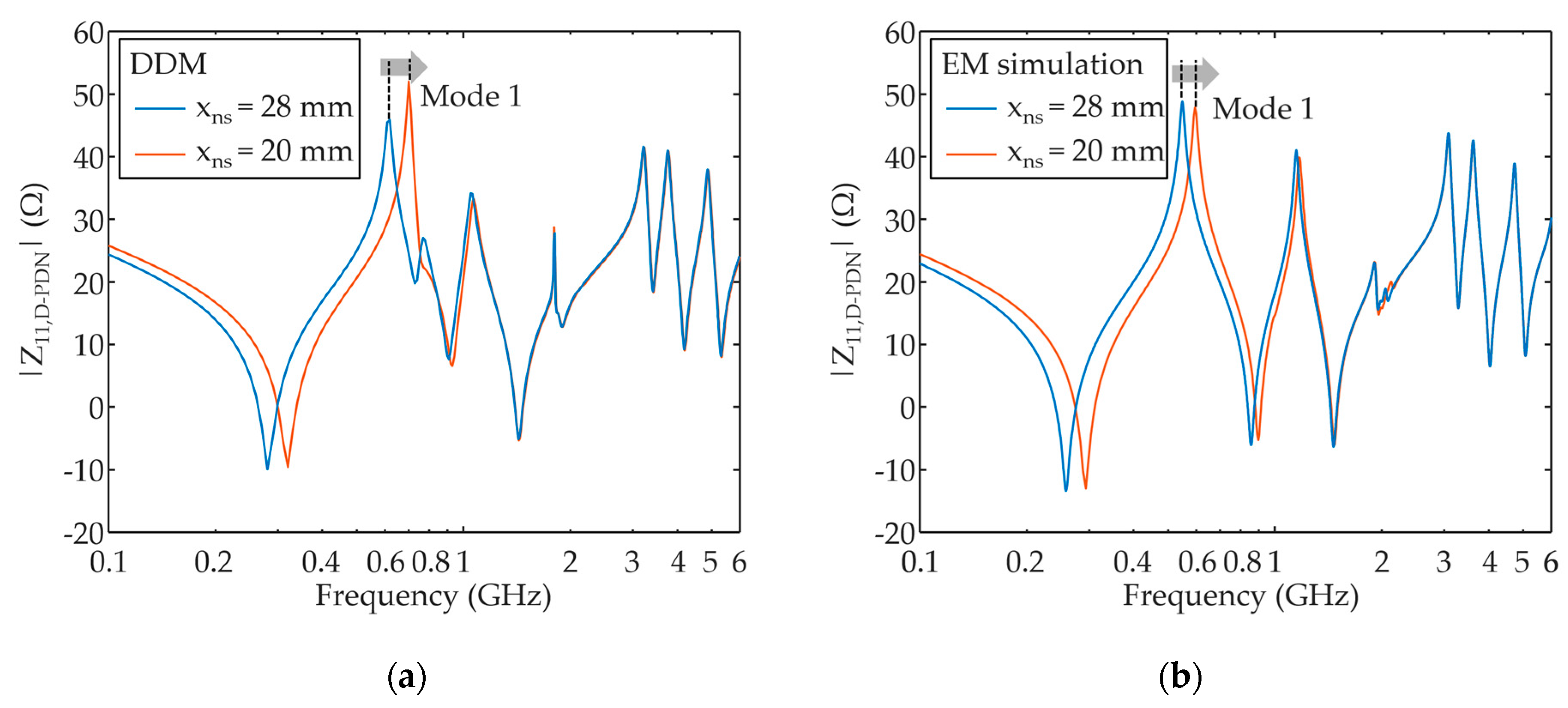
3. Results and Discussion
4. Conclusions
Funding
Conflicts of Interest
References
- McCredie, B.D.; Becker, W.D. Modeling, measurement, and simulation of simultaneous switching noise. IEEE Trans. Compon. Packag. Manuf. Technol. Part B 1996, 19, 461–472. [Google Scholar] [CrossRef]
- Chun, S.; Swaminathan, M.; Smith, L.D.; Srinivasan, J.; Jin, Z.; Iyer, M.K. Modeling of simultaneous switching noise in high speed systems. IEEE Trans. Adv. Packag. 2001, 24, 132–142. [Google Scholar] [CrossRef]
- Wu, T.-L.; Chuang, H.-H.; Wang, T.-K. Overview of power integrity solutions on package and PCB: Decoupling and EBG isolation. IEEE Trans. Electromagn. Compat. 2010, 52, 346–356. [Google Scholar] [CrossRef]
- Li, E.-P.; Wei, X.; Cangellaris, A.C.; Liu, E.-X.; Zhang, Y.; D’Amore, M.; Kim, J.; Sudo, T. Progress Review of Electromagnetic Compatibility Analysis Technologies for Packages, Printed Circuit Boards, and Novel Interconnects. IEEE Trans. Electromagn. Compat. 2010, 52, 248–265. [Google Scholar]
- Swaminathan, M.; Chung, D.; Grivet-Talocia, S.; Bharath, K.; Laddha, V.; Xie, J. Designing and Modeling for Power Integrity. IEEE Trans. Electromagn. Compat. 2010, 52, 288–310. [Google Scholar] [CrossRef]
- Chen, J.Y.; Jone, W.B.; Wang, J.S.; Lu, H.; Chen, T.F. Segmented bus design for low-power systems. IEEE Trans. Very Large Scale Integr. (VLSI) Syst. 1999, 7, 25–29. [Google Scholar] [CrossRef]
- Fan, J.; Drewniak, J.; Shi, H.; Knighten, J. DC power-bus modeling and design with a mixed-potential integral-equation formulation and circuit extraction. IEEE Trans. Electromagn. Compat. 2001, 43, 426–436. [Google Scholar] [CrossRef]
- Cui, W.; Fan, J.; Ren, Y.; Shi, H.; Drewniak, J.; Dubroff, R. DC power-bus noise isolation with power-plane segmentation. IEEE Trans. Electromagn. Compat. 2003, 45, 436–443. [Google Scholar] [CrossRef]
- Wang, Z.; Wada, O.; Toyota, Y.; Koga, R. Modeling of gapped power bus structures for isolation using cavity modes and segmentation. IEEE Trans. Electromagn. Compat. 2005, 47, 210–218. [Google Scholar] [CrossRef]
- Hampe, M.; Dickmann, S. Improving the behavior of PCB power-bus structures by an appropriate segmentation. In Proceedings of the 2005 International Symposium on Electromagnetic Compatibility (EMC 2005), Chicago, IL, USA, 8–12 August 2005; Volume 3, pp. 961–966. [Google Scholar]
- Feng, G.; Fan, J. Analysis of Simultaneous Switching Noise Coupling in Multilayer Power/Ground Planes With Segmentation Method and Cavity Model. IEEE Trans. Electromagn. Compat. 2010, 52, 699–711. [Google Scholar] [CrossRef]
- Feng, G.; Fan, J. An Extended Cavity Method to Analyze Slot Coupling Between Printed Circuit Board Cavities. IEEE Trans. Electromagn. Compat. 2010, 53, 140–149. [Google Scholar] [CrossRef]
- Preibisch, J.B.; Duan, X.; Schuster, C. An Efficient Analysis of Power/Ground Planes with Inhomogeneous Substrates Using the Contour Integral Method. IEEE Trans. Electromagn. Compat. 2013, 56, 980–989. [Google Scholar] [CrossRef]
- Shi, L.-F.; Sun, Z.-M.; Liu, G.-X.; Chen, S. Hybrid-Embedded EBG Structure for Ultrawideband Suppression of SSN. IEEE Trans. Electromagn. Compat. 2017, 60, 747–753. [Google Scholar] [CrossRef]
- De Paulis, F.; Nisanci, M.H.; Orlandi, A. Practical EBG application to multilayer PCB: Impact on power integrity. IEEE Electromagn. Compat. Mag. 2012, 1, 60–65. [Google Scholar] [CrossRef]
- Zhu, H.-R.; Sun, Y.-F.; Huang, Z.; Wu, X.-L. A Compact EBG Structure with Etching Spiral Slots for Ultrawideband Simultaneous Switching Noise Mitigation in Mixed Signal Systems. IEEE Trans. Compon. Packag. Manuf. Technol. 2019, 9, 1559–1567. [Google Scholar] [CrossRef]
- Shi, L.-F.; Zhang, G.; Jin, M.-M.; Chen, S.; Hu, X.-J. Novel Subregional Embedded Electromagnetic Bandgap Structure for SSN Suppression. IEEE Trans. Compon. Packag. Manuf. Technol. 2016, 6, 613–621. [Google Scholar] [CrossRef]
- Wu, T.-L.; Fan, J.; De Paulis, F.; Wang, C.-D.; Scogna, A.C.; Orlandi, A. Mitigation of noise coupling in multilayer high-speed PCB: State of the art modeling methodology and EBG technology. IEICE Trans. Commun. 2010, E93-B, 1678–1689. [Google Scholar] [CrossRef]
- Kim, M.; Koo, K.; Kim, J. Noise isolation modeling of partial EBG power bus using segmentation method and cavity model in multi-layer PCBs. In Proceedings of the 2011 IEEE International Symposium on Electromagnetic Compatibility, Long Beach, CA, USA, 14–19 August 2011; pp. 710–714. [Google Scholar]
- Wang, T.-H.; Chiang, J.-W.; Lin, D.-B. Combine partial EBG structure and Z-shape power bus for noise isolation in multi-layer PCBs. In Proceedings of the 2015 Asia-Pacific Symposium on Electromagnetic Compatibility (APEMC), Taipei, Taiwan, 26–29 May 2015; pp. 106–108. [Google Scholar]
- Kim, M.; Kam, D.G. Wideband and Compact EBG Structure With Balanced Slots. IEEE Trans. Compon. Packag. Manuf. Technol. 2015, 5, 818–827. [Google Scholar] [CrossRef]
- Wang, T.-H.; Zheng, L.-Z.; Lin, D.-B.; Hsieh, M.-H. On the simultaneous switching noise suppression by the integration of Z-shape power bus and bandstop filter. In Proceedings of the 2018 IEEE International Symposium on Electromagnetic Compatibility and 2018 IEEE Asia-Pacific Symposium on Electromagnetic Compatibility (EMC/APEMC), Singapore, 14–18 May 2018; pp. 973–976. [Google Scholar]
- Lin, D.-B.; Wang, T.-H.; Chiang, J.-W. Suppression of Wideband Simultaneous Switching Noise Through Application of a Partial Electromagnetic Band-Gap Structure in Multilayer Printed Circuit Boards. IEEE Trans. Electromagn. Compat. 2020, 62, 1247–1255. [Google Scholar] [CrossRef]
- Zhang, M.-S.; Tan, H.Z. IR-drop modeling and reduction for high-performance printed circuit boards. IEEE Electromagn. Compat. Mag. 2015, 4, 90–101. [Google Scholar] [CrossRef]
- Kim, J.; Wu, S.; Wang, H.; Takita, Y.; Takeuchi, H.; Araki, K.; Feng, G.; Fan, J. Improved target impedance and IC transient current measurement for power distribution network design. In Proceedings of the 2010 IEEE International Symposium on Electromagnetic Compatibility, Fort Lauderdale, FL, USA, 25–30 July 2010; pp. 445–450. [Google Scholar]
- Zhang, N.M.-S.; Tan, N.H.-Z.; Mao, N.J.-F. New Power Distribution Network Design Method for Digital Systems Using Time-Domain Transient Impedance. IEEE Trans. Compon. Packag. Manuf. Technol. 2013, 3, 1399–1408. [Google Scholar] [CrossRef]
- Kim, J.; Takita, Y.; Araki, K.; Fan, J. Improved Target Impedance for Power Distribution Network Design With Power Traces Based on Rigorous Transient Analysis in a Handheld Device. IEEE Trans. Compon. Packag. Manuf. Technol. 2013, 3, 1554–1563. [Google Scholar]
- Kim, Y.; Kim, K.; Cho, J.; Kim, J.; Kang, K.; Yang, T.; Ra, Y.; Paik, W. Power distribution network design and optimization based on frequency dependent target impedance. In Proceedings of the 2015 IEEE Electrical Design of Advanced Packaging and Systems Symposium (EDAPS), Seoul, Korea, 14–16 December 2015; pp. 89–92. [Google Scholar]
- Smith, L.; Anderson, R.; Forehand, D.; Pelc, T.; Roy, T. Power distribution system design methodology and capacitor selection for modern CMOS technology. Advanced Packaging. IEEE Trans. Adv. Packag. 1999, 22, 284–291. [Google Scholar] [CrossRef]
- Kim, H.; Sun, B.K.; Kim, J. Suppression of GHz range power/ground inductive impedance and simultaneous switching noise using embedded film capacitors in multilayer packages and PCBs. IEEE Microw. Wirel. Compon. Lett. 2004, 14, 71–73. [Google Scholar]
- Engin, A.E. Efficient Sensitivity Calculations for Optimization of Power Delivery Network Impedance. IEEE Trans. Electromagn. Compat. 2010, 52, 332–339. [Google Scholar] [CrossRef][Green Version]
- Luo, G.-X.; Cui, X.; Wei, X.-C.; Li, E.-P. Distributed decoupling analysis on PG planes for PDN design. In Proceedings of the International Symposium on Electromagnetic Compatibility-EMC EUROPE, Rome, Italy, 17–21 September 2012; pp. 1–5. [Google Scholar]
- Chen, J.; Hashimoto, M. A Frequency-Dependent Target Impedance Method Fulfilling Voltage Drop Constraints in Multiple Frequency Ranges. IEEE Trans. Compon. Packag. Manuf. Technol. 2020, 10, 1769–1781. [Google Scholar] [CrossRef]
- Kim, B.; Kim, D.-W. Improvement of Simultaneous Switching Noise Suppression of Power Plane using Localized Spiral-Shaped EBG Structure and λ/4 Open Stubs. In Proceedings of the 2007 Asia-Pacific Microwave Conference, Bangkok, Thailand, 11–14 December 2007; pp. 1–4. [Google Scholar]
- Zhu, H.-R.; Mao, J.-F. Localized Planar EBG Structure of CSRR for Ultrawideband SSN Mitigation and Signal Integrity Improvement in Mixed-Signal Systems. IEEE Trans. Compon. Packag. Manuf. Technol. 2013, 3, 2092–2100. [Google Scholar] [CrossRef]
- Engin, A.E.; Ndip, I.; Lang, K.-D.; Aguirre, G. Power Plane Filter Using Higher Order Virtual Ground Fence. IEEE Trans. Compon. Packag. Manuf. Technol. 2017, 7, 519–525. [Google Scholar] [CrossRef]
- Ludwig, R. RF Circuit Design Theory and Applications; Prentice-Hall: Englewood Cliffs, NJ, USA, 2000. [Google Scholar]
- Lei, G.-T.; Techentin, R.; Gilbert, B. High-frequency characterization of power/ground-plane structures. IEEE Trans. Microw. Theory Tech. 1999, 47, 562–569. [Google Scholar]
- Okoshi, T. Planar Circuits for Microwave and Lightwaves; Springer: New York, NY, USA, 1985; pp. 85–96. [Google Scholar]
- Ansys. Ansys SIwave. Available online: https://www.ansys.com/products/electronics/ansys-siwave (accessed on 23 November 2020).
- Kim, M.; Koo, K.; Hwang, C.; Shim, Y.; Kim, J.; Kim, J. A Compact and Wideband Electromagnetic Bandgap Structure Using a Defected Ground Structure for Power/Ground Noise Suppression in Multilayer Packages and PCBs. IEEE Trans. Electromagn. Compat. 2012, 54, 689–695. [Google Scholar]


| Parameters | Dimensions | Parameters | Dimensions |
|---|---|---|---|
| xd | 20 | hHS | 0.8 |
| yd | 23 | hLS | 0.1 |
| xns | 28 | (xp1, yp1) | (5, 4) |
| yns | 36 | (xq1, yq1) | (20, 22) |
| dc | 4 | (xq2, yq2) | (20, 10.9) |
| dp | 3.8 | (xr1, yr1) | (24, 12) |
| ddgs | 3.4 | (xr2, yr2) | (24, 0.9) |
Publisher’s Note: MDPI stays neutral with regard to jurisdictional claims in published maps and institutional affiliations. |
© 2020 by the author. Licensee MDPI, Basel, Switzerland. This article is an open access article distributed under the terms and conditions of the Creative Commons Attribution (CC BY) license (http://creativecommons.org/licenses/by/4.0/).
Share and Cite
Kim, M. Power Integrity Analysis of Power Distribution Network Segmented Using DGS–Electromagnetic Bandgap Structure in Mixed-Signal PCBs. Electronics 2020, 9, 2036. https://doi.org/10.3390/electronics9122036
Kim M. Power Integrity Analysis of Power Distribution Network Segmented Using DGS–Electromagnetic Bandgap Structure in Mixed-Signal PCBs. Electronics. 2020; 9(12):2036. https://doi.org/10.3390/electronics9122036
Chicago/Turabian StyleKim, Myunghoi. 2020. "Power Integrity Analysis of Power Distribution Network Segmented Using DGS–Electromagnetic Bandgap Structure in Mixed-Signal PCBs" Electronics 9, no. 12: 2036. https://doi.org/10.3390/electronics9122036
APA StyleKim, M. (2020). Power Integrity Analysis of Power Distribution Network Segmented Using DGS–Electromagnetic Bandgap Structure in Mixed-Signal PCBs. Electronics, 9(12), 2036. https://doi.org/10.3390/electronics9122036