Article

A Novel Highly Linear Voltage-To-Time Converter (VTC) Circuit for Time-Based Analog-To-Digital Converters (ADC) Using Body Biasing

1
Department of Electrical Engineering, Port-Said University, Port-Said 42526, Egypt
2
Department of Electronics and Communications Engineering, Cairo University, Giza 12613, Egypt
3
Nanotechnology and Nanoelectronics Program, University of Science and Technology, Zewail City of Science and Technology, October Gardens, 6th of October, Giza 12578, Egypt
4
Department of Communication and Electronics, Faculty of Engineering, Menoufia University, Menouf 32952, Egypt
*
Author to whom correspondence should be addressed.
Electronics 2020, 9(12), 2033; https://doi.org/10.3390/electronics9122033
Submission received: 10 October 2020 / Revised: 26 November 2020 / Accepted: 28 November 2020 / Published: 1 December 2020
(This article belongs to the Section Microelectronics)

Abstract

:
Time-based analog-to-digital converter is considered a crucial part in the design of software-defined radio receivers for its higher performance than other analog-to-digital converters in terms of operation speed, input dynamic range and power consumption. In this paper, two novel voltage-to-time converters are proposed at which the input voltage signal is connected to the body terminal of the starving transistor rather than its gate terminal. These novel converters exhibit better linearity, which is analytically proven in this paper. The maximum linearity error is reduced to 0.4%. In addition, the input dynamic range of these converters is increased to 800 mV for a supply voltage of 1.2 V by using industrial hardware-calibrated TSMC 65 nm CMOS technology. These novel designs consist of only a single inverter stage, which results in reducing the layout area and the power consumption. The overall power consumption is 18 μW for the first proposed circuit and 15 μW for the second proposed circuit. The novel converter circuits have a resolution of 5 bits and operate at a maximum clock frequency of 500 MHz.

1. Introduction

Analog-to-digital converter (ADC) is considered the link between the real world, represented by real-time analog signals (speech, radar, medical imaging, etc.), and the digitized world, represented by digital integrated circuits, microprocessors and microcontrollers. ADCs are the key components in most recent electronic devices especially in software-defined radio (SDR), biomedical devices and low-power electronic devices.
Recent ADC architectures are facing many serious limitations due to CMOS technology scaling [1]. One of these limitations is the degradation of the signal-to-noise ratio (SNR) due to the reduction of the supply voltage. Moreover, the dynamic range of analog input signal is reduced as the threshold voltage is not affected by the continuous scaling of CMOS transistors.
These limitations led to the design of the time-based analog-to-digital converter (T-ADC). In this ADC, the input voltage signal is converted to a delay signal first where the delay is proportional to the input signal value. Following that, this delay signal is converted to a digital code. This allows the processing of the signal to be in the time domain [2]. This is an important advantage because time resolution has been improved in nanometer-scale devices due to the reduction of gate delay, despite the reduction in supply voltage.
The T-ADC consists of two stages, as shown in Figure 1a. The first stage is a voltage-to-time converter (VTC) that converts the input signal to delay pulses. The delay in each pulse is proportional to the value of the input voltage signal. The second stage is a time-to-digital converter (TDC) that converts these delay pulses to a digital code [3].
The most commonly used VTC circuit is the simple current starving inverter shown in Figure 1b. It consists of a CMOS inverter with an NMOS starving transistor connected in the driver branch [3]. The input voltage, which is connected to the gate of the starving NMOS transistor, controls the current of the driver branch when the output of the inverter goes from ‘1’ to ‘0’. In other words, the fall time of the output voltage of the inverter is directly proportional to the input voltage signal.
The performance of the VTC circuit is limited by two major drawbacks. These drawbacks are the output delay non-linearity and the limited dynamic range of the input signal. One of the main challenges in the design of the VTC circuit is the non-linearity that appears in the fall time of the output response for high input values. In other words, when the input voltage increases, the delay curves for the output exhibit much non-linearity, which results in inaccurate conversion of the input signal to digital code.
This non-linearity happens because during the fall time of the output signal, the starving transistor is operating in saturation mode with a current of:
I D =   K 2 × W L   ( V GS   V T ) 2
where k’ is a constant, W/L is the aspect ratio of the transistor, VGS is the gate-to-source voltage, which is connected to the input signal, and VT is the threshold voltage of the starving transistor. The fall-time output delay is determined as follows:
I D = C   dV dt ,   dt = C   dV I D  
where C is the parasitic capacitance at the output, dV is the voltage change at the output during discharging from ‘1′ to ‘0′ and dt is the fall-time output delay.
From the two previous equations, it is obvious that the relation between the input voltage and the output delay time is non-linear, and this non-linearity increases by increasing the input voltage.
Limited dynamic range is also considered a major problem in the design of the VTC circuit. The input signal should not have small values because it is connected to the gate of the starving NMOS transistor. Thus, its value must be greater than the threshold voltage of the transistor to turn it on and create a path for the output to ground.
Many modified VTC circuits have been proposed by researchers [3,4,5,6,7,8,9,10,11,12] to overcome the previously mentioned drawbacks of the conventional VTC circuit. However, these circuits are not sufficiently linear and have low resolution. In Reference [3], a linearization scheme has been proposed achieving a maximum linearity error of 2%. However, the input dynamic range is only 200 mV. In Reference [4], a VTC circuit is proposed to operate at 5 GS/s. However, the circuit consumes high power of 3.6 mW and has a small input dynamic range of 100 mV. In Reference [5], the authors have modified the VTC circuit in Reference [4] to increase the input dynamic range to 140 mV. In Reference [6], a VTC circuit is proposed at which the input signal is compared with a voltage ramp. Although this design in Reference [6] consumes low power, it operates at a small sampling frequency of 1 MHz. In Reference [7], a differential VTC circuit is proposed to achieve a maximum linearity error of 3% at a very small input dynamic range of 172 mV.
In Reference [8], a VTC is proposed that consists of a track and hold circuit, level shifter and a pulse shape restorer which improves the linearity of the VTC. However, this design does not offer sufficient linearity and suffers from high power consumption. A VTC with a two-step transition inverter delay line is proposed in Reference [9]. However, this design has low sensitivity of 0.1 ps/mV and consumes relatively high power of 180 μW.
In Reference [10], a current-to-time converter (CDC) based on the conventional starved inverter is introduced. However, the maximum linearity error is 2.1% and the modified circuit operates at a low clock frequency of 50 MHz. In Reference [11], a modified VTC is introduced to increase the linearity but the power consumption of this design is high (3.35 mW), and the input dynamic range is limited to 400 mV. In Reference [12], a fully digital time-based ADC is proposed to reduce the chip area at which the power consumption is reduced to 380 μW but still relatively high.
Another promising approach is using Voltage-Controlled Oscillators (VCO) instead of the VTC at which the frequency of the VCO is proportional to the input voltage signal [13]. VCO-based ADCs are all-digital ADCs that operate at low power consumption levels and consume lower chip areas. However, VCO-based ADCs have a significant drawback which is the non-linearity of the VCO. Moreover, VCOs are sensitive to process, voltage and temperature (PVT) variations [14].
In Reference [13], an all-digital VCO-based ADC is proposed at which a digital linearization block is implemented. This linearization block uses polynomial-fit non-linearity estimation to suppress the non-linearity. However, this design consumes a relatively high power of 3.3 mW. In Reference [14], a second-order, VCO-based continuous-time (CT) ADC is proposed at which two VCOs are used as integrators to realize second-order quantization noise shaping. However, this design consumes high chip area (0.06 mm2) and high power (1 mW). In Reference [15], a Nyquist-rate fully synthesizable Successive Approximation Register (SAR) voltage-input ADC is proposed which is based on the Dyadic Digital Pulse Modulation (DDPM). This design has a great advantage of exhibiting very low chip area (0.003 mm2) and very small power consumption (3.1 μW). However, the sampling frequency is very low (2.8 kS/s). In Reference [16], a VCO-based non-uniform sampling (NUS) analog-to-digital converter (ADC) is proposed. In this design, there is no need for any continuous-time (CT) comparator or reference generator as the proposed ADC shifts the conventional voltage-domain level crossing to the phase domain. This proposed ADC operates at high sampling frequency of 4 GHz. However, the power consumption is high (49.7 mW), and the chip area used is also high (0.244 m2). In Reference [17], a voltage-to-frequency converter (VFC) is proposed to achieve a maximum linearity error of 3%. However, this design provides a small input dynamic range of 320 mV.
In this paper, two novel VTC circuits are proposed based on the body biasing technique, where the input signal is connected to the body terminal of the starving transistor rather than its gate terminal. The proposed VTC circuits achieve highly linear output delay response with a wide input dynamic range of 800 mV and a maximum linearity error of 0.55% for the first proposed VTC and 0.4% for the second proposed VTC.
The rest of the paper is organized as follows. Section 2 describes the proposed VTC circuits design and analysis in details. The simulation results are presented in Section 3, followed by a discussion on the important factors that affect the performance of the proposed VTC circuit in Section 4. Finally, the conclusions are stated in Section 5.

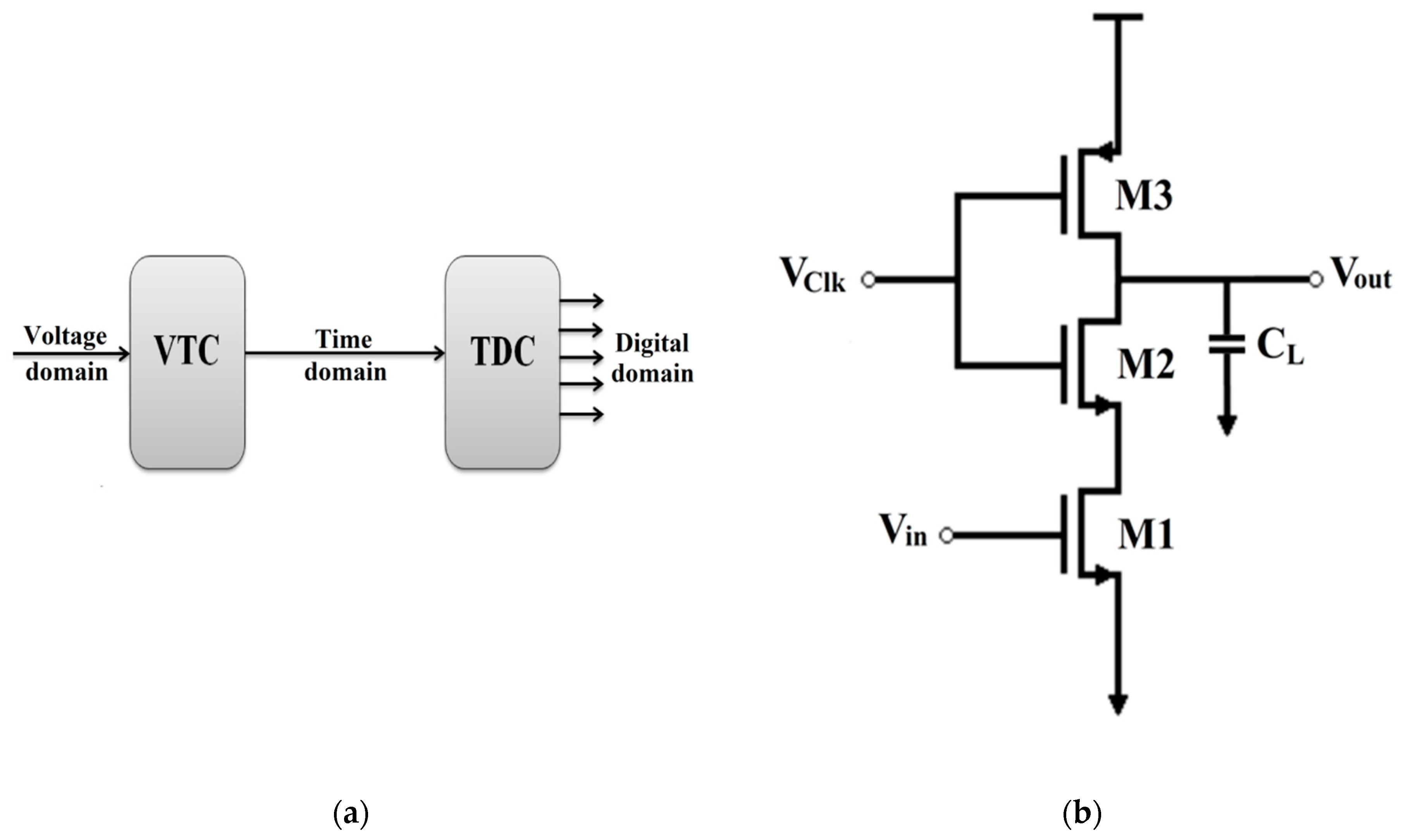
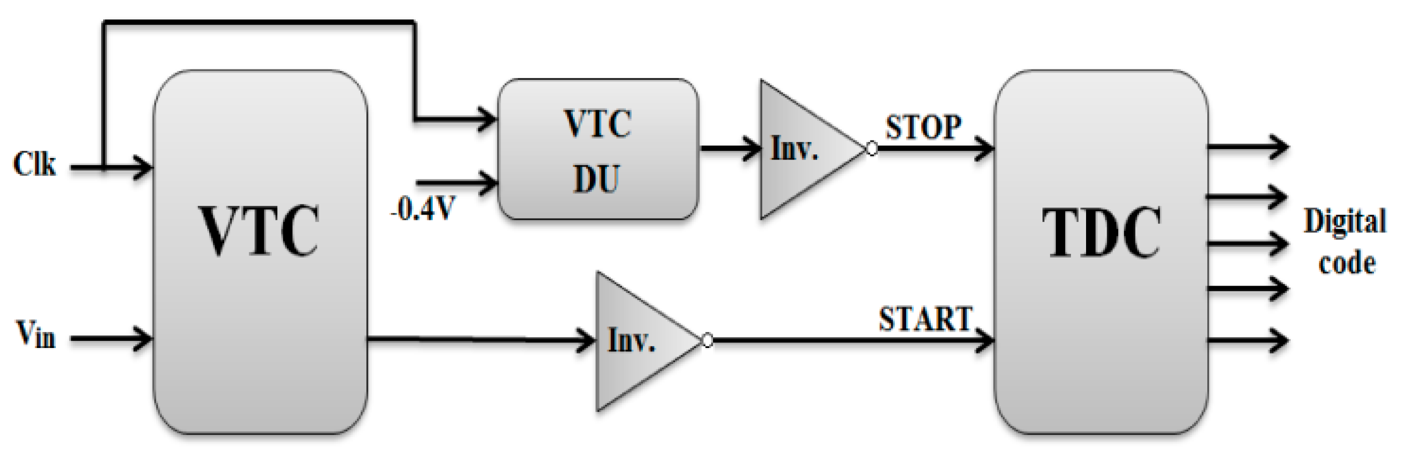
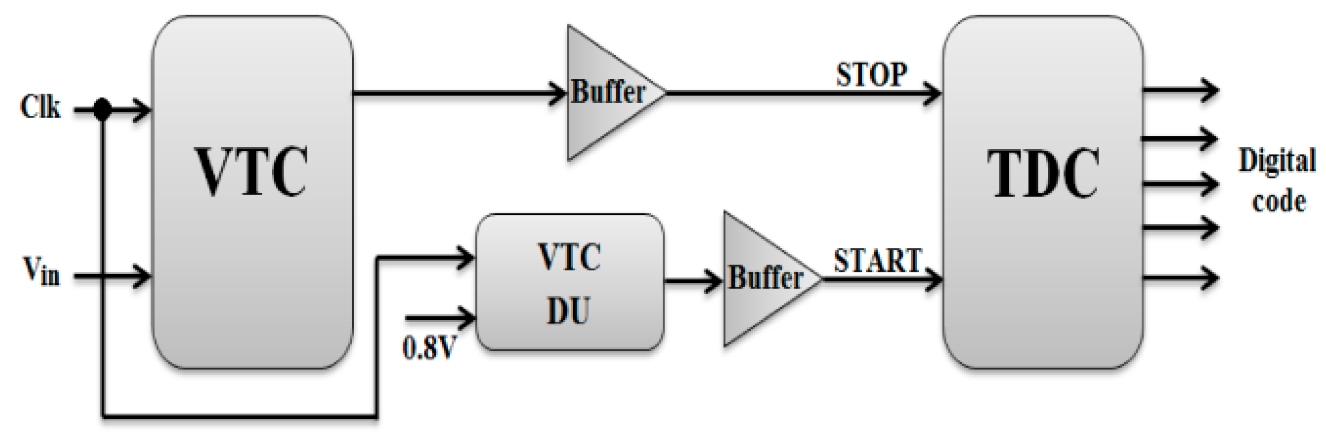
2. Proposed Circuits Design and Analysis

The theory of operation for the proposed circuits is based on the body biasing technique at which the input signal is connected to the body terminal of the starving transistor. The body biasing technique results in a highly linear drain current with respect to the body-to-source voltage of the starving transistors, as proven below.
The body biasing technique can be applied on a falling-time starving inverter at which the starving transistor is NMOS. In addition, it can be applied on a rise-time starving inverter at which the starving transistor is PMOS. Both cases are discussed below in detail.

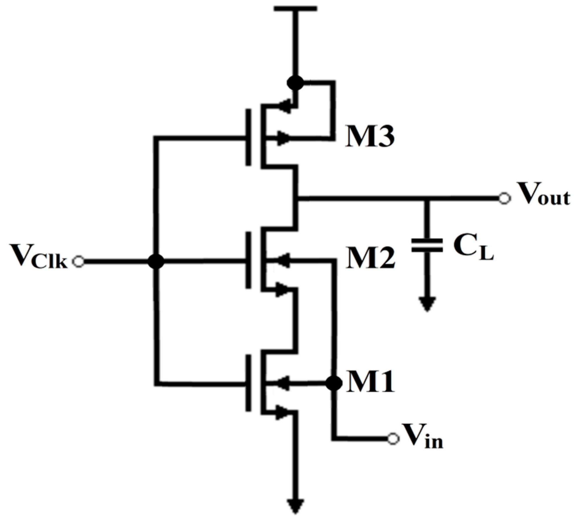
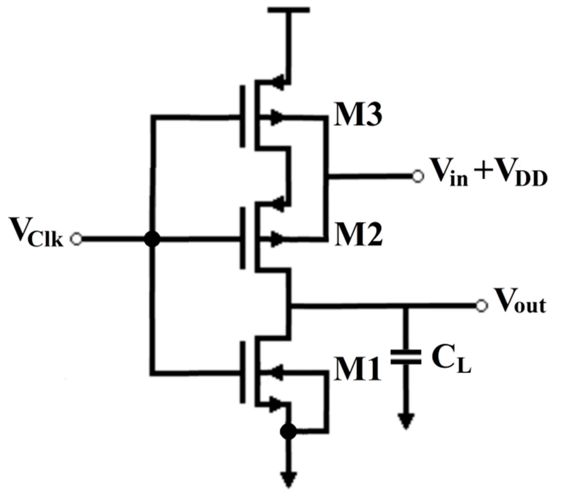
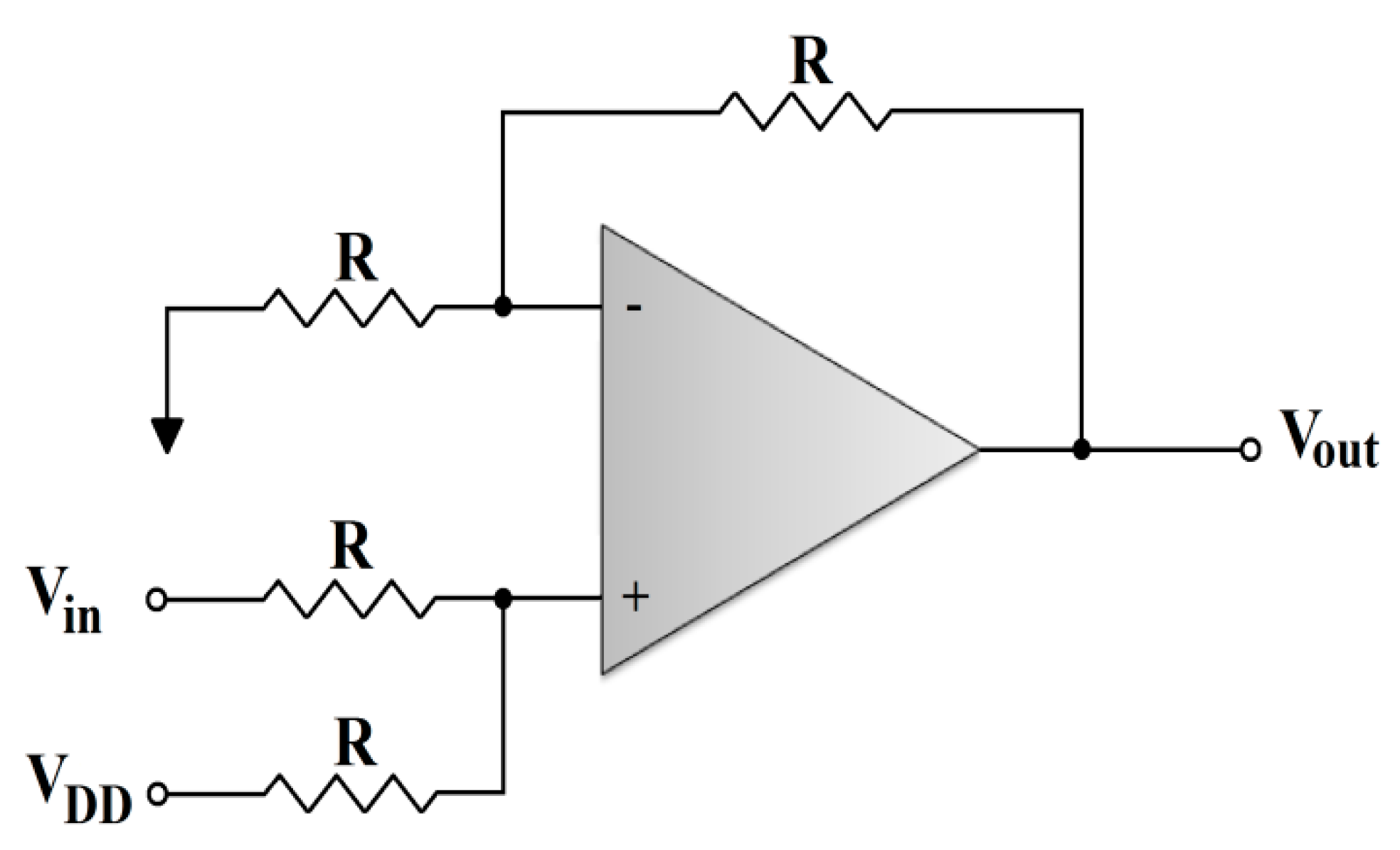
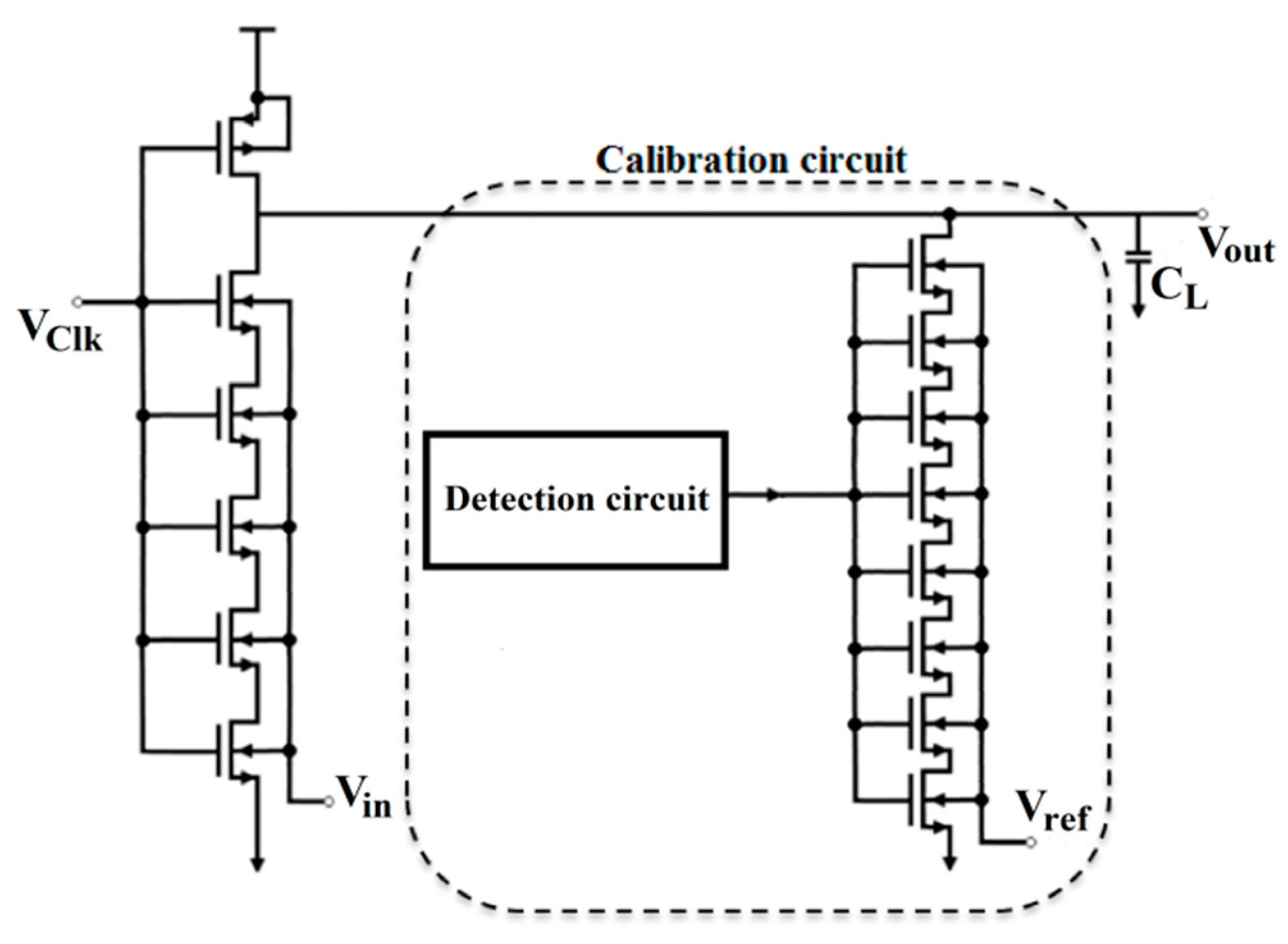
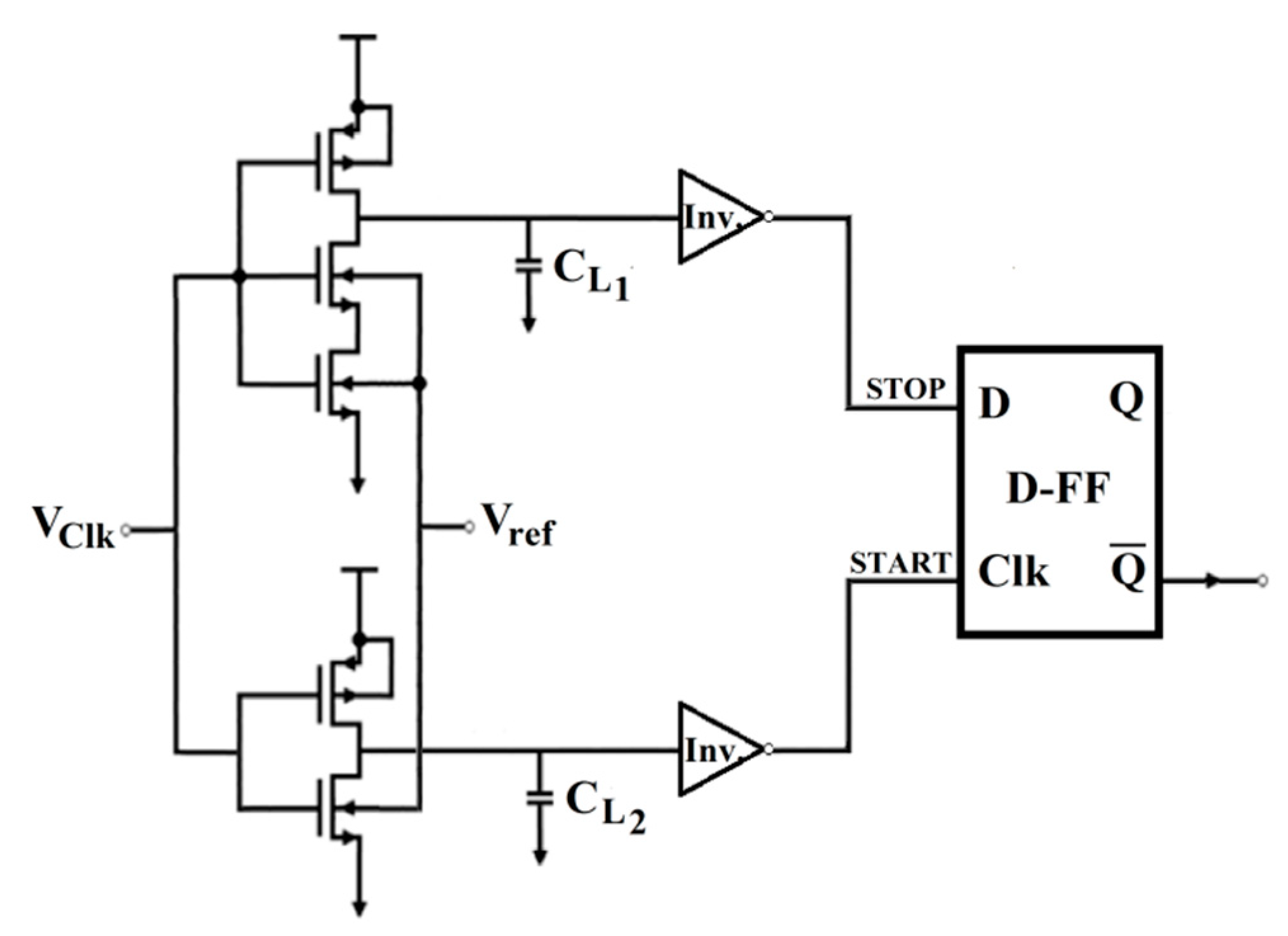
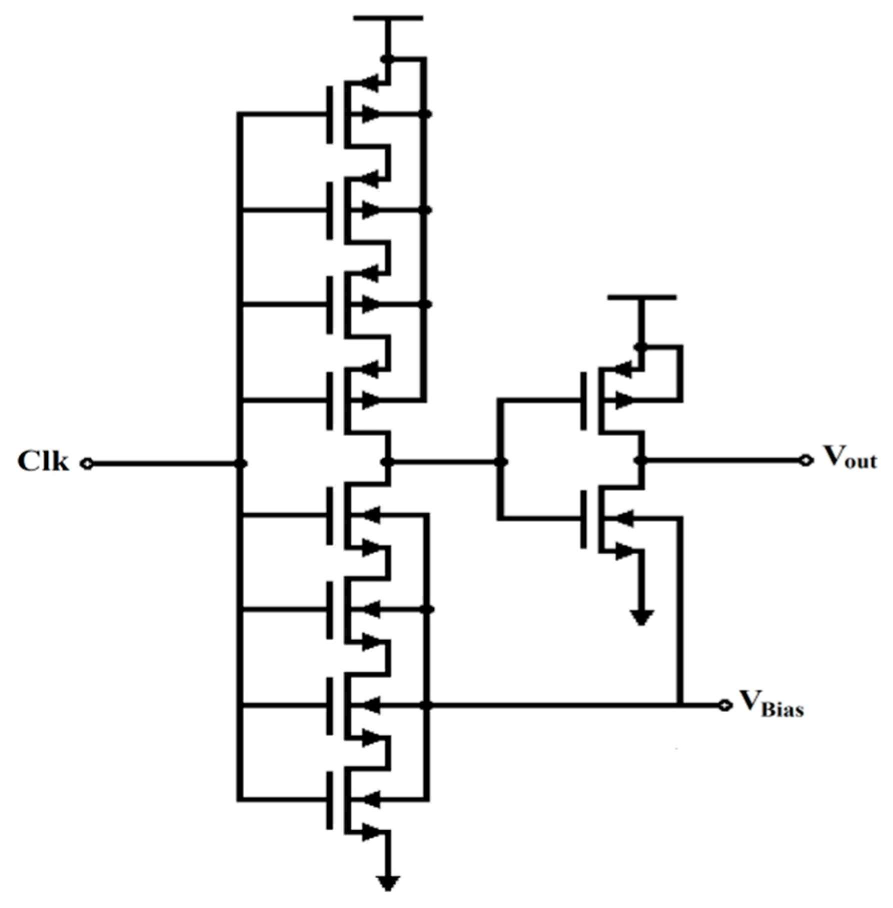
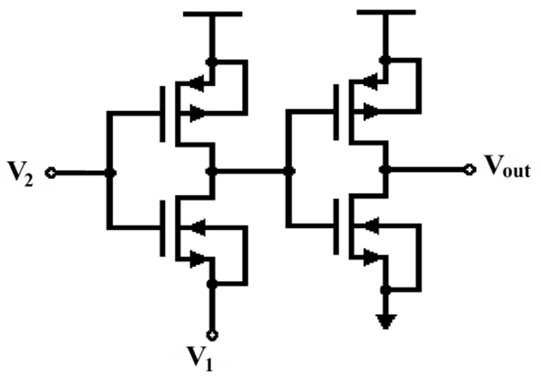
2.1. First Proposed VTC

The proposed circuit is introduced as shown in Figure 2. The input signal is applied to the body terminal of the NMOS starving transistor. The output load capacitance CL equals to 30 fF (for FO4).
In this VTC, the threshold voltage of the starving transistor, VT, is a function of the body-to-source voltage (which represents the input signal) and is given by:
V T =   V T o + γ ( | 2 f V B S | | 2 f | )    
where VTO is the zero-bias threshold voltage, γ is the body effect factor, VBS is the body-to-source voltage and f is the Fermi potential.
The following analytical proof shows that the body biasing provides a linear relation between the drain current of the starving transistor (which represents the discharging current of the output load capacitance) and the body-to-source voltage. The proof is derived as follows:
  I D = K n 2   ( V G S V T ) 2
    I D = K n 2 ( V G S 2 2 V G S V T + V T 2 )
V T =   V T o γ | 2 f |   + γ | 2 f V B S |
V T =   V T o γ | 2 f |   + γ | 2 f |   | 1 V B S 2 f |
  1 + x   1 +   x 2 ,     f o r   x < 1         ( T a y l o r   s e r i e s   e x p a n s i o n )
V T =   V T O γ | 2 f | + γ | 2 f |   ( 1 V B S 2 | 2 f | )
V T =   V T O γ | 2 f |   ( V B S 2 | 2 f | )
V T =   V T O ( γ 2 | 2 f |   ) V B S    
V T 2   V T O 2 ( V T O γ | 2 f |   ) V B S
Substitute (11) and (12) into (5):
  I D     K 1 + K 2   V B S
where,
K 1 = K n 2   ( V G S V T O ) 2
K 2 = K n γ 2 | 2 f | ( V G S V T O )
From (13) and (2):
d t =   C   d V K 1 +   K 2 V B S
Multiplying both numerator and denominator by the factor (k1k2.VBS), the fall time delay will be equal to:
d t =   K 1 C   d V K 1 2 K 2 2 V B S 2   K 2 C   d V   V B S K 1 2 K 2 2 V B S 2
Since VBS is dominant over VBS2 for values below 1, it is clear that the fall time delay (discharging time) of the output signal is linearly proportional to the input signal voltage which is applied to the body terminal.
Adding more series-identical NMOS transistors to the starving transistor helps in improving the performance of the circuit in two ways. First, the overall (W/L) of the series NMOS transistors is decreased as follows:
( W L ) t o t a l = ( W L ) / N
where N is the number of NMOS series transistors. This results in decreasing the discharge current which means that the delay time for the fixed voltage step of the input signal increases. Hence, the resolution of the proposed VTC circuit increases. Second, adding more series NMOS transistors decreases the gate-to-source voltage of the driver transistor M1. This guarantees that the driving transistor is kept in saturation to maintain linearity during all the discharging period of the output load capacitor.
Figure 3a shows the output delay of the proposed VTC circuit versus the number of series starving transistors (N). It is obvious that when the number of series starving transistors increases, the output delay range increases and the sensitivity (the rate of change of the output delay with respect to the input voltage) increases as well. The number of series starving transistors cannot exceed six for a clock frequency of 500 MHz as the output voltage will not have enough time to go logic ‘0′. For more series starving transistors, the clock frequency should be reduced for proper operation.
Figure 3b shows the sensitivity of the proposed VTC circuit versus the number of series starving transistors (N). For N having the values of four, five and six, the resolution of the proposed VTC will be 5 bits (for a least significant bit (LSB) of 5 ps). Four starving transistors are used for the final architecture of the proposed VTC circuit as it has a lower quantization error than having more starving transistors. Figure 4 shows the final architecture of the proposed VTC circuit.
The Forward Body Bias (FBB) voltage is limited by the forward biasing of the drain-bulk junction (the positive bound of the input voltage connected to the p-Well in case of NMOS and the negative bound of it below the supply voltage connected to the n-Well in case of PMOS). The FBB is also limited by the sub-threshold leakage current [18]. Moreover, the Reverse Body Bias (RBB) voltage bound is determined by the junction leakage current. In case of NMOS, the RBB voltage bound is the negative bound of the input voltage, connected to the p-Well, and the positive bound of over the supply voltage, connected to the n-Well in case of PMOS [18].
The upper limit of the FBB voltage is 0.6 V for latch-up free operation in 65 nm CMOS technology with a supply voltage that ranges from 0.9 to 1.2 V [18,19,20]. SPICE simulations are done by sweeping the FBB voltage of the PMOS transistor. These simulations show that the upper limit of the FBB voltage equals 0.59 V in order to prevent latch-up triggering for the NMOS transistor. Thus, the maximum FBB voltage is chosen to be equal to 0.4 V to avoid latch-up in case of FBB voltage fluctuations around 0.4 V. Moreover, the RBB voltage is also selected to be equal to 0.4 V. Hence, the FBB and the RBB maximum body voltages are chosen to be equal to ±0.4 V for NMOS devices and 1.2 ± 0.4 V for PMOS devices [18,21].
Thus, the input signal range is taken form −0.4 to 0.4 V, resulting in a full range of 800 mV. The maximum value of the input signal is 0.4 V to avoid latching up [18,21,22]. In other words, a short circuit path occurs between the supply voltage and ground when the body-to-source voltage exceeds 0.4 V in BULK-CMOS technology. This leads to a high current to pass, which results from parasitic bipolar devices in the CMOS circuits.
Latch-up can be avoided during the fabrication process by isolating NMOS and PMOS devices using an oxide trench along with a buried oxide layer. In addition, it can be avoided by increasing the spacing between CMOS devices, although this reduces packing density.

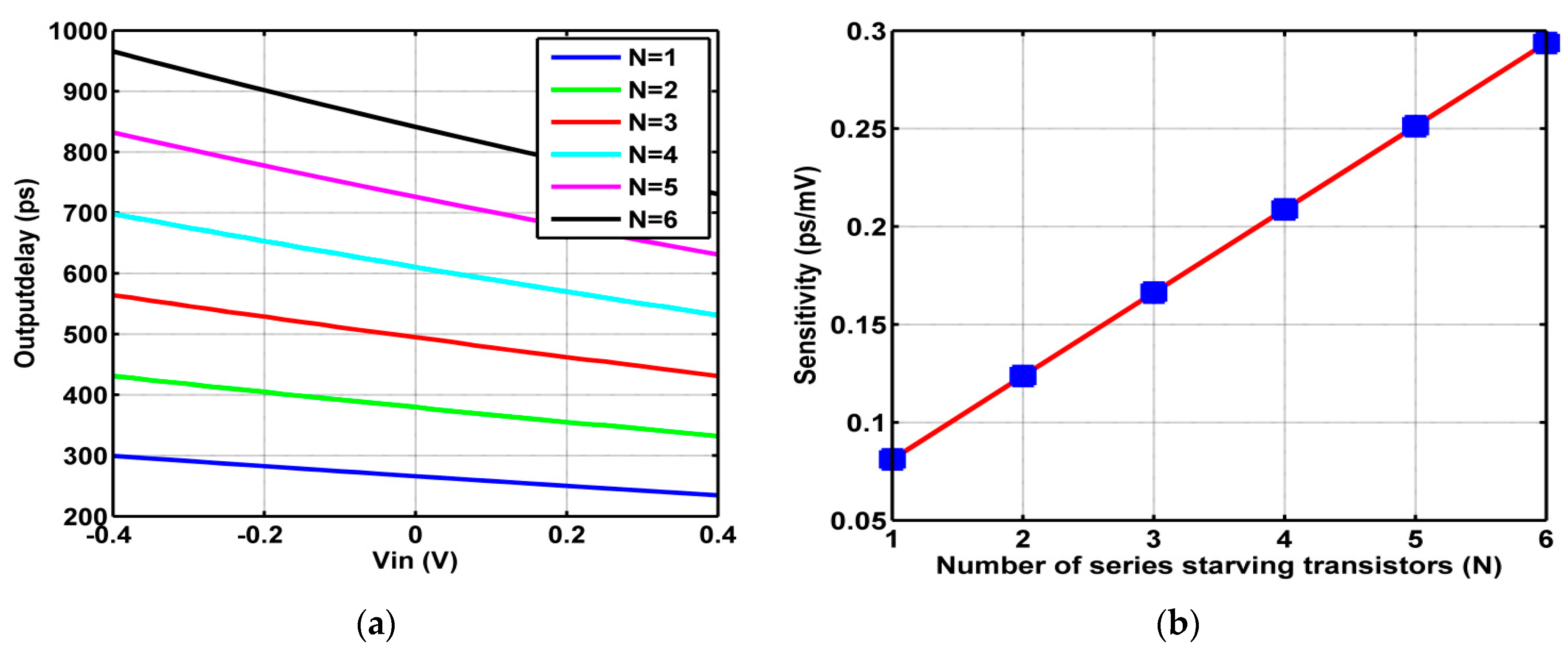
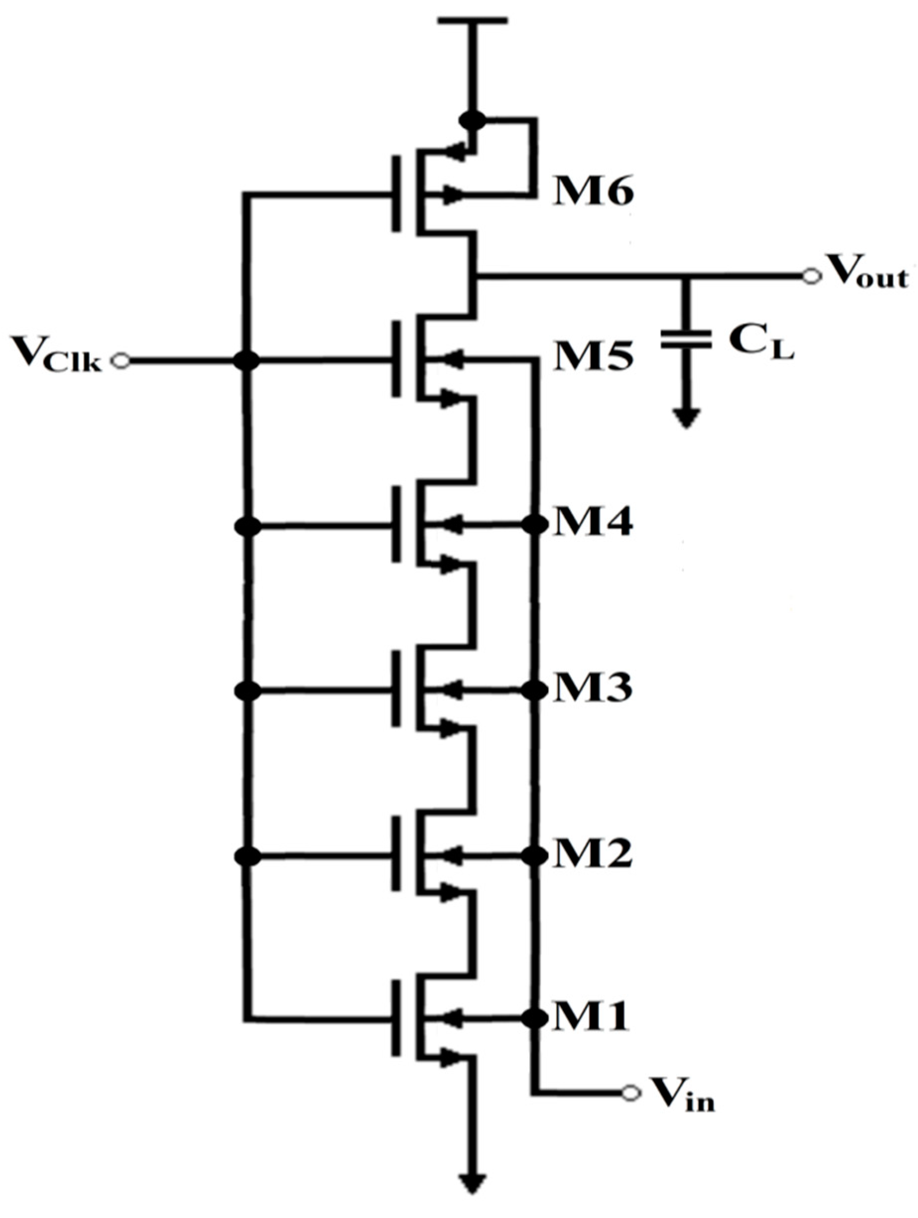
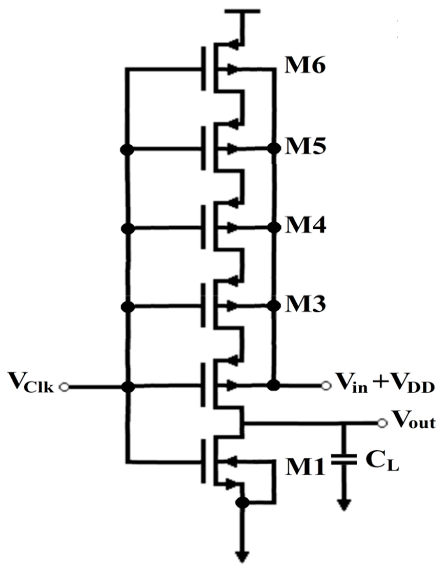
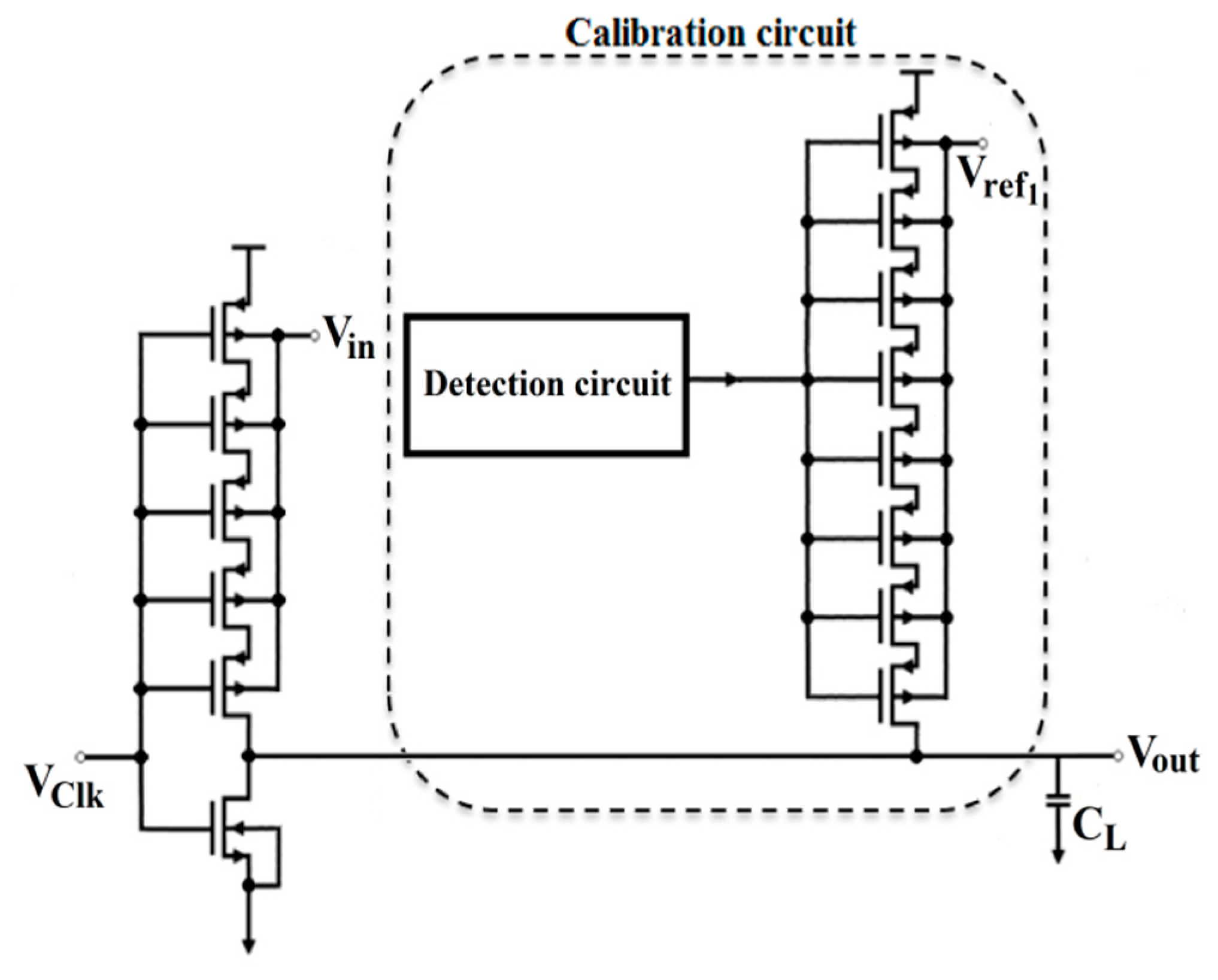
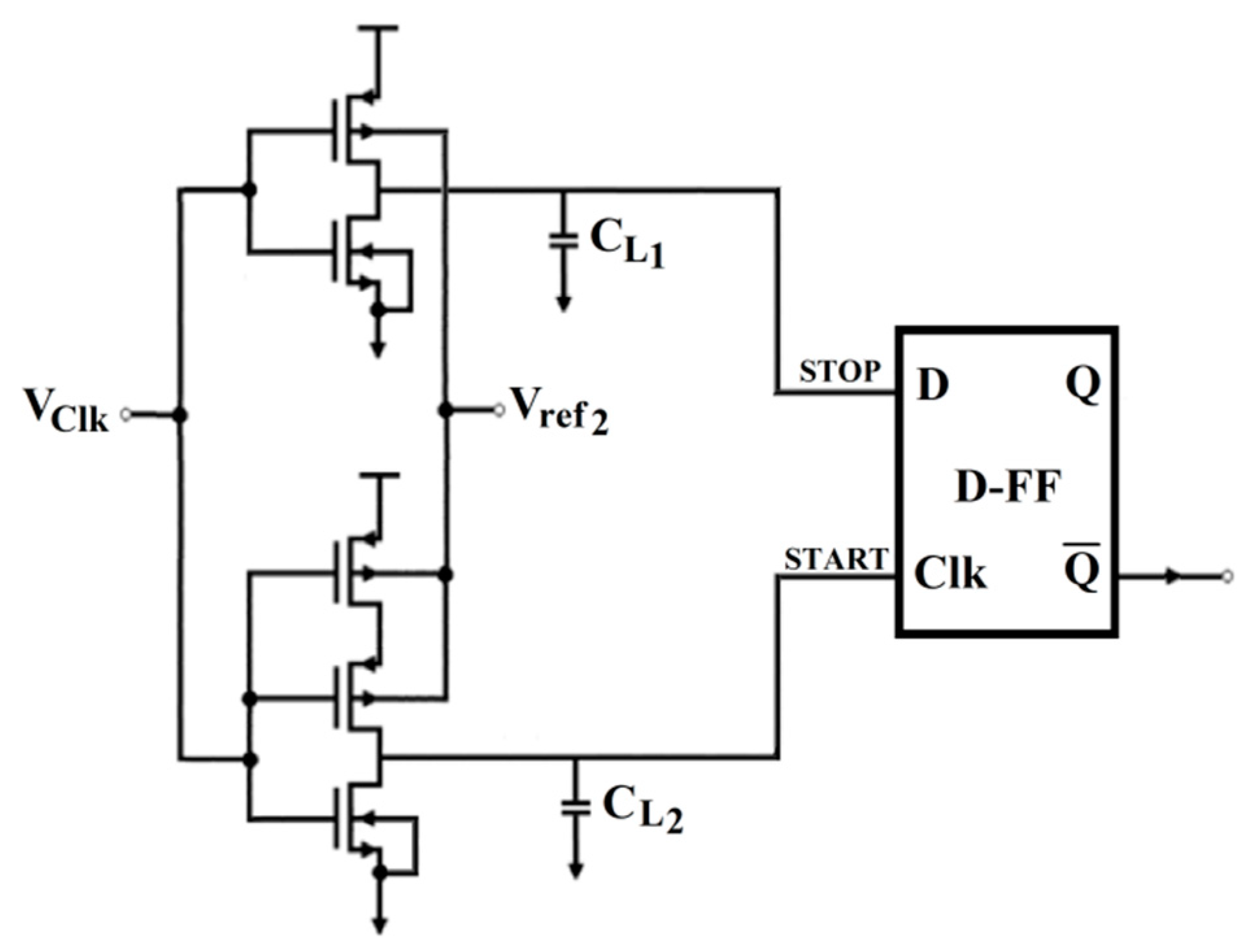
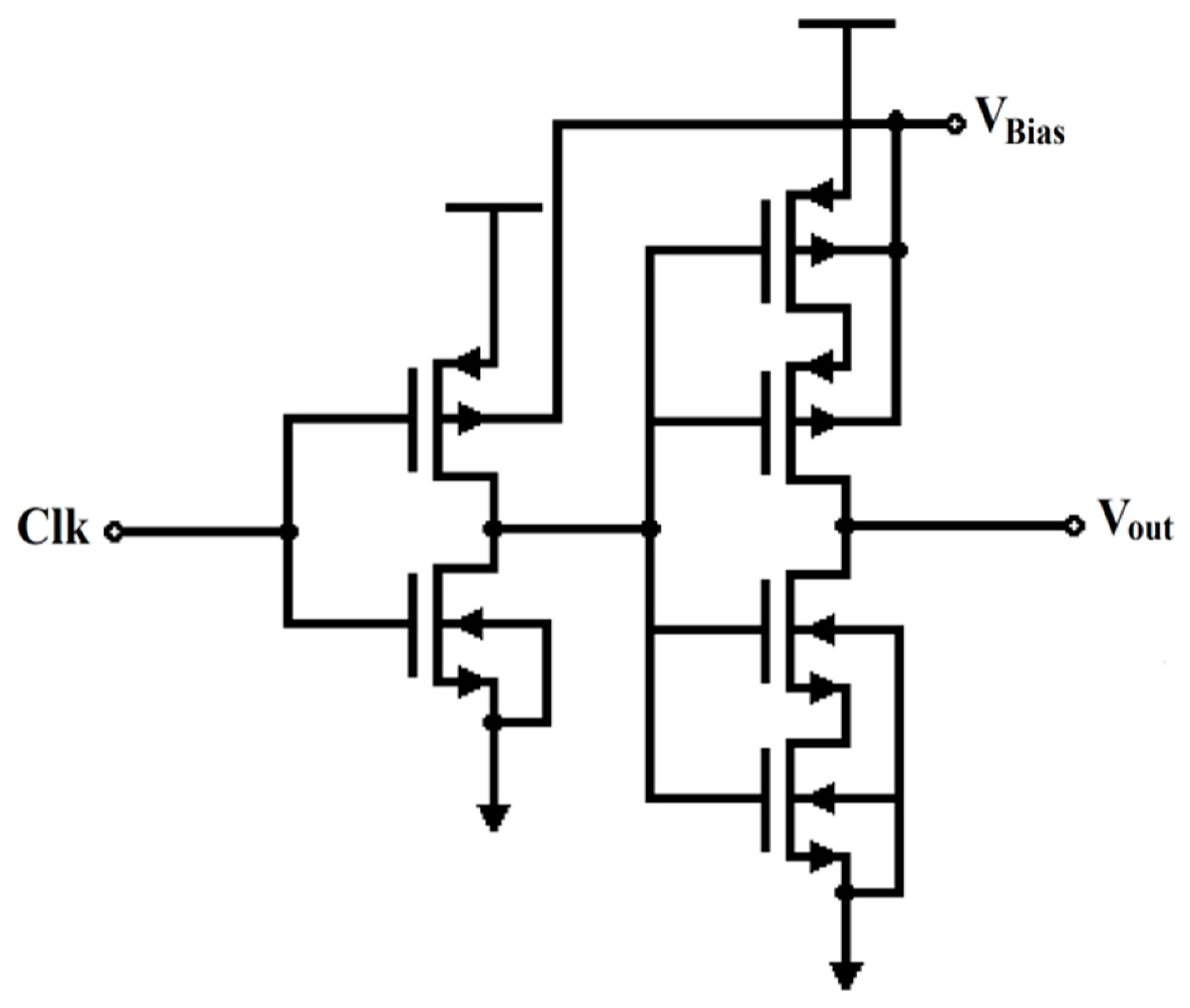
2.2. Second Proposed VTC

The second proposed VTC circuit has the same theory of operation as the first proposed VTC. However, the body biasing technique is applied on a rise-time starving inverter at which the starving transistor is PMOS. As it was proven before in the first proposed VTC, it is concluded that the rise time delay (charging time) of the output signal is linearly proportional to the input signal voltage which is applied to the body terminal.
Figure 5 shows the second proposed VTC circuit. Adding more series-identical PMOS transistors to the starving transistor helps in improving the performance of the circuit. The output delay of the proposed VTC circuit versus the number of PMOS series starving transistors (NP) is shown in Figure 6a. The maximum number of series PMOS transistors that can be used is four for a clock frequency of 500 MHz. The sensitivity of the proposed VTC is shown in Figure 6b. For a 5-bit resolution VTC, four series PMOS starving transistors are used for better sensitivity and lower quantization noise.
Figure 7 shows the final architecture of the second proposed VTC circuit. The input signal (Vin) in the second proposed VTC ranges from −0.4 to 0.4 V with an offset voltage of VDD. This offset voltage is added as the source of the starving PMOS transistor is connected to VDD keeping the body-to-source voltage (VBS) equal to Vin. This input dynamic range ensures that the body-to-source voltage does not exceed 0.4 V to avoid latching-up [18,21,22].
There are several circuits that can be used to add the supply voltage (VDD) to the input signal (Vin). One of these circuits is the non-inverting summing amplifier shown in Figure 8. In this circuit, the input signal (Vin) and the supply voltage (VDD) are connected to the positive port of the operational amplifier. The resistors used in this circuit are identical to make the output of the amplifier equal to (Vin + VDD). This circuit is implemented off-chip on the PCB (Printed Circuit Board).

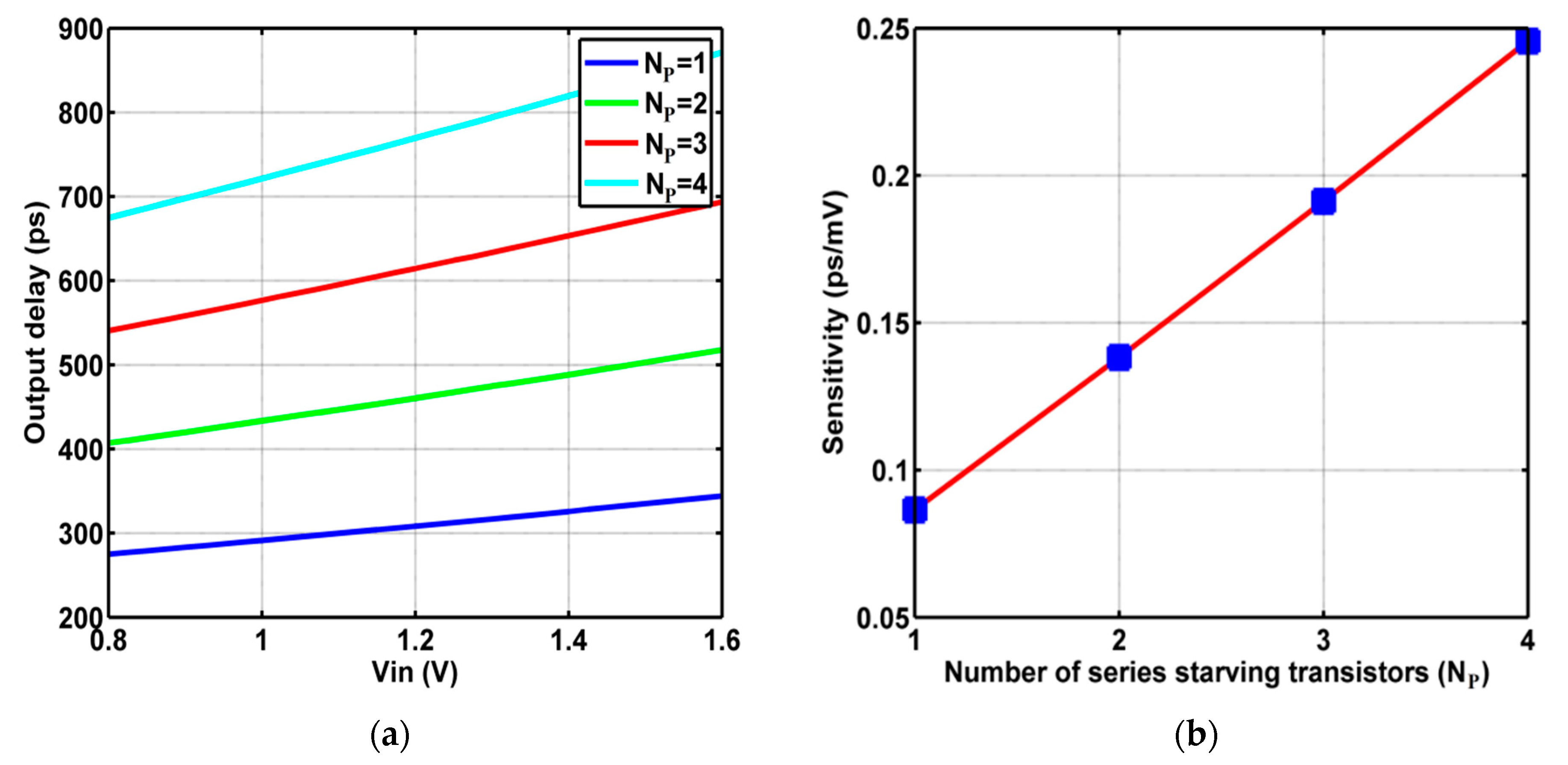
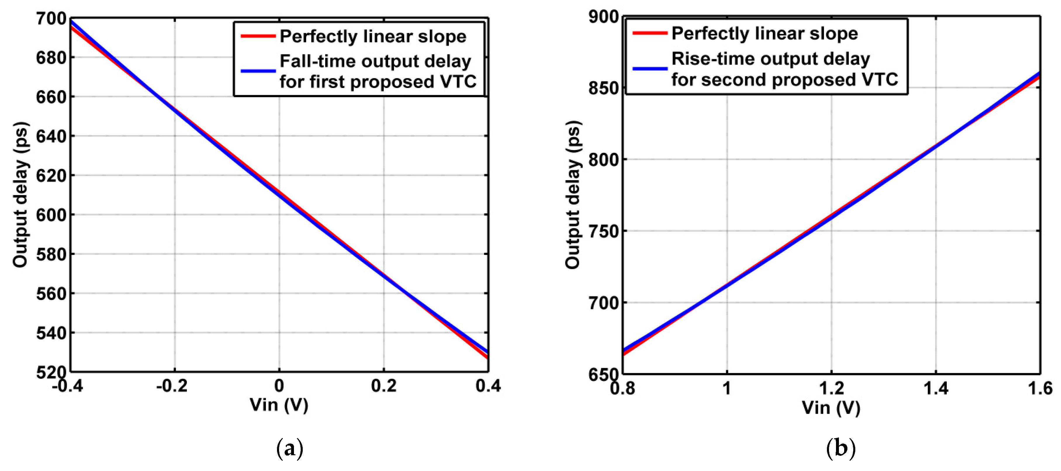
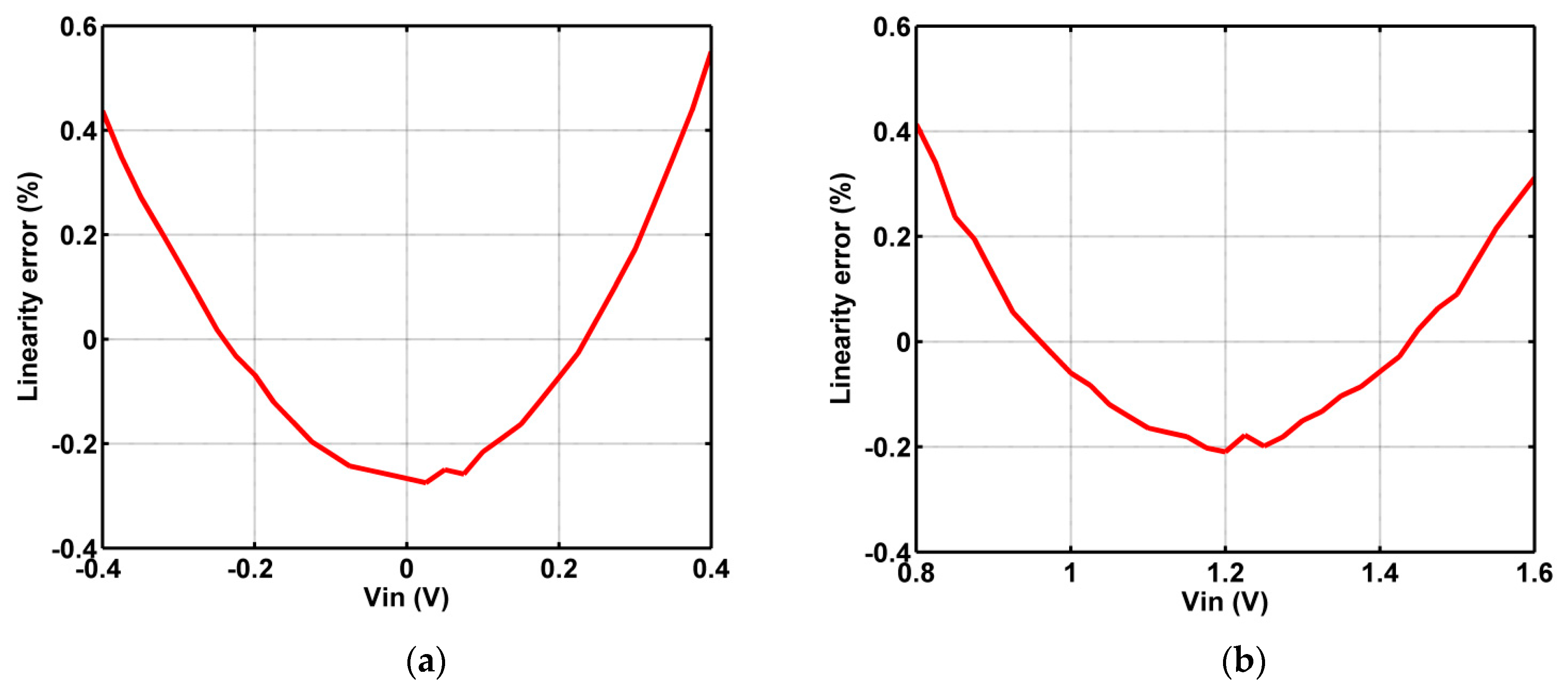
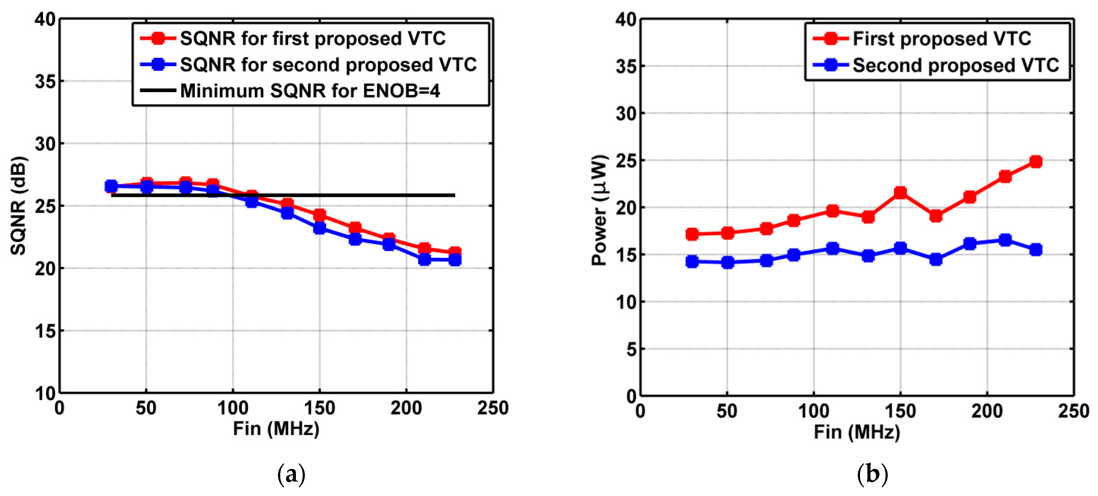
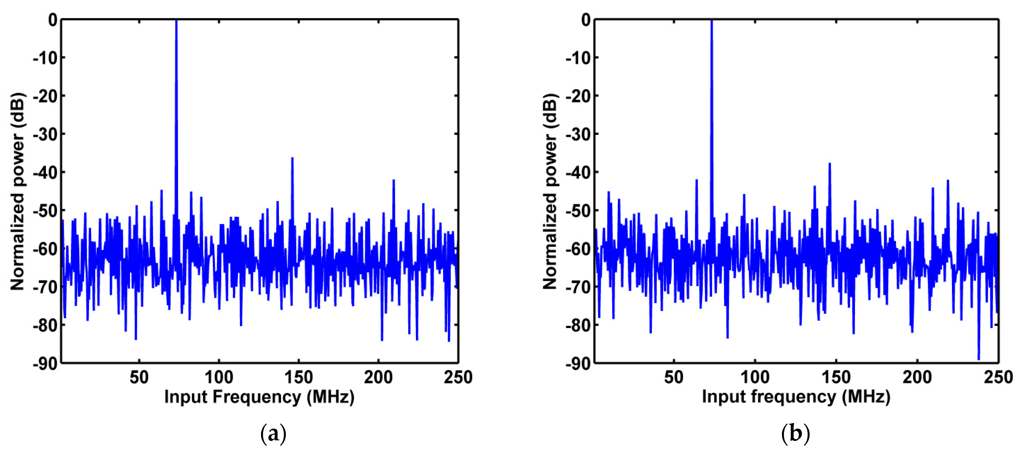
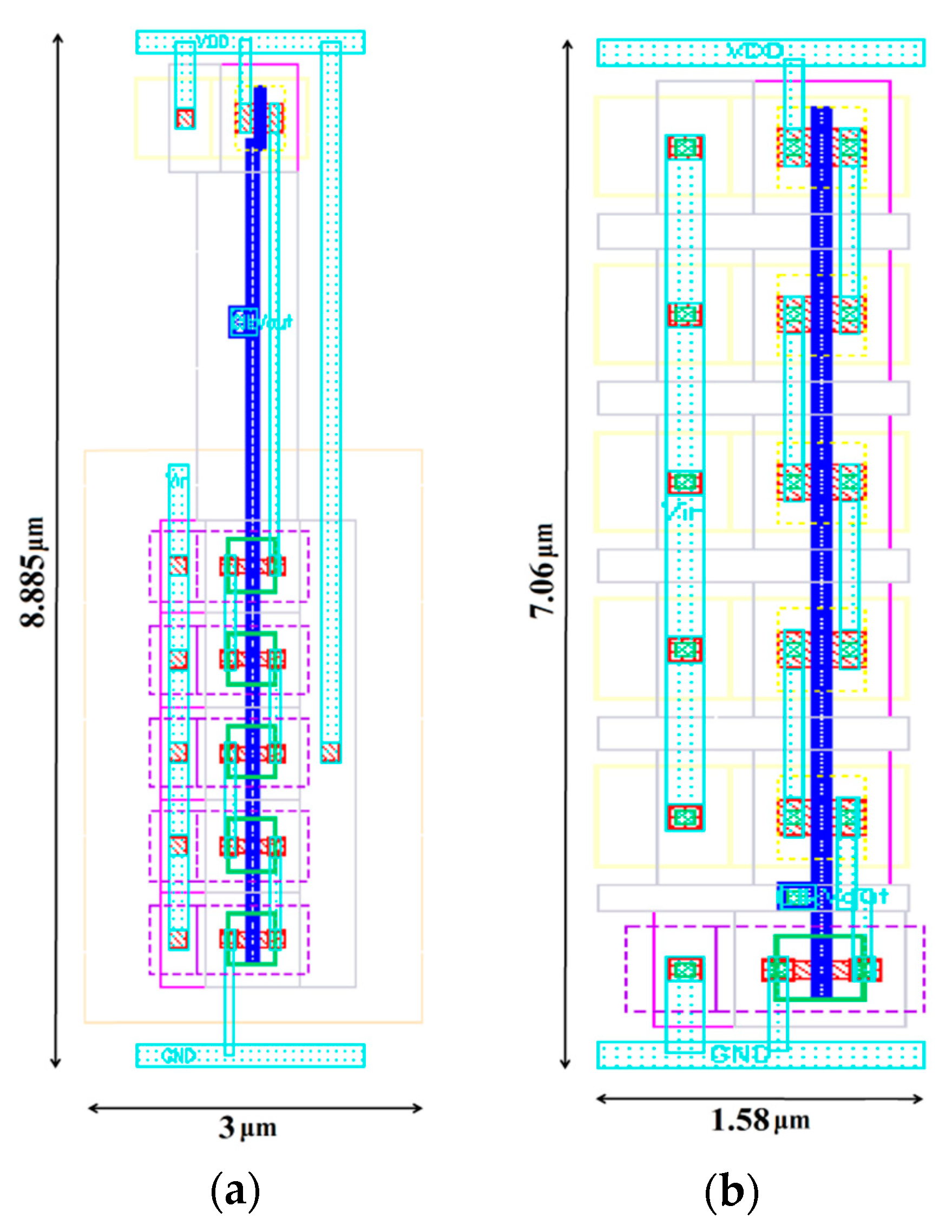
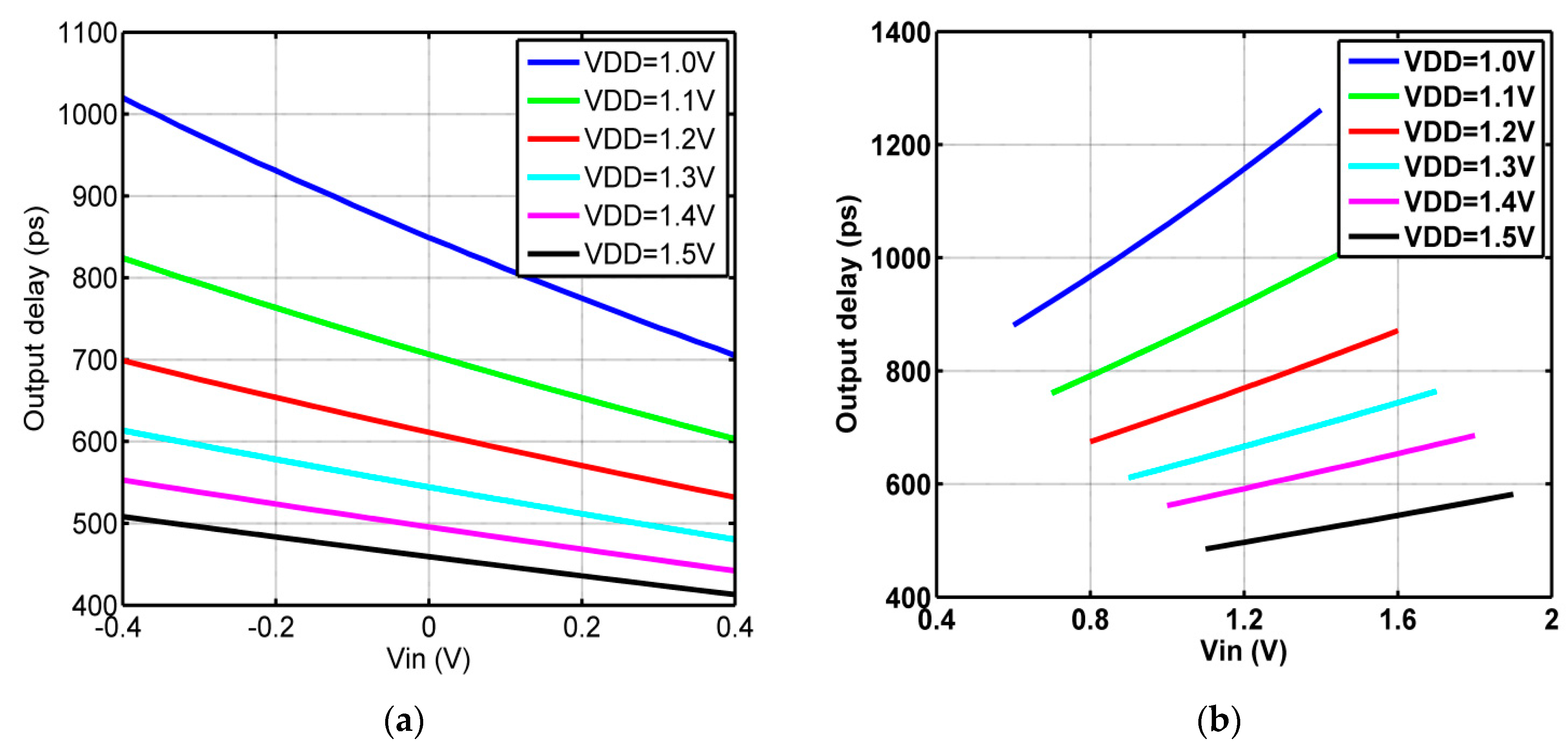
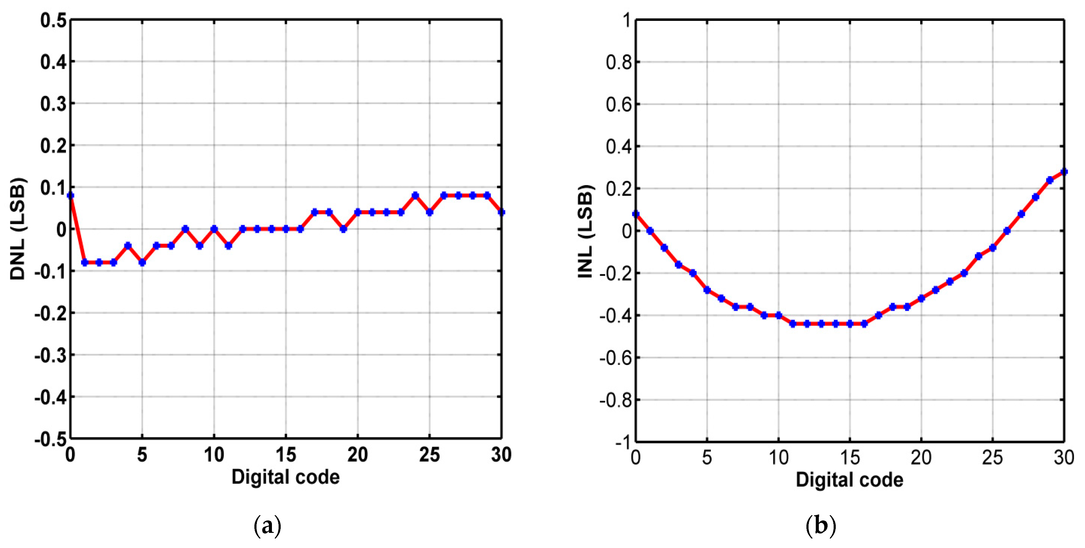
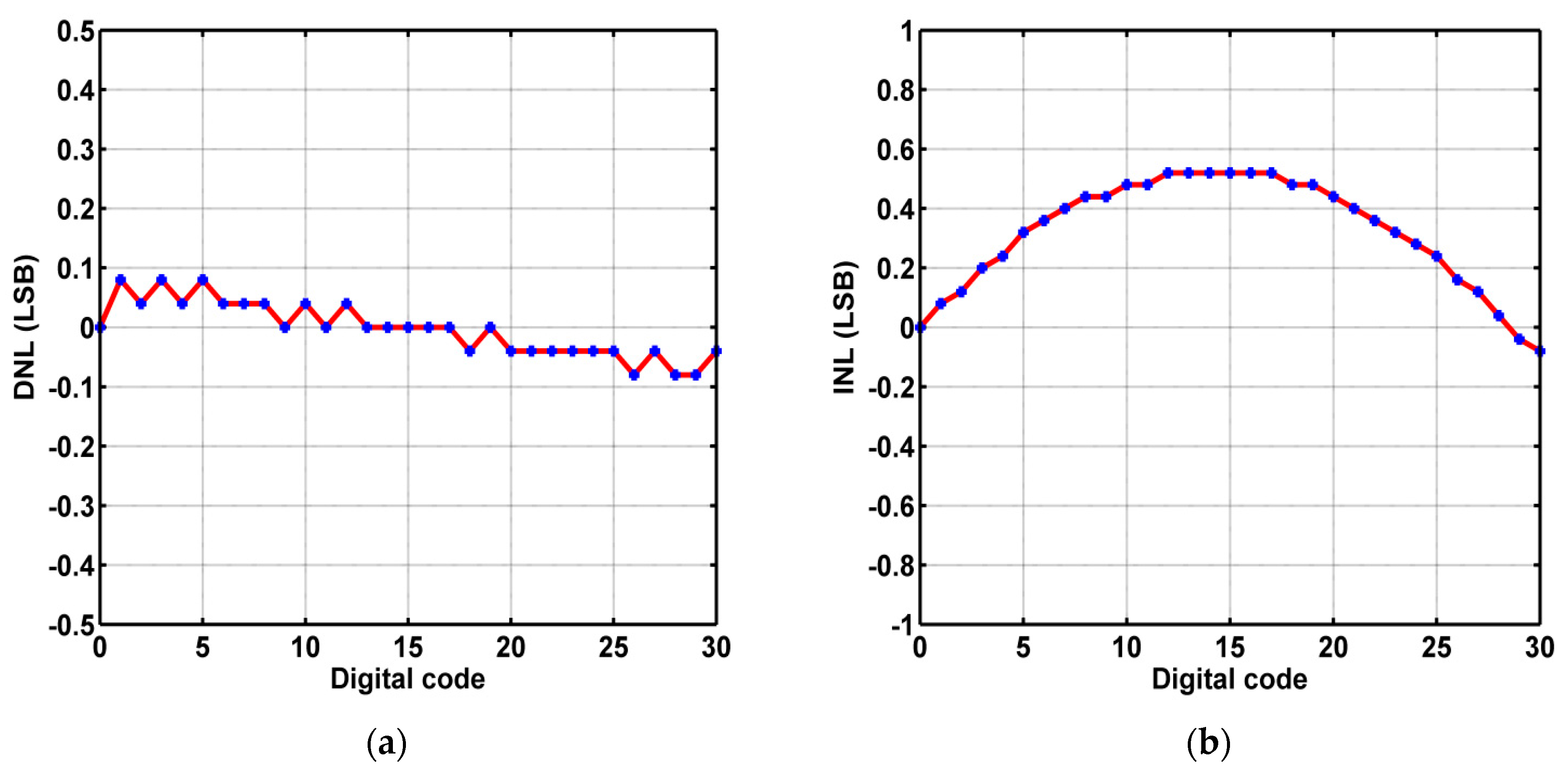
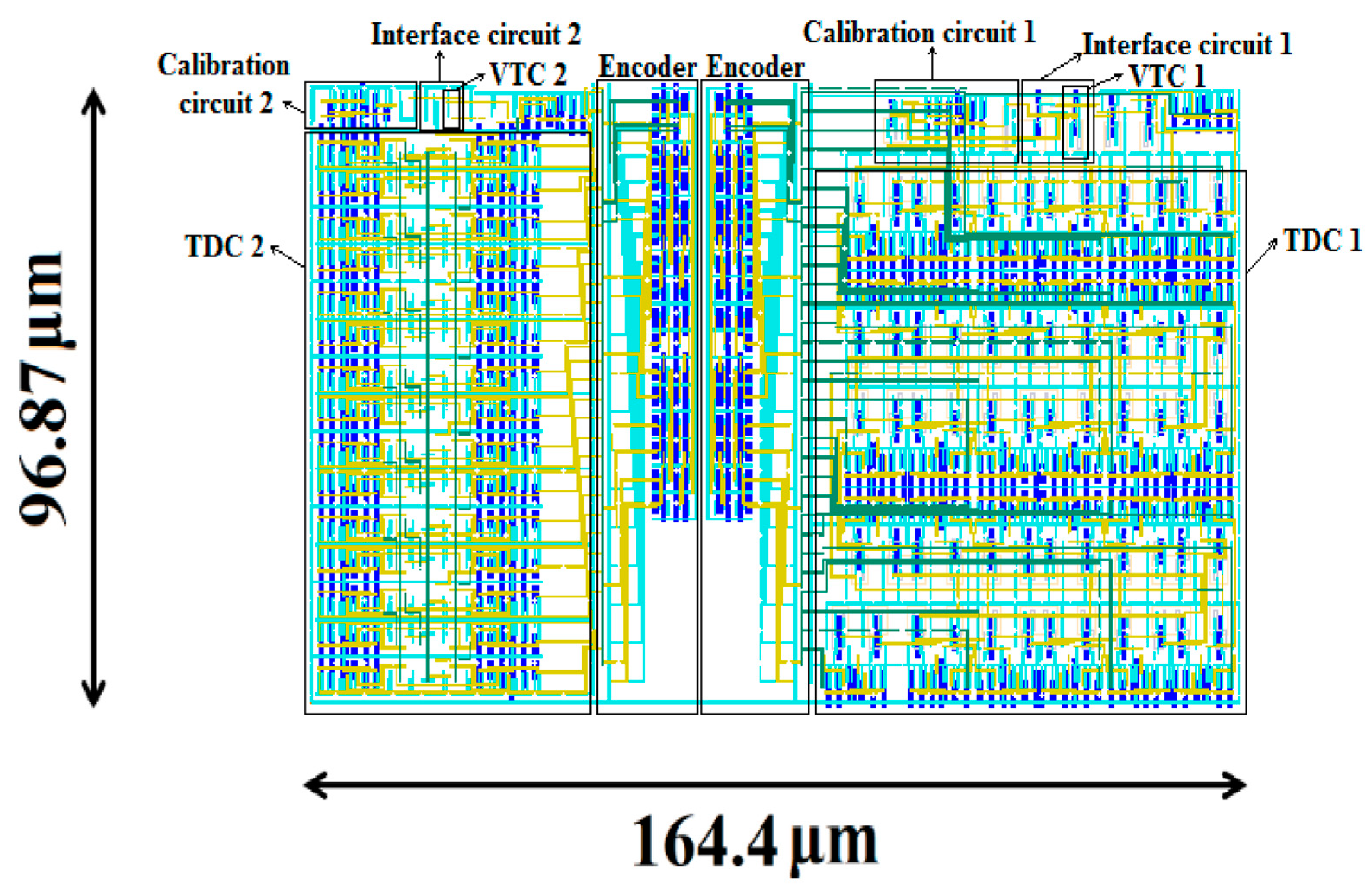
3. Simulation Results

The proposed VTC circuits are simulated using Cadence Virtuoso with industrial hardware-calibrated 65 nm transistor device models provided by TSMC. The simulation is performed using a supply voltage of 1.2 V. The Least Significant Bit (LSB), which is mainly dependent on the TDC block, is assumed to be equal to 5 ps, resulting in a resolution of 5 bits for the proposed VTC circuits. The clock frequency equals to 500 MHz and the frequency of the input signal equals to 72.75 MHz. The size of all NMOS transistors used in the two proposed designs is identical and equal to (120 nm/60 nm). This is the minimum allowable size to achieve high output delay range for better resolution. The size of all PMOS transistors is twice that for the NMOS transistor and equal to (240 nm/60 nm).
Figure 9a shows the fall time of the output delay for the first proposed VTC circuit compared with a perfectly linear slope. Moreover, Figure 9b shows the rise time of the output delay for the second proposed VTC circuit compared with a perfectly linear slope. The linearity error for each of the first and second proposed circuits is calculated and plotted in Figure 10. It is obvious that the maximum linearity error significantly decreased to about 0.55% for the first proposed VTC and about 0.4% for the second proposed VTC.
Signal-to-quantization noise ratio (SQNR) is a very important parameter that affects the ADC performance. Figure 11a shows the SQNR for different input frequencies. It is obvious that for the effective number of bits (ENOB) to be greater than four, the maximum input frequency is equal to 105 MHz for the first proposed VTC and 95 MHz for the second proposed VTC. Figure 11b shows the power consumption for the proposed VTCs at different input frequencies. It is obvious that the second proposed VTC circuit exhibits lower power consumption than that for the first proposed VTC circuit.
Figure of merit (FOM) represents the efficiency of the VTC in terms of the power consumption, sampling frequency and the input dynamic range. It can be expressed by two formulas, as follows [23]:
F O M 1 =   D R 2   F S P
F O M 2 =   P 2 E N O B F s
where DR is the input dynamic range, FS is the sampling frequency and P is the overall power consumption.
Effective number of bits (ENOB) is calculated by using the FFT (Fast Fourier Transform) method with 1024 samples for an input sinusoidal signal at a frequency of 72.75 MHz and clock frequency of 500 MHz. This specific value for the input frequency is chosen to ensure coherent sampling is achieved for more accurate results [24]. The frequency spectrums of the first and second proposed circuits are shown in Figure 12. Table 1 shows a comparison between the proposed VTC designs and other modified VTCs [25,26,27,28,29,30]. It indicates that both proposed VTCs have the minimum power consumption while having a wide dynamic input range and better FOM values. Although the design proposed in Reference [25] has a wider input range and operates at higher sampling frequencies, the power consumed by this design is much higher than that for the proposed VTCs.
The layouts of the proposed VTC circuits are shown in Figure 13. The first VTC circuit occupies 26.67 μm2, whereas the second VTC circuit occupies 11.16 μm2. Both areas for the proposed VTCs are very small compared to other VTC circuits (as shown in Table 1) thanks to their simple design (one-stage circuit). It should be highlighted that twin-well/triple-well technologies are needed for the NMOS body control in order to isolate the p-well from the p-substrate (by using deep N-well), which results in a higher layout area. This is not needed for the PMOS body control.
It should be noted that the simulations provided in this work are post-layout simulations using CAD tools and nowadays, the CAD tools are accurate enough to produce results close to the measured results, especially for mature technologies such as the 65 nm technology.
The power has been calculated taking into consideration the dynamic power as well as the leakage power. However, the proposed circuit provides low power consumption, compared to other papers in the literature, due to its novelty in using the body terminal as an analog input terminal to improve the linearity. This is because usually, the body terminal carries very low current and accordingly, adds insignificant power consumption [18,21].
The proposed VTCs exhibit a significant performance in terms of linearity, power consumption and dynamic range. The proposed VTCs exhibit a maximum linearity error of 0.55% for a wide input dynamic range of 800 mV. The proposed VTCs have very low power consumption due to their simple circuit design, which also results in exhibiting a small chip area. However, the proposed VTCs suffer from low resolution and quite low sampling frequencies. The proposed designs are suitable for applications with limited power budget, such as internet of things (IoT) and wearable devices. In addition, the proposed VTC circuits can be applied for low-resolution ADCs for wireless communication receivers in multiple-input multiple-output (MIMO) systems as the power consumption is a much more important factor than resolution [31,32,33].
Many research results show that low-resolution quantization technology provides allowable channel capacity loss [31]. Moreover, it is claimed that low-resolution ADCs are better used in massive multi-user MIMO systems as they provide better throughput than that with high-resolution ADCs while keeping the power consumption at lower levels [32,33].

4. Discussion

There are important factors that affect the performance of the proposed VTC circuits. These factors are process-voltage-temperature (PVT) variations, time-to-digital converter (TDC), differential non-linearity (DNL), integral non-linearity (INL) and jitter.

4.1. Process-Voltage-Temperature (PVT) Variations

4.1.1. Process Variations

Process variations are very important factors that measure the performance of the VTC circuit. They affect the output delay of the circuit. Hence, the linearity of the VTC and ENOB are also affected. The performance of the proposed circuits is investigated in terms of maximum linearity error, sensitivity and ENOB for the three main process corners TT, FF and SS, as shown in Table 2. It is obvious that the sensitivity at SS corner increases to 0.405 ps/mV for the first proposed VTC and 0.424 ps/mV for the second proposed VTC. However, the maximum linearity error at SS corner increases to 1.3% for the first proposed VTC and 0.961% for the second proposed VTC.
The clock frequency used at process corners is reduced to 400 MHz as the output delay at SS corner exceeds 1 ns. Moreover, the input signal frequency is chosen to be nearly equal to 61.33 MHz to ensure coherent sampling is achieved. Coherent sampling guarantees that FFT results are accurate for proper calculation of ENOB. ENOB decreases to 3.5 bits at SS corner for the first proposed VTC and decreases to 3.6 bits for the second proposed VTC. As a result, calibration for the proposed circuits is needed to improve the linearity and ENOB for the proposed circuits at SS corner.
A calibration circuit for the first proposed VTC is proposed to improve the performance of the VTC at SS corner. The first proposed VTC and the calibration circuit are shown in Figure 14. The calibration circuit consists of a detection circuit and a stack of eight identical NMOS transistors connected between the output node of the VTC and the ground node. The function of the detection circuit is to detect the occurrence of SS corner.
The detection circuit is shown in Figure 15. It consists of two inverters with different load capacitors and a D Flip-Flop (D-FF). The values of the load capacitances are adjusted such that the START signal edge comes before the STOP signal edge only when the circuit operates at SS corner. In this case, the inverted output of the D-FF (Q-bar) will be “1”.
The output of the D-FF activates the stack of NMOS transistors which results in increasing the discharging current of the load capacitance at the output node. This leads to a significant decrease in the output delay range at SS corner to be near the range obtained at the nominal corner TT. The value of the reference voltage (Vref) is set to −0.4 V, which is the minimum allowed voltage. This allows the stack to drive a small current to keep the output sensitivity at acceptable levels at SS corner.
The detection circuit detects only SS corners and the inverted output of the D-FF keeps its state at ‘0’ for TT and FF corners. Moreover, the values of the load capacitances are adjusted such that the state of the inverted output of the D-FF is ‘0’ even if the circuit is subjected to temperature variations. This can be easily achieved as the additional delay produced from temperature variations is less than that at SS corner.
Table 3 shows the change in the performance of the first proposed VTC circuit before and after calibration at process corners. The maximum linearity error at SS corner improved after calibration to be equal to 0.38%. ENOB is also improved to be equal to 4.38 at SS corner after calibration. Although sensitivity is decreased at SS corner after calibration, it becomes near to that value at the nominal process corner. The value of the load capacitance CL1 equals 30 fF and the value of the load capacitance CL2 equals 55 fF.
The second proposed VTC circuit is calibrated by the same technique. Figure 16 shows the calibrated second proposed VTC circuit. The calibration circuit consists of a detection circuit and a stack of eight identical PMOS transistors connected between the supply voltage and the output node of the VTC.
Figure 17 shows the detection circuit. It has the same theory of operation as in the detection circuit of the first proposed VTC. It detects the occurrence of SS corner at which the output of D-FF will be ‘0′ at this corner only. This activates the stack to increase the charging current of the load capacitance at the output node. Similarly, the value of the reference voltage (Vref 1) is set to 1.6 V. This allows the stack to drive a small current to keep the output sensitivity at acceptable levels at SS corner. The value of the load capacitance CL1 equals 60 fF and the value of the load capacitance CL2 equals 30 fF. The value of the reference voltage (Vref 2) is set to 0.8 V.
Table 4 shows the change in the performance of the second proposed VTC circuit before and after calibration at process corners. The maximum linearity error at SS corner improved after calibration to be equal to 0.26%. ENOB is also improved to be equal to 4.35 at SS corner after calibration. The sensitivity of the second proposed VTC at SS corner after calibration becomes near to the value at TT process corner. All the NMOS transistors used in the calibration circuits are identical to each other, having the size of (120 nm/60 nm). In addition, all the PMOS transistors used are identical to each other, having the size of (240 nm/60 nm).

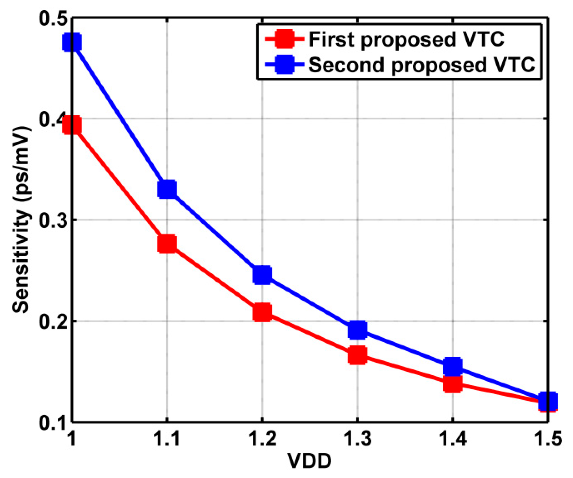
4.1.2. Supply Voltage Variations

The supply voltage is one of the most important factors that affect the performance of the VTC circuit. The VTC output delay is calculated for different supply voltages for the two proposed VTC circuits, as shown in Figure 18.
As the supply voltage decreases, the output delay range increases, which results in increasing the sensitivity of the proposed VTC circuits, as shown in Figure 19. However, reducing the supply voltage results in degradation of the signal-to-noise ratio (SNR) that limits the performance of the whole ADC circuit [1].

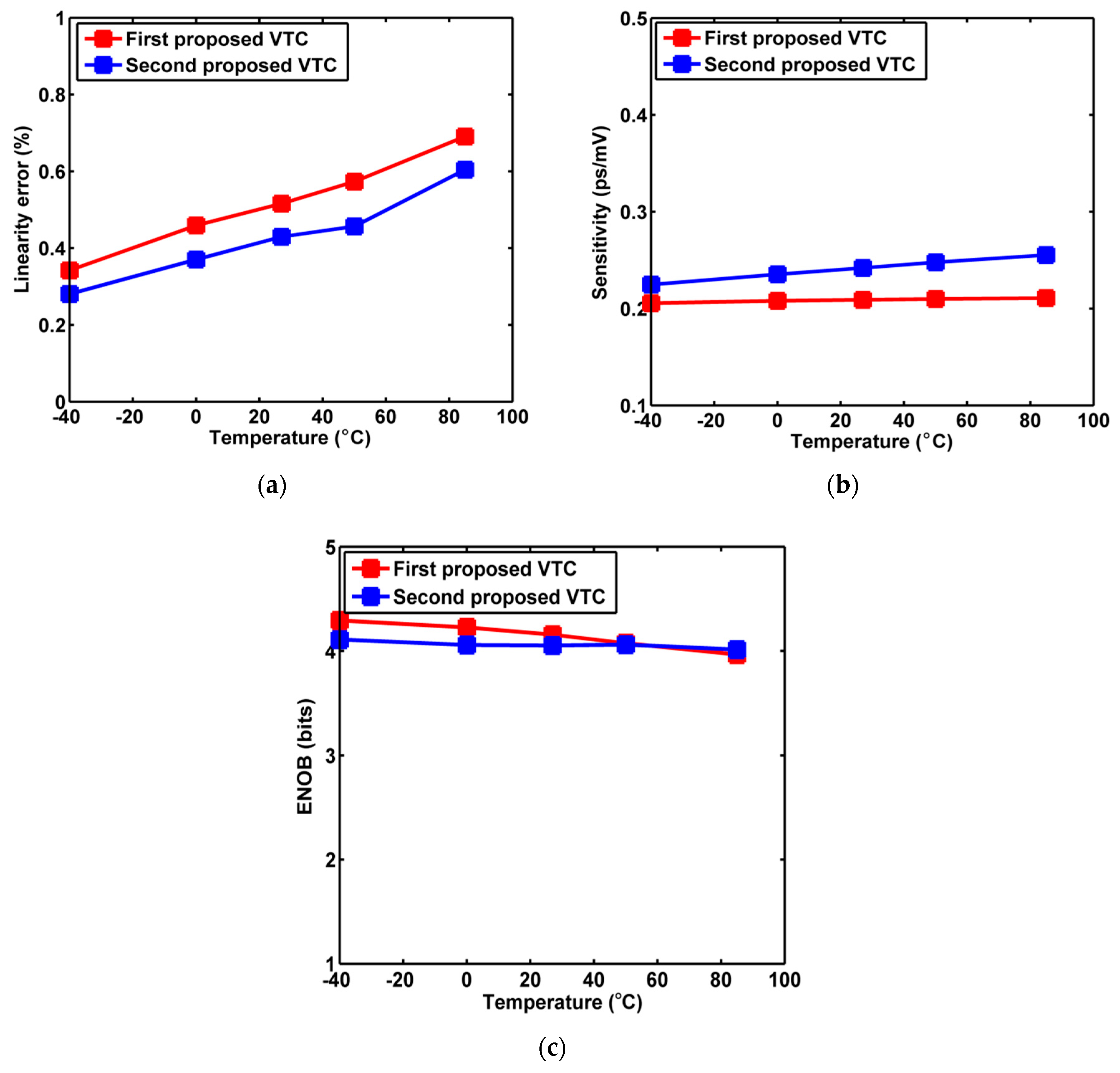
4.1.3. Temperature Variations

Temperature variations have a significant effect on the operation speed of integrated circuits. As the temperature increases, the current driven by transistors decreases, causing additional latency to the output of the circuit. The effect of temperature variations on the linearity, sensitivity and ENOB of the proposed VTC circuits is investigated for a temperature range from −40 to 85 °C. Figure 20a shows the maximum linearity error versus temperature variations for the two proposed circuits. It is obvious that although the maximum linearity error increases with temperature, it does not exceed 1% for the given temperature range. The sensitivity of the proposed VTC circuits shows a slight increase by increasing the temperature, as shown in Figure 20b. Moreover, ENOB for the proposed VTC circuits keeps its value at an acceptable level for the given temperature range, as shown in Figure 20c. The input signal frequency is chosen to be nearly equal to 61.33 MHz at a clock frequency of 400 MHz. In sum, it is obvious that the two proposed VTC circuits show immunity in terms of linearity, sensitivity and ENOB against temperature variations and do not need calibration.

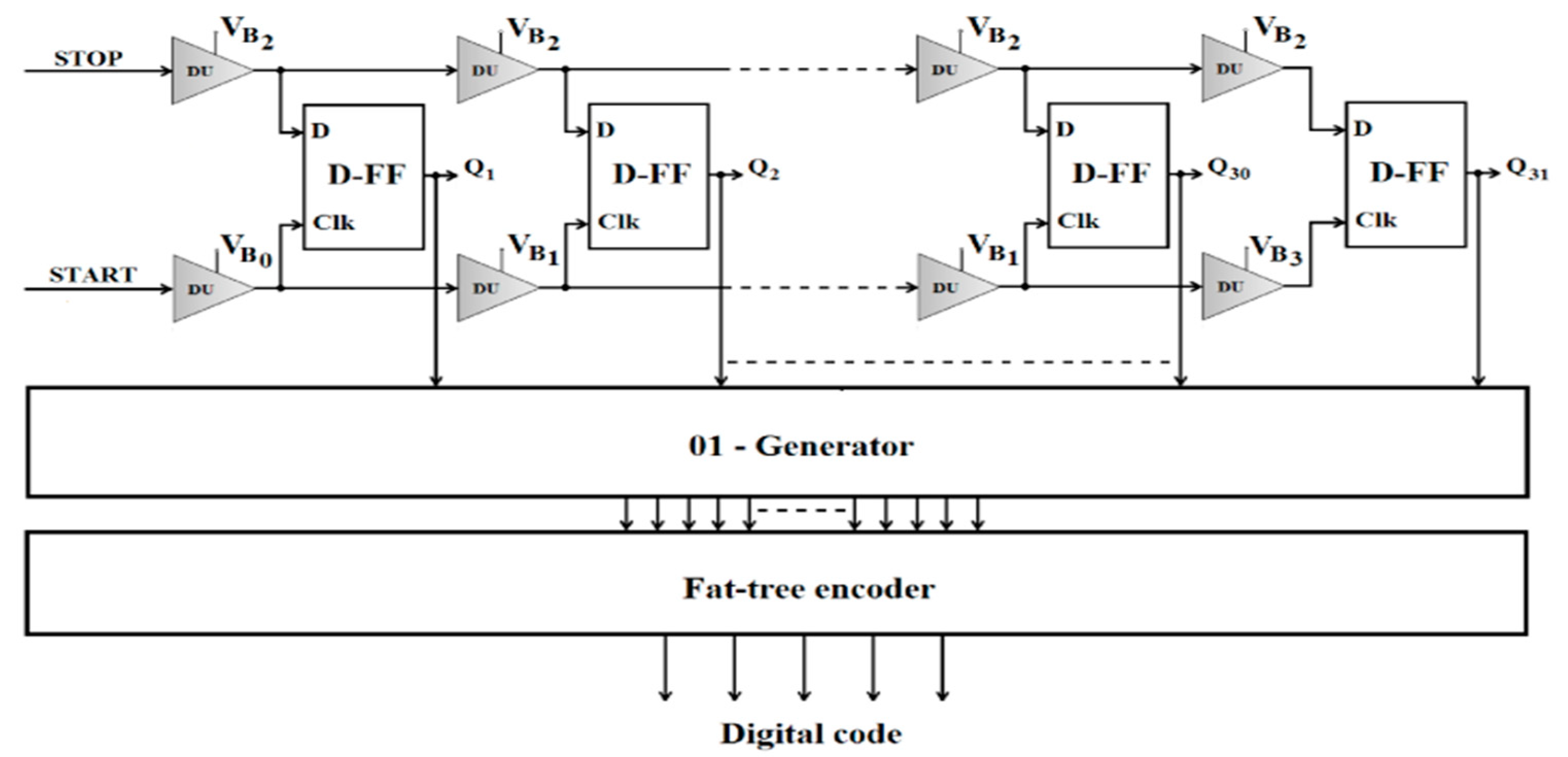
4.2. Time-To-Digital Converter (TDC)

The performance of the VTC is limited by the design of the time-to-digital converter (TDC) circuit that follows it. The TDC affects the linearity of the whole ADC and its performance should be investigated. Differential non-linearity (DNL) and integral non-linearity (INL) are the most important parameters that represent the linearity in the whole ADC. DNL represents the deviation in the conversion step of the ADC from its ideal value (1 LSB), while INL represents the deviation of the whole transfer function of the ADC from its ideal value [34]. DNL value should not exceed 1 LSB in order to avoid missing codes [34]. Thus, each of the two proposed VTC circuits is implemented with a 5-bit vernier delay-line TDC and the whole ADC is simulated.
For the first proposed VTC, an interface circuit is proposed after the VTC in order to drive STOP and START signals to the TDC. Figure 21 shows the interface circuit that is used for the first proposed VTC. The output of the VTC is inverted to produce the START signal. The STOP signal is a delayed version of the clock signal. The delay unit for the STOP signal is the VTC circuit with a reference voltage equivalent to the maximum delay that can be produced from the VTC (Vref = −0.4 V).
A standard vernier delay-line TDC is used in this work. It is most commonly used as it has the advantage of having very high resolution that can be less than the minimum gate delay in the technology used. However, this resolution is limited by other factors such as noise, transistors’ mismatch and the delay-line physical length [35]. Many TDC circuits based on the vernier delay-line technique are proposed [36,37,38,39] to achieve higher resolution that can reach 3.2 ps [40], 2 ps [41] or even more.
Figure 22 shows a 5-bit vernier delay-line. The delay units (DUs) are CMOS buffers which are controlled by controlling the body-to-source voltage, as shown in Figure 23. When the input signal value is minimum, the START signal comes after the STOP signal for all the D-FFs in the TDC and the output of all the flip-flops is ‘1’. On the other hand, when the input signal value is maximum, the START signal comes before the STOP signal for all the D-FFs in the TDC and the output of all the flip-flops is ‘0’. By varying the input signal, the output of the flip-flops will also vary. The output of the flip-flops is an inverted thermometer code. The thermometer code is first converted to a one-hot code using 01-generator circuits [42]. The 01-generator circuit is shown in Figure 24. Then, a digital code is generated using a fat tree encoder [43].
The TDC is manually calibrated by adjusting the biasing voltages for the delay units. The values of the biasing voltages after calibration are VB2 = 0.4 V, VB1 = 0.075 V, VB0 = 0.39 V and VB3 = 0.2 V. DNL and INL are calculated for the ADC with accuracy of 1 mV (800 points are calculated for 800 mV input range). This means each digital code has 25 calculated points (LSB = 25 mV). Figure 25 shows DNL and INL for the first proposed ADC. The maximum DNL equals ±0.08 LSB and INL equals 0.28 LSB (maximum INL equals −0.44 LSB).
For the second proposed VTC, the interface circuit is modified, at which the START and STOP signals are replaced by each other. Moreover, the inverters are replaced by buffers as the output delay of the VTC is a rise time. In addition, the reference voltage used equals 0.8 V, which is equivalent to the minimum output delay of the second proposed VTC. The interface circuit for the second proposed VTC is shown in Figure 26.
The same TDC is used for the second proposed VTC and the delay units are controlled by controlling the body-to-source voltage, as shown in Figure 27. The theory of operation is the same as previously discussed for the first proposed circuit. After calibration, the values of the biasing voltages are VB2 = 1 V, VB1 = 1.45 V, VB0 = 0.95 V and VB3 = 1.6 V.
Figure 28 shows DNL and INL for the second proposed ADC. They are calculated with accuracy of 1 mV. The maximum DNL equals ±0.08 LSB and INL equals −0.08 LSB (maximum INL equals 0.52 LSB).
In sum, the two proposed VTC circuits exhibit high performance when implemented with vernier delay-line TDC to construct the whole ADC circuit. DNL and INL for the proposed designs are compared with other modified designs in Table 1. It is obvious that the proposed designs have better DNL and INL results. All the NMOS transistors used in the interface circuit and the TDC are identical to each other, having the size of (120 nm/60 nm). In addition, all the PMOS transistors used are identical to each other, having the size of (240 nm/60 nm).
Figure 29 shows the layout of the two proposed ADCs. The layout includes the two proposed VTCs, the calibration circuits, the interface circuits and the TDC circuits. The first ADC occupies an area of 0.0092 mm2, while the second ADC occupies an area of 0.0067 mm2. The first ADC occupies a higher area than the second ADCs due to using triple-well technology (deep N-well layer) for the NMOS body control.

4.3. Jitter

Jitter in VTC represents the random deviation of the output delay signal in the time domain from its ideal value. This shift resulted from random noise. There are possible sources of noise in the proposed VTC circuit that produce this jitter. These sources are thermal noise from the device, noise from the supply lines, noise from the input signal and noise from the following TDC block [5,24]. By considering the jitter effect during simulation of the proposed VTC circuits using transient noise analysis, it is concluded that jitter has an insignificant effect on linearity, sensitivity and ENOB. This is because the circuit is operating at moderate frequency and accordingly, the proposed VTC circuits tolerate the jitter. However, this places a limitation on the proposed VTC if used at high frequencies as the jitter might have a significant effect in this high-frequency case.
For the first proposed VTC, maximum linearity error is 0.55%, and sensitivity equals 0.2108. These values do not change significantly with jitter. ENOB equals 4.163 at Fin = 73.73 MHz and FClk = 500 MHz, and changes to 4.108 when jitter is considered. For the second proposed VTC, maximum linearity error is 0.4%, and sensitivity equals 0.243. These values do not change with jitter. ENOB equals 4.093 at Fin = 73.73 MHz and FClk = 500 MHz, and changes to 4.049 after taking jitter into account.

5. Conclusions

In this paper, two novel VTC circuits were proposed achieving better linearity with wide input dynamic range. The input signal was connected to the body terminal of the starving transistor instead of its gate terminal. The maximum linearity error was 0.55% for the first proposed VTC and 0.4% for the second proposed VTC, with an input dynamic range of 800 mV for a supply voltage of 1.2 V. The proposed VTCs can be used for a 5-bit time-based ADC at a maximum sampling frequency of 500 MHz in 65 nm CMOS technology. Thanks to their simple design, the proposed VTC circuits occupy a small area of 26.67 μm2 for the first proposed VTC and 11.16 μm2 for the second proposed VTC, while consuming very small power of 18 μW for the first proposed VTC and 15 μW for the second proposed VTC. The effect of PVT variations on the proposed designs was discussed. In addition, calibration circuits were proposed to overcome the limitations in the VTC circuits’ performance due to these variations. Moreover, time-to-digital converter (TDC) and the jitter effect were discussed.

Author Contributions

Conceptualization, A.D., H.M. and E.-s.E.-R.; methodology, H.M. and A.E.; software, A.E.; validation, E.-s.E.-R., H.M. and R.A.; formal analysis, A.D., R.A. and A.E.; investigation, A.E.; data curation, E.-s.E.-R. and H.M.; writing—original draft preparation, A.E. and R.A.; writing—review and editing, H.M., R.A. and A.E.; supervision, E.-s.E.-R. and H.M. All authors have read and agreed to the published version of the manuscript.

Funding

This research received no external funding.

Conflicts of Interest

The authors declare no conflict of interest.

References

  1. Mostafa, H.; Ismail, Y.I. Highly-linear voltage-to-time converter (VTC) circuit for time-based analog-to-digital converters (T-ADCs). In Proceedings of the 2013 IEEE 20th International Conference on Electronics, Circuits, and Systems (ICECS), Abu Dhabi, UAE, 8–11 December 2013; pp. 149–152. [Google Scholar]
  2. Hassan, A.H.; Ismail, M.W.; Ismail, Y.; Mostafa, H. A 200 MS/s 8-bit Time-Based Analog-to-Digital Converter with Inherit Sample and Hold. In Proceedings of the 2016 29th IEEE International System-on-Chip Conference (SOCC), Seattle, WA, USA, 6–9 September 2016; pp. 120–124. [Google Scholar]
  3. Pekau, H.; Yousif, A.; Haslett, J.W. A CMOS integrated linear voltage-to-pulse-delay-time converter for time based analog-to-digital converters. In Proceedings of the 2006 IEEE International Symposium on Circuits and Systems (ISCAS), Island of Kos, Greece, 21–24 May 2006; pp. 2373–2376. [Google Scholar]
  4. Macpherson, A.R.; Townsend, K.A.; Haslett, J.W. A 5GS/s voltage-to-time converter in 90nm CMOS. In Proceeding of 2009 European Microwave Integrated Circuits Conference (EuMIC), Rome, Italy, 28–29 September 2009; pp. 254–257. [Google Scholar]
  5. Macpherson, A.R.; Townsend, K.A.; Haslett, J.W. A 2.5GS/s 3-bit time-based ADC in 90 nm CMOS. In Proceedings of the 2011 IEEE International Symposium of Circuits and Systems (ISCAS), Rio de Janeiro, Brazil, 15–18 May 2011; pp. 9–12. [Google Scholar]
  6. Naraghi, S.; Courcy, M.; Flynn, M.P. A 9-bit, 14 μW and 0.06 mm2 Pulse Position Modulation ADC in 90 nm Digital CMOS. IEEE J. Solid-State Circuits 2010, 45, 1870–1880. [Google Scholar] [CrossRef]
  7. Hassan, A.H.; Ali, A.; Ismail, M.W.; Refky, M.; Ismail, Y.; Mostafa, H. A 1 GS/s 6-bit Time-Based Analog-to Digital Converter (T-ADC) for Front-End Receivers. In Proceedings of the 2017 IEEE 60th International Midwest Symposium on Circuits and Systems (MWSCAS), Boston, MA, USA, 6–9 August 2017; pp. 1605–1608. [Google Scholar]
  8. Zhu, S.; Xu, B.; Wu, B.; Soppimath, K.; Chiu, Y. A Skew-Free 10 GS/s 6 bit CMOS ADC With Compact Time-Domain Signal Folding and Inherent DEM. IEEE J. Solid-State Circuits 2016, 51, 1785–1796. [Google Scholar] [CrossRef]
  9. Miki, T.; Miura, N.; Mizuta, K.; Dosho, S.; Nagata, M. A 500MHz-BW −52.5dB-THD Voltage-to-Time Converter utilizing a two-step transition inverter. In Proceedings of the ESSCIRC Conference 2016: 42nd European Solid-State Circuits Conference, Lausanne, Switzerland, 12–15 September 2016; pp. 141–144. [Google Scholar]
  10. Vlassis, S.; Felouris-Panetas, O.; Souliotis, G.; Plessas, F. Linear Current-to-Time Converter. In Proceedings of the 2019 14th International Conference on Design Technology of Integrated Systems in Nanoscale Era (DTIS), Mykonos, Greece, 16–18 April 2019; pp. 1–5. [Google Scholar]
  11. Samimian, N.; Mousazadeh, M.; Khoie, A. A Time-based All-Digital Analog to Digital converter for IOT Applications. In Proceedings of the 2019 27th Iranian Conference on Electrical Engineering (ICEE), Yazd, Iran, 30 April–2 May 2019; pp. 249–252. [Google Scholar]
  12. Rivandi, H.; Shakibaee, F.; Saberi, M. A 6-bit 100-MS/s Fully-Digital Time-Based Analog-to-Digital Converter. In Proceedings of the 2019 27th Iranian Conference on Electrical Engineering (ICEE), Yazd, Iran, 30 April–2 May 2019; pp. 412–415. [Google Scholar]
  13. Unnikrishnan, V.; Vesterbacka, M. Time-Mode Analog-to-Digital Conversion Using Standard Cells. IEEE Trans. Circuits Syst. I Regul. Pap. 2014, 61, 3348–3357. [Google Scholar] [CrossRef] [Green Version]
  14. Jayaraj, A.; Danesh, M.; Chandrasekaran, S.T.; Sanyal, A. Highly Digital Second-Order ΔΣ VCO ADC. IEEE Trans. Circuits Syst. I Regul. Pap. 2019, 66, 2415–2425. [Google Scholar] [CrossRef]
  15. Aiello, O.; Crovetti, P.; Alioto, M. Fully Synthesizable Low-Area Analogue-to-Digital Converters With Minimal Design Effort Based on the Dyadic Digital Pulse Modulation. IEEE Access 2020, 8, 70890–70899. [Google Scholar] [CrossRef]
  16. Wu, T.; Chen, M.S. A Noise-Shaped VCO-Based Nonuniform Sampling ADC with Phase-Domain Level Crossing. IEEE J. Solid-State Circuits 2019, 54, 623–635. [Google Scholar] [CrossRef]
  17. ElGabry, M.A.; Hassan, A.H.; Mostafa, H.; Soliman, A.M. A new design methodology for voltage-to-frequency converters (VFCs) circuits suitable for time-based analog-to-digital converters (T-ADCs). Analog Integr. Circuits Signal Process. 2018, 94, 277–287. [Google Scholar] [CrossRef]
  18. Mostafa, H.; Anis, M.; Elmasry, M. Adaptive Body Bias for Reducing the Impacts of NBTI and Process Variations on 6T SRAM Cells. IEEE Trans. Circuits Syst. I Regul. Pap. 2011, 58, 2859–2871. [Google Scholar] [CrossRef]
  19. Lakshminarayanan, S.; Joung, J.; Narasimhan, G.; Kapre, R.; Slanina, M.; Tung, J.; Whately, M.; Hou, C.; Liao, W.; Lin, S.; et al. Standby power reduction and SRAM cell optimization for 65nm technology. In Proceedings of the 2009 10th International Symposium on Quality Electronic Design, San Jose, CA, USA, 16–18 March 2009; pp. 471–475. [Google Scholar]
  20. Hokazono, A.; Balasubramanian, S.; Ishimaru, K.; Ishiuchi, H.; Liu, T.J.K.; Hu, C. MOSFET design for forward body biasing scheme. IEEE Electron Device Lett. 2006, 27, 387–389. [Google Scholar] [CrossRef]
  21. Tschanz, J.W.; Kao, J.T.; Narendra, S.G.; Nair, R.; Antoniadis, D.A.; Chandrakasan, A.P.; De, V. Adaptive body bias for reducing impacts of die-to-die and within-die parameter variations on microprocessor frequency and leakage. IEEE J. Solid-State Circuits 2002, 37, 1396–1402. [Google Scholar] [CrossRef]
  22. Srivastava, A.; Govindarajan, D. A Fast ALU Design in CMOS for Low Voltage Operation. J. VLSI Des. 2002, 14, 315–327. [Google Scholar] [CrossRef] [Green Version]
  23. Walden, R.H. Analog-to-digital converter survey and analysis. IEEE J. Sel. Areas Commun. 1999, 17, 539–550. [Google Scholar] [CrossRef] [Green Version]
  24. Macpherson, A.R. A Time-Based 5GS/s CMOS Analog-to-Digital. Ph.D. Thesis, University of Calgary, Calgary, AB, Canada, 2013. [Google Scholar]
  25. Liu, H.; Liu, M.; Zhu, Z.; Yang, Y. A high linear voltage-to-time converter (VTC) with 1.2 V input range for time-domain analog-to-digital converters. Microelectron. J. 2019, 88, 18–24. [Google Scholar] [CrossRef]
  26. Macpherson, A.R.; Haslett, J.W.; Belostotski, L. A 5GS/s 4-bit Time-Based Single Channel CMOS ADC for Radio Astronomy. In Proceedings of the IEEE 2013 Custom Integrated Circuits Conference, San Jose, CA, USA, 22–25 September 2013; pp. 1–4. [Google Scholar]
  27. Ohhata, K. A 2.3-mW, 950-MHz, 8-bit Fully-Time-Based Subranging ADC Using Highly-Linear Dynamic VTC. In Proceedings of the 2018 IEEE Symposium on VLSI Circuits, Honolulu, HI, USA, 18–22 June 2018; pp. 95–96. [Google Scholar]
  28. Tousi, Y.M.; Afshari, E. A Miniature 2 mW 4 bit 1.2 GS/s Delay-Line-Based ADC in 65 nm CMOS. IEEE J. Solid-State Circuits 2011, 46, 2312–2325. [Google Scholar] [CrossRef]
  29. Xu, Y.; Wu, G.; Belostotski, L.; Haslett, J.W. 5-bit 5-GS/s Noninterleaved Time-Based ADC in 65-nm CMOS for Radio-Astronomy Applications. IEEE Trans. Very Large Scale Integr. (VLSI) Syst. 2016, 24, 3513–3525. [Google Scholar] [CrossRef]
  30. El-Bayoumi, A.; Mostafa, H.; Soliman, A.M. A Novel MIM-Capacitor-Based 1-GS/s 14-bit Variation-Tolerant Fully-Differential Voltage-to-Time Converter (VTC) Circuit. J. Circuit Syst. Comp. 2016, 26, 1–35. [Google Scholar] [CrossRef]
  31. Liu, J.; Luo, Z.; Xiong, X. Low-Resolution ADCs for Wireless Communication: A Comprehensive Survey. IEEE Access 2019, 7, 91291–91324. [Google Scholar] [CrossRef]
  32. Gao, P.; Sanada, Y. Effect of Quantization Range Limit for Low-Resolution Analog-to-Digital Converters in Full-Digital Massive MIMO System. In Proceedings of the 2019 IEEE VTS Asia Pacific Wireless Communications Symposium (APWCS), Singapore, 28–30 August 2019; pp. 1–5. [Google Scholar]
  33. Rahimian, S.; Jing, Y.; Ardakani, M. Performance Analysis of Massive MIMO Multi-Way Relay Networks With Low-Resolution ADCs. IEEE Trans. Wirel. Commun. 2020, 19, 5794–5806. [Google Scholar] [CrossRef]
  34. Johns, D.A.; Martin, K. Analog Integrated Circuit Design; John Wiley and Sons: Hoboken, NJ, USA, 1997; pp. 456–457. [Google Scholar]
  35. Dudek, P.; Szczepanski, S.; Hatfield, J.V. A High-Resolution CMOS Time-to-Digital Converter Utilizing a Vernier Delay Line. IEEE J. Solid-State Circuits 2000, 35, 240–247. [Google Scholar] [CrossRef]
  36. Markovic, B.; Tisa, S.; Villa, F.A.; Tosi, A.; Zappa, F. A High-Linearity, 17ps Precision Time-to-Digital Converter Based on a Single-Stage Vernier Delay Loop Fine Interpolation. IEEE Trans. Circuits Syst. I Regul. Pap. 2013, 60, 557–569. [Google Scholar] [CrossRef]
  37. Vercesi, L.; Liscidini, A.; Castello, R. Two-Dimensions Vernier Time-to-Digital Converter. IEEE J. Solid-State Circuits 2010, 45, 1504–1512. [Google Scholar] [CrossRef]
  38. Yu, J.; Dai, F.F.; Jaeger, R.C. A 12-Bit Vernier Ring Time-to-Digital Converter in 0.13 μm CMOS Technology. IEEE J. Solid-State Circuits 2010, 45, 830–842. [Google Scholar] [CrossRef]
  39. Rashdan, M. Multi-step and high-resolution vernier-based TDC architecture. In Proceedings of the 2017 29th International Conference on Microelectronics (ICM), Beirut, Lebanon, 10–13 December 2017; pp. 1–4. [Google Scholar]
  40. Lu, P.; Liscidini, A.; Andreani, P. A 3.6 mW, 90 nm CMOS Gated-Vernier Time-to-Digital Converter with an Equivalent Resolution of 3.2ps. IEEE J. Solid-State Circuits 2012, 47, 1626–1635. [Google Scholar] [CrossRef]
  41. Enomoto, R.; Iizuka, T.; Koga, T.; Nakura, T.; Asada, K. A 16-bit 2.0-ps Resolution Two-Step TDC in 0.18- μ m CMOS Utilizing Pulse-Shrinking Fine Stage With Built-In Coarse Gain Calibration. IEEE Trans. Very Large Scale Integr. (VLSI) Syst. 2019, 27, 11–19. [Google Scholar] [CrossRef]
  42. Yoo, J.; Choi, K.; Tangel, A. A 1-GSPS CMOS flash A/D converter for system-on-chip applications. In Proceedings of the IEEE Computer Society Workshop on VLSI 2001. Emerging Technologies for VLSI Systems, Orlando, FL, USA, 19–20 April 2001; pp. 135–139. [Google Scholar]
  43. Lee, D.; Yoo, J.; Choi, K.; Ghaznavi, J. Fat tree encoder design for ultra-high speed flash A/D converters. In Proceedings of the The 2002 45th Midwest Symposium on Circuits and Systems, Tulsa, OK, USA, 4–7 August 2002; pp. 233–236. [Google Scholar]
Figure 1. (a) Time-based analog-to-digital converter (ADC) architecture, and (b) simple current starving inverter.
Electronics 09 02033 g001
Figure 2. First proposed voltage-to-time converter (VTC) circuit.
Electronics 09 02033 g002
Figure 3. (a) Output delay versus number of series starving transistors (N), and (b) sensitivity versus number of series starving transistors (N).
Electronics 09 02033 g003
Figure 4. Final architecture of the first proposed VTC circuit.
Electronics 09 02033 g004
Figure 5. Second proposed VTC circuit.
Electronics 09 02033 g005
Figure 6. (a) Output delay versus number of series starving transistors (NP), and (b) sensitivity versus number of series starving transistors (NP).
Electronics 09 02033 g006
Figure 7. Final architecture of the second proposed VTC circuit.
Electronics 09 02033 g007
Figure 8. Non-inverting summing amplifier circuit.
Electronics 09 02033 g008
Figure 9. (a) Output delay versus a perfect linear slope for the first proposed VTC. (b) Output delay versus a perfect linear slope for the second proposed VTC.
Electronics 09 02033 g009
Figure 10. (a) Linearity error percentage for the first proposed VTC. (b) Linearity error percentage for the second proposed VTC.
Electronics 09 02033 g010
Figure 11. (a) Signal-to-quantization noise ratio (SQNR) for different input frequencies, and (b) power consumption for different input frequencies.
Electronics 09 02033 g011
Figure 12. (a) Frequency spectrum for the first proposed VTC at Fin = 72.75 MHz, and (b) frequency spectrum for the second proposed VTC at Fin = 72.75 MHz.
Electronics 09 02033 g012
Figure 13. (a) Layout of the first proposed VTC circuit. (b) Layout of the second proposed VTC circuit.
Electronics 09 02033 g013
Figure 14. The first proposed VTC with the calibration circuit.
Electronics 09 02033 g014
Figure 15. The detection circuit for calibration of the first proposed VTC.
Electronics 09 02033 g015
Figure 16. The second proposed VTC with the calibration circuit.
Electronics 09 02033 g016
Figure 17. The detection circuit for calibration of the second proposed VTC.
Electronics 09 02033 g017
Figure 18. (a) Output delay of the first proposed VTC for different supply voltages. (b) Output delay of the second proposed VTC for different supply voltages.
Electronics 09 02033 g018
Figure 19. Sensitivity versus supply voltage for the two proposed VTC circuits.
Electronics 09 02033 g019
Figure 20. (a) Maximum linearity error versus temperature for the proposed VTCs, (b) sensitivity versus temperature for the proposed VTCs and (c) ENOB versus temperature for the proposed VTCs.
Electronics 09 02033 g020
Figure 21. Interface circuit for the first proposed VTC.
Electronics 09 02033 g021
Figure 22. Vernier delay-line time-to-digital converter (TDC).
Electronics 09 02033 g022
Figure 23. Delay unit for the first proposed ADC.
Electronics 09 02033 g023
Figure 24. 01-generator circuit.
Electronics 09 02033 g024
Figure 25. (a) Differential non-linearity (DNL) for the first proposed ADC, and (b) integral non-linearity (INL) for the first proposed ADC.
Electronics 09 02033 g025
Figure 26. Interface circuit for the second proposed VTC.
Electronics 09 02033 g026
Figure 27. Delay unit for the second proposed ADC.
Electronics 09 02033 g027
Figure 28. (a) DNL for the second proposed ADC, and (b) INL for the second proposed ADC.
Electronics 09 02033 g028
Figure 29. Layout of the two proposed ADCs.
Electronics 09 02033 g029
Table 1. Performance comparison.
First ProposedSecond Proposed[13][14][15][16][25][26][27][28][29][30]
technology65 nm65 nm65 nm65 nm40 nm65 nm65 nm65 nm65 nm65 nm65 nm65 nm
supply Voltage (V)1.21.20.61.20.711.21.01.01.21.051.2
dynamic Range (mV)800800600-700-12002008006003601420
resolution (bits)559-8-8484514
sampling Frequency (MHz)5005002052050.00284000500500095012005000250
input Frequency (MHz)72.7572.757230 × 10−665250400106022500100
ENOB4.16374.10178.110.46.49.2-3.57.253.14.112.8
max. DNL (LSB)±0.08±0.08---2.3-+0.38+0.34+0.6+0.54--
INL (LSB)/max. INL (LSB)0.28/−0.44−0.08/+0.52−/+1.5-−/+2.2-−/+0.6−/+0.38−/+0.8−/+0.78--
power (mW)0.0180.0153.3 *1 *0.0031 *49.7 *0.484.11.660.9640.25
area (mm2)26.67 × 10−611.16 × 10−60.026 *0.06 *0.003 *0.244 *0.0120.080.007 *0.01 *0.17 *2 × 10−4
FOM1 (× 1012)17.7821.330.0224-44 × 10−5-1.50.0490.3660.450.1622.1
FOM2 (Pj/step)0.0020.00170.235 *0.1509 *30.9 *0.2148 *-0.62 *0.016 *0.196 *0.17 *0.00007
simulated/measuredsimulatedsimulatedmeasuredmeasuredmeasuredmeasuredmeasuredmeasuredmeasuredmeasuredmeasuredsimulated
* These numbers are calculated for the whole ADC.
Table 2. Performance of the proposed VTCs at process corners before calibration.
First Proposed VTCSecond Proposed VTC
Process CornersTTFFSSTTFFSS
Maximum Linearity error (%)0.5160.021.30.420.06700.961
Sensitivity (ps/mV)0.210.11240.4050.2420.1390.424
ENOB (bits)4.164.13.54.13.9223.6
Table 3. Performance of the first proposed VTC at process corners before and after calibration.
Before CalibrationAfter Calibration
Process CornersTTFFSSTTFFSS
Maximum Linearity error (%)0.5160.021.30.510.020.38
Sensitivity (ps/mV)0.210.11240.4050.210.11270.1624
ENOB (bits)4.164.13.54.164.14.38
Table 4. Performance of the second proposed VTC at process corners before and after calibration.
Before CalibrationAfter Calibration
Process CornersTTFFSSTTFFSS
Maximum Linearity error (%)0.420.0670.9610.420.0680.26
Sensitivity (ps/mV)0.2420.1390.4240.2430.1390.1734
ENOB (bits)4.13.9223.64.1784.264.35
Publisher’s Note: MDPI stays neutral with regard to jurisdictional claims in published maps and institutional affiliations.

