Article

High-PSRR Wide-Range Supply-Independent CMOS Voltage Reference for Retinal Prosthetic Systems

by
Ruhaifi Bin Abdullah Zawawi
1,
Hojong Choi
2,* and
Jungsuk Kim
3,*
1
Department of Health Science and Technology, Gachon Advanced Institute for Health Sciences & Technology, Incheon 21999, Korea
2
Department of Medical IT Convergence Engineering, Kumoh National Institute of Technology, 350-27, Gum-daero, Gumi 39253, Korea
3
Department of Biomedical Engineering, Gachon University, 191, Hambakmoe-ro, Incheon 21936, Korea
*
Authors to whom correspondence should be addressed.
Electronics 2020, 9(12), 2028; https://doi.org/10.3390/electronics9122028
Submission received: 25 October 2020 / Revised: 22 November 2020 / Accepted: 27 November 2020 / Published: 30 November 2020
(This article belongs to the Special Issue Wireless Power/Data Transfer, Energy Harvesting System Design)

Abstract

:
This paper presents a fully integrated voltage-reference circuit for implantable devices such as retinal implants. The recently developed retinal prostheses require a stable supply voltage to drive a high-density stimulator array. Accordingly, a voltage-reference circuit plays a critical role in generating a constant reference voltage, which is provided to a low-voltage-drop regulator (LDO), and filtering out the AC ripples in a power-supply rail after rectification. For this purpose, we use a beta-multiplier voltage-reference architecture to which a nonlinear current sink circuit is added, to improve the supply-independent performance drastically. The proposed reference circuit is fabricated using the standard 0.35 µm technology, along with an LDO that adopts an output ringing compensation circuit. The novel reference circuit generates a reference voltage of 1.37 V with a line regulation of 3.45 mV/V and maximum power-supply rejection ratio (PSRR) of −93 dB.

1. Introduction

Short-distance wireless communication for retinal prosthetic systems plays a critical role in delivering a radio-frequency (RF) power carrier and data from the external world to an implant inside the eyeball. Communication techniques based on inductively coupled coils have been widely used, owing to their high power-transfer efficiency and hardware simplicity [1,2,3,4]. The recent advances in submicron complementary metal oxide semiconductor (CMOS) technologies have also facilitated the reduction of the size of the implanted hardware such as an inductive coil receiver, digital controller, or high-density stimulator array. As a result, the device can be implanted above the ganglion cells in the case of epiretinal prostheses [5,6] or below the bipolar cells in subretinal prostheses [7,8,9].
Figure 1 shows a retinal prosthetic system architecture wherein a dual half-wave rectifier is used to recover dual-rail DC power from a received RF power carrier, through inductively coupled coils. The external device is composed of a commercial class-E power amplifier, an amplitude-shift-keying (ASK) modulator circuit, and a current-sense circuit for back-telemetry data recovery. The implanted device consists of a rectifier, regulator, over-voltage–protection circuit, demodulator, reverse telemetry controller, global digital controller, and stimulator array. The class-E amplifier is driven by an RF carrier signal of 13.56 MHz, which is allowed for industry, science, and medical purposes, containing command data of 1.356 Mbps, which is transmitted to the implanted device through inductively coupled coils. The RF signals received in the implanted device are rectified and fed to the regulator to generate dual-rail DC supply voltages, +V1,2 and −V1,2. The connection of reference circuits (+REF, −REF) is shown in Figure 1, where +REF and −REF, respectively generate positive and negative reference voltages for internal LDO. LDO1 and LDO2 supply constant voltages to analog and digital circuits in the implanted devices respectively. The command data modulated on the RF carrier are recovered using the demodulator and sent to the global digital controller that decodes the demodulated data in order to activate the stimulator array. Here, a single-pixel stimulator, which is composed of a photosensor, current amplifier, and pulse shaper [10], generates a biphasic current pulse, which is delivered to the bipolar cells through a microelectrode. Back telemetry is utilized to observe the operating status of the implanted device. A load-shift keying (LSK) technique is used for back telemetry, which is fully controlled by the reverse telemetry controller in the retinal prosthesis. The over-voltage-protection circuit in the implanted device is activated when the rectified signal exceeds the allowable voltage limit. This circuit allows to shift the reactance of the implanted secondary coil and capacitor away from its resonance, and as a result, the received signal is attenuated to a safe voltage level.
In this retinal prosthetic implant, it is important to provide stable DC voltages to each functional block such as the demodulator, digital controller, and stimulator array. If the DC voltage level varies during stimulation, it will affect the biphasic pulse amplitude, resulting in more or less charge injection to the bipolar cells. However, the amplitude of the rectified DC voltage that determines the regulated DC supply voltage level often fluctuates for the following two reasons. First, natural eye rolling may cause axial and/or lateral misalignment of the implanted coil. This angular misalignment decreases the coupling coefficient, leading to low power-transfer efficiency and DC supply voltage drop [11]. Second, a high-modulation-index waveform of the received RF carrier, based on the ASK scheme, causes a deep ripple in the rectified voltage. This is because the on-chip small capacitor for the rectifier is not sufficient to eliminate the rapid change in charging and discharging. Therefore, it is indispensable for the reference circuit to provide a stable DC voltage to the regulator, regardless of the deep ripple variation after rectification.
For a retinal implant, the reference circuit must meet three design requirements. First, the reference circuit requires a wide-range supply-independent reference voltage. As mentioned above, eye rolling affects the rectified voltage level shift, and can vary the reference voltage output. This also causes a regulator output biasing drop. Second, a high-power supply rejection ratio (PSRR) is necessary for the reference circuit to lessen the deleterious effect of the deep AC ripple. An abrupt change in the ripple after rectification produces a high-frequency noise that can affect the output voltage. Finally, the reference circuit for the implantable device should be fully integrated on a single chip to reduce the active area. Because the eyeball is not large enough to accept external components, all components should be miniaturized on a single chip. Motivated by this, in this paper, we propose an integrated reference circuit that has a nonlinear current sink circuit (NSC) to improve the supply dependency and ripple rejection performances. This novel circuit is designed, fabricated using an SK Hynix 0.35-µm CMOS technology, and demonstrated on a benchtop.
The current paper is an extension of our previous work in [12]. Our last work utilizes the temperature compensation technique, which had been proven to reduce the variation of the reference voltage at higher temperatures. However, the proposed temperature circuit limits the line regulation performance as the biasing voltage of the compensation circuit varies proportionally to the supply changes. As a result, some current from the output path sinks out through the compensation circuit, which eventually deteriorates the output reference voltage. Besides that, the performance of the operational amplifier drops as the power supply increases because the input voltage of the amplifier exceeding the allowable input common-mode range, set for the current source of the amplifier to be kept in the saturation region. Consequently, the amplifier becomes unstable, which leads to the poor performances of line regulation and PSRR. The new architecture of the reference circuit resolves this issue to fulfil all requirements highlighted in this paper. With the proposed circuit, the improvements have been made in terms of its supply rejection and wide-range supply independent performance. The proposed circuit was also evaluated in the full-path retinal prosthetic system shown in Section 3. This system includes on-chip digital controller and stimulator, which is not implemented in [12].

2. Methods

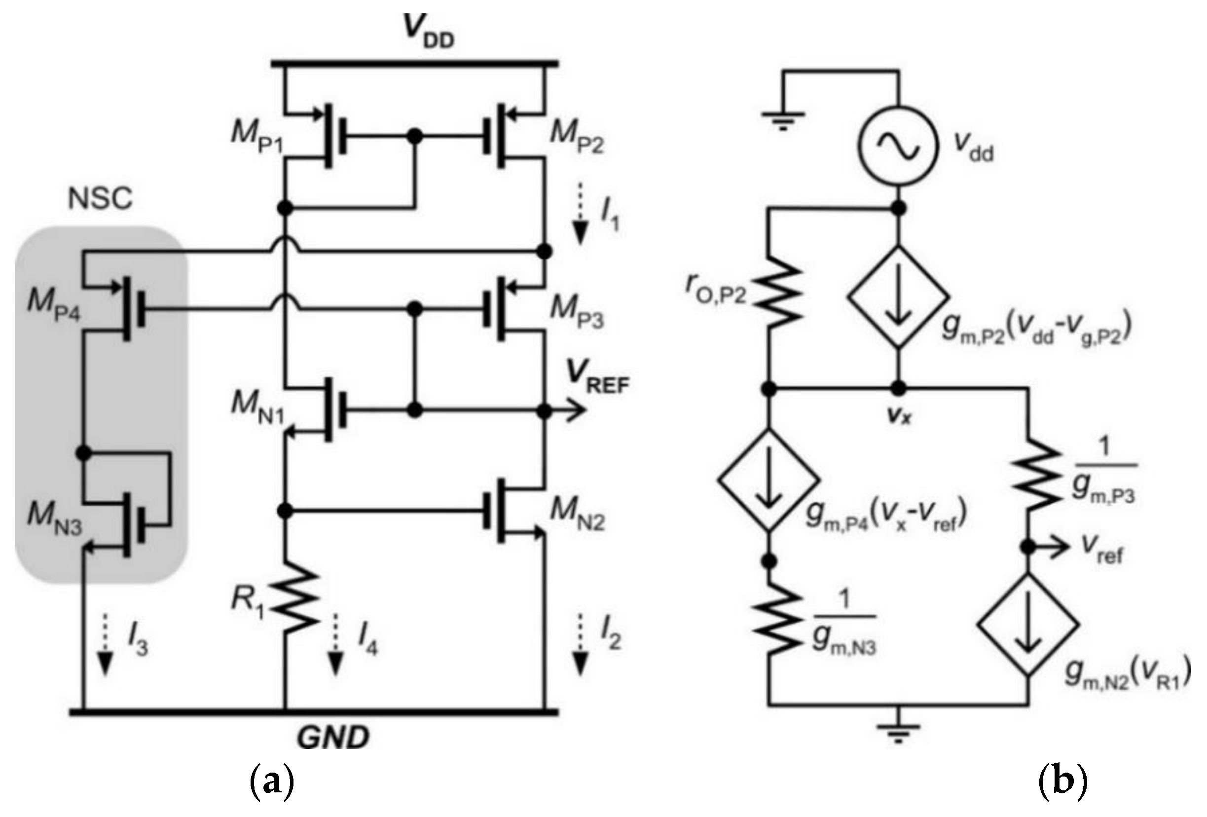
2.1. Static Analysis

The newly proposed circuit and its small-signal equivalent circuit are illustrated in Figure 2a,b respectively. The proposed circuit is based on a VGS reference supply independent current-reference circuit [13]. The loop around MN1 and MN2 has negative feedback; consequently, the output voltage at node VREF is unchanged even when the voltage across the resistor R1 varies. However, the nonlinear current I1 in the current mirror, produced by the square-low behavior of the transistor and channel length modulation that results in a nonzero slope for ID/VDS, deteriorates the DC level of the reference voltage. The second-order factor in the reference voltage due to the nonlinear current can be eliminated if a linear current flows into MP3. Therefore, the NSC formed by transistors MP4 and MN3 is proposed in Figure 2a, whereby a linear current can be produced in the output path. The slope of the output voltage with respect to VDD is also controlled by the NSC. As a result, improvements have been made in terms of its supply dependency and ripple rejection performance.
If I4 and VREF are constant, the gate–source voltages of MN1 and MN2 will also be constant. VREF can be expressed as follows:
V R E F = V G S , N 1 + V G S , N 2 .
A supply-independent reference voltage can be achieved if:
V R E F V D D = 0
or
V G S , N 1 V D D + V G S , N 2 V D D = 0
The gate–source voltage of MN1 can be obtained by first allowing the current in MN1 to saturate; hence,
I 4 = 1 2 k n , N 1 ( V G S , N 1 V T H , N 1 ) 2 ( 1 + λ N 1 V D S , N 1 ) .
Rearranging Equation (4) gives:
V G S , N 1 = 2 I 4 K n , N 1 · 1 ( 1 + λ N 1 V D S , N 1 ) 1 2 + V T H , N 1
and taking the derivative of VGS,N1 with respect to VDS,N1 results in:
V G S , N 1 V D S , N 1 = 2 I 4 K n , N 1 · λ N 1 2 ( 1 + λ N 1 V D S , N 1 ) .
By approximating V D S , N 1 V D D = 1 , we obtain, from Equation (6),
V G S , N 1 V D S , N 1 = V G S , N 1 V D D
From Figure 2a, we know that:
I 2 = I 1 I 3 .
The NSC senses the voltage variation at the source terminals of MP3 and MP4 by assuming that VREF is constant and that the nonlinear current in I1 sinks into MP4 leaving a linear current in MP3. By assuming that I1 and I3 grow linearly with respect to VDD, we can rewrite I2 in Equation (8) as follows:
I 2 = m 1 V D D + C 1 ( m 3 V D D + C 3 ) = V D D ( m 1 m 3 ) + ( C 1 C 3 ) ,
where m1 and m3 are the slopes of I1 and I3, respectively, and C1 and C3 are constant values. I2 can also be written as:
I 2 = 1 2 k n , N 2 ( V G S , N 2 V T H , N 2 ) 2 .
By substituting Equation (9) into (10), Equation (10) becomes:
V D D ( m 1 m 3 ) + ( C 1 C 3 ) = 1 2 k n , N 2 ( V G S , N 2 V T H , N 2 ) 2 .
Rearranging Equation (11) for VGS,N2 gives:
V G S , N 2 = 2 K n , N 2 . ( m 1 m 3 ) V D D + ( C 1 C 3 ) + V T H , N 2
and taking the derivative of VGS,N2 with respect to VDD results in:
V G S , N 2 V D D = 2 K n , N 2 · ( m 1 m 3 ) 2 ( m 1 m 3 ) V D D + ( C 1 C 3 ) .
Substituting Equations (6) and (13) into (3) produces:
2 I 4 K n , N 1 · λ N 1 2 ( 1 + λ N 1 V D S , N 1 ) + 2 K n , N 2 · ( m 1 m 3 ) 2 ( m 1 m 3 ) V D D + ( C 1 C 3 ) = 0 .
A key parameter of interest in Equation (14) is m3. To satisfy the condition in Equation (2), m3 in Equation (14) can be controlled by adjusting the size of transistor MP4. The slope of m3 should be less than m1, so that the first term of Equation (14) can be subtracted to zero. Trimming the transistor’s width and length can be performed by the Cadence Spectre simulation to optimize the output voltage variation.

2.2. Dynamic Analysis

The dynamic behavior of the proposed circuit can be determined by analyzing the equivalent circuit shown in Figure 2b. MN1 and R1 form a source follower. For simplifying the design equations, we presume that g m , N 1 R 1 1 ; as a result, vR1 is close to vref and vg,p2 can be approximately equal to vdd. From Figure 2b, by applying Kirchhoff’s current law at node vx, we can derive the following equation:
v d d v x r o , P 2 = g m , P 4 v x + v r e f ( g m , N 2 g m , P 4 ) .
vx can be derived from the circuit given as:
v x = v r e f ( g m , N 2 + g m , P 3 g m , P 3 )
By substituting Equation (16) into (15), the ratio of vref to vdd can be obtained as follows:
v r e f v d d g m , P 3 r o , P 2 ( g m , N 2 × g m , P 4 + g m , N 2 × g m , P 3 )
Accordingly, Equation (17) shows that vref becomes decoupled from small variations in vdd when the output resistance of ro,P2 is sufficiently high. The NSC produces the g m , P 4 in the denominator of Equation (17), which can help improve the PSRR performance.
Table 1 shows all the parameters used in the proposed reference circuit in Figure 2b.

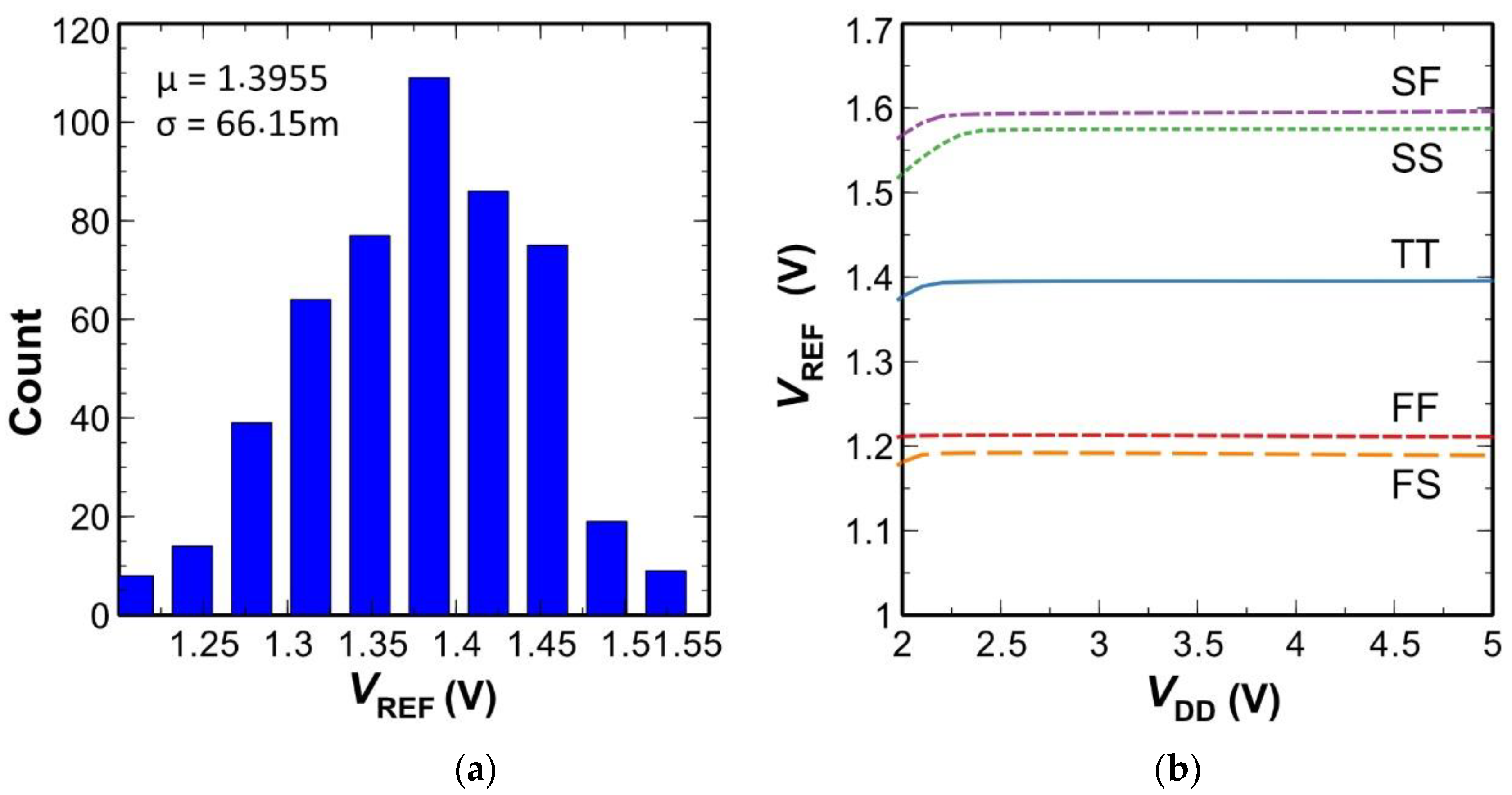
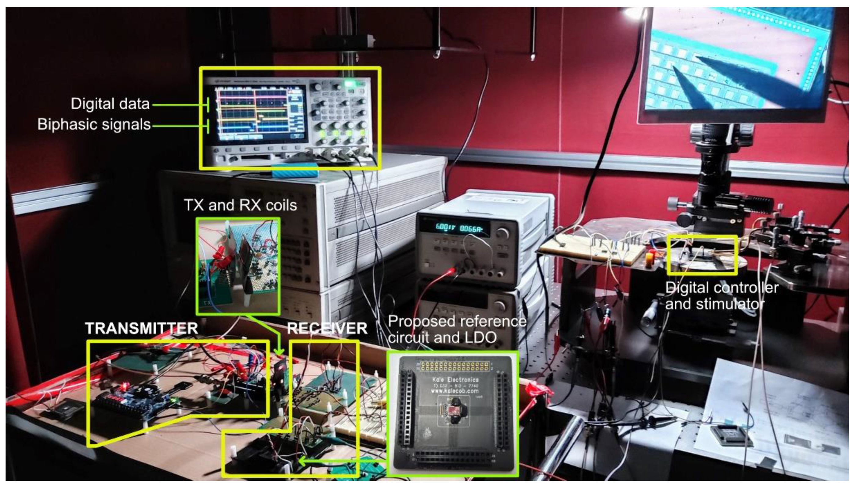
3. Simulation and Measurement Results

The proposed supply independent voltage reference circuit was fabricated using SK Hynix 0.35 µm CMOS technology. The micrograph of the proposed reference circuit is displayed in Figure 3a, and it occupies an active area of 0.0131 mm2. Figure 3b illustrates the transient response of the output voltage VREF when VDD is ramped from 0 to 5 V. When the current starts flowing in the circuit, the self-biasing reference circuit drives itself towards the desired stable state, according to the measurement, the output voltage starts settling at 1.37 V when VDD reaches over 2 V.
The measured output voltage variation with respect to VDD is plotted in Figure 4a. The inset graphs show the measured and simulated results when VDD varies from 2 V to 5 V and 0 to 30 V, respectively. The observed output voltage increases linearly by 10 mV for VDD variation from 2.1 V to 5 V. This results in a line regulation of 3.45 mV/V. This dependency can be further optimized by adjusting MP4, as indicated in Equation (14). The simulation shows a stable reference voltage even when VDD reaches up to 30 V. However, the measurement was stopped by the breakdown voltage of ~6 V for transistors. The variation of VREF between 2.4 V to 30 V for VDD is only 11 mV, which results in a line regulation of 0.4 mV/V. The measured and simulated PSRR of the proposed reference circuit is displayed in Figure 4b, where we obtain the simulated PSRR of −67 dB without the NSC block and −112 dB with one, respectively. This shows that the nonlinear current sink circuit we proposed in this work works as expected. In reality, however, a maximum PSRR of −93 dB is observed for frequencies lower than 1 kHz. The difference of −19 dB between the simulation and measurement is probably due to the parasitic capacitance that arises from the metal lines and pads in the fabricated chip, where our proposed reference circuit shares the power supply rails of other test blocks.
Figure 5a illustrates 500 Monte Carlo simulation results of the reference voltage. The average reference voltage, μ, and the standard deviation, σ, are 1.3955 V and 66.15 m, respectively. The line regulation results in different corners are shown in Figure 5b. The results indicate that the effectiveness of NSC produces stable reference voltage in all corners. The worst case occurs in SS condition in which the line regulation of 34.4 mV/V is obtained for VDD variation from 2.1 V to 5 V.
The overall electrical performance of the CMOS reference circuit designed in this work is summarized in Table 2, where it is also compared with the performances of the prior designs presented in [14,15,16,17].
To verify the real performance of the proposed reference circuit, we applied it to the low-voltage-drop regulator (LDO) circuit plotted in Figure 6a. This LDO circuit that utilizes an output ringing compensation circuit was fabricated in the same chip displayed in Figure 3a. The output of the LDO provides a positive supply voltage to 64 pixels stimulator circuit which requires maximum current of 10 mA. This requirement is based on our previous work which can be found in [10]. In the experimental setup to evaluate the line-transient responses of LDO, a 100 Ω resistor was chosen as a load for the LDO output terminal so that the load current is larger than 10 mA. When we applied a ramp voltage varying from 0 to 5 V, the LDO still output a constant voltage of 1.62 V, as shown in Figure 6b, while the reference circuit output 1.37 V. While maintaining a load current of 16.2 mA, the LDO output variation was observed as 17.6 mV in the supply range from 2.5 V to 5 V. The overshoot and undershoot voltages were 80 mV and 100 mV, respectively, as illustrated in Figure 6c. This LDO also had a fast recovery time of 240 ns, corresponding to the rapid change of VDD from 5 V to 5.2 V in 20 ns. Presently, we evaluated the full-path system using separate chips for LDO, digital controller and stimulator shown in Figure 7.
In the near future, the proposed voltage-reference circuit working with the LDO can be applied to fully integrated retinal prosthetic systems. Our proved concept prototype system could be further miniaturized and potentially transformed into stretchable devices which is beyond the flatland constrain of the traditional wafer-based system. Currently, we have developed a stretchable receiving coil and are progressively working on flexible microelectrode arrays.

4. Conclusions

In this paper, a novel CMOS voltage-reference circuit with high PSRR and wide-range supply independence was proposed and designed for a subretinal prosthetic system. The proposed NSC reduced the supply ripples significantly and sank out undesired signals in the reference voltage. Experimental results exhibited good agreement with the proposed concept and demonstrated better performance in supply independence and PSRR, when compared to the previous works. The proposed circuit provided a constant output voltage of 1.37 V and exhibited 10 mV variations over the supply range from 2.1 V to 5 V, resulting in a line regulation of 3.45 mV/V. The maximum PSRR was observed to be −93 dB for frequencies below 1 kHz. The current proof-of-concept prototype was implemented on a single chip with the LDO circuit, using a standard 0.35 µm CMOS process. The proposed reference design occupied an active area of 0.0131 mm2. Considering the high precision and small size design, this novel reference circuit can be used for implantable devices such as retinal prostheses and cochlear implants. As a future work, we will integrate the proposed reference circuit and LDO onto a single chip along with other functional blocks such as a demodulator, digital control, and high-density stimulator array.

Author Contributions

Conceptualization, R.B.A.Z., and J.K.; methodology, R.B.A.Z. and J.K.; formal analysis, R.B.A.Z., H.C., and J.K.; writing—original draft preparation, R.B.A.Z., H.C., and J.K.; writing—review and editing, R.B.A.Z., H.C., and J.K.; supervision, H.C., and J.K.; project administration, J.K.; funding acquisition, J.K. All authors have read and agreed to the published version of the manuscript.

Funding

This research was partially supported by the National Research Foundation of Korea (Grant No. NRF-2017M3A9E2056461) and the Gachon University Research Fund (2018-0324). This work was supported by the National Research Foundation of Korea grant funded by the government (MSIT) (No. 2020R1A2C4001606).

Acknowledgments

The authors would like to express their sincerest appreciation to the IC Design Education Center for chip fabrication.

Conflicts of Interest

The authors declare no conflict of interest.

References

  1. Lee, B.; Kiani, M.; Ghovanloo, M. A Triple-Loop Inductive Power Transmission System for Biomedical Applications. IEEE Trans. Biomed. Circuits Syst. 2016, 10, 138–148. [Google Scholar] [CrossRef] [PubMed]
  2. Jegadeesan, R.; Nag, S.; Agarwal, K.; Member, S. Enabling Wireless Powering and Telemetry for Peripheral Nerve Implants. IEEE J. Biomed. Health Inform. 2015, 19, 958–970. [Google Scholar] [CrossRef] [PubMed]
  3. Lo, Y.-K.; Chen, K.; Gad, P.; Liu, W. An On-Chip Multi-Voltage Power Converter with Leakage Current Prevention Using 0.18 um High-Voltage CMOS Process. IEEE Trans. Biomed. Circuits Syst. 2016, 10, 163–174. [Google Scholar] [CrossRef] [PubMed]
  4. Ha, S.; Khraiche, M.L.; Akinin, A.; Jing, Y.; Damle, S.; Kuang, Y.; Bauchner, S.; Lo, Y.-H.; Freeman, W.R.; Silva, G.A.; et al. Towards high-resolution retinal prostheses with direct optical addressing and inductive telemetry. J. Neural Eng. 2016, 13, 056008. [Google Scholar] [CrossRef] [PubMed]
  5. Goetz, G.A.; Palanker, D.V. Electronic approaches to restoration of sight. Rep. Prog. Phys. 2016, 79, 096701. [Google Scholar] [CrossRef] [PubMed] [Green Version]
  6. Lin, T.-C.; Chang, H.-M.; Hsu, C.-C.; Hung, K.-H.; Chen, Y.-T.; Chen, S.-Y.; Chen, S.-J. Retinal prostheses in degenerative retinal diseases. J. Chin. Med. Assoc. 2015, 78, 501–505. [Google Scholar] [CrossRef] [PubMed] [Green Version]
  7. Wu, C.-Y.; Tseng, C.-K.; Liao, J.-H.; Chiao, C.-C.; Chu, F.-L.; Tsai, Y.-C.; Ohta, J.; Noda, T. CMOS 256-Pixel/480-Pixel Photovoltaic-Powered Subretinal Prosthetic Chips with Wide Image Dynamic Range and Bi/Four-Directional Sharing Electrodes and Their Ex Vivo Experimental Validations With Mice. IEEE Trans. Circuits Syst. I Regul. Pap. 2020, 67, 3273–3283. [Google Scholar] [CrossRef]
  8. Kuo, P.H.; Wong, O.-Y.; Tzeng, C.-K.; Wu, P.-W.; Chiao, C.C.; Chen, P.-H.; Tsai, Y.-C.; Chu, F.-L.; Ohta, J.; Tokuda, T.; et al. Improved Charge Pump Design and Ex Vivo Experimental Validation of CMOS 256-Pixel Photovoltaic-Powered Subretinal Prosthetic Chip. IEEE Trans. Biomed. Eng. 2020, 67, 1490–1504. [Google Scholar] [CrossRef] [PubMed]
  9. Özmert, E.; Arslan, U. Retinal Prostheses and Artificial Vision. Turk. J. Ophthalmol. 2019, 49, 213–219. [Google Scholar] [CrossRef] [PubMed]
  10. Kang, H.; Abbasi, W.H.; Kim, S.-W.; Kim, J. Fully Integrated Light-Sensing Stimulator Design for Subretinal Implants. Sensors 2019, 19, 536. [Google Scholar] [CrossRef] [PubMed] [Green Version]
  11. Kim, J.; Basham, E.; Pedrotti, K.D. Geometry-based optimization of radio-frequency coils for powering neuroprosthetic implants. Med. Biol. Eng. Comput. 2013, 123–134. [Google Scholar] [CrossRef] [PubMed]
  12. Zawawi, R.B.A.; Abbasi, W.H.; Kim, S.-H.; Choi, H.; Kim, J. Wide-Supply-Voltage-Range CMOS Bandgap Reference for In Vivo Wireless Power Telemetry. Energies 2020, 13, 2986. [Google Scholar] [CrossRef]
  13. Gray, P.; Meyer, R. Analysis and Design of Analog Integrated Circuits, 5th ed.; John Wiley and Sons: Hoboken, NJ, USA, 2010. [Google Scholar]
  14. Zhou, Z.-K.; Shi, Y.; Wang, Y.; Li, N.; Xiao, Z.; Wang, Y.; Liu, X.; Wang, Z.; Zhang, B. A Resistorless High-Precision Compensated CMOS Bandgap Voltage Reference. IEEE Trans. Circuits Syst. I Regul. Pap. 2019, 66, 428–437. [Google Scholar] [CrossRef]
  15. Chi-Wa, U.; Zeng, W.-L.; Law, M.-K.; Lam, C.-S.; Martins, R.P. A 0.5-V Supply, 36 nW Bandgap Reference With 42 ppm/°C Average Temperature Coefficient Within −40 °C to 120 °C. IEEE Trans. Circuits Syst. I Regul. Pap. 2020, 67, 3656–3669. [Google Scholar]
  16. Kim, M.; Cho, S.H. A 0.0082-mm&sup2, 192-nW Single BJT Branch Bandgap Reference in 0.18-μm CMOS. IEEE Solid State Circuits Lett. 2020, 3, 426–429. [Google Scholar]
  17. Sodagar, A.; Najafi, K. A wide-range supply-independent CMOS voltage reference for telemetry-powering applications. In Proceedings of the 9th International Conference on Electronics, Circuits and Systems, Dubrovnik, Croatia, 15–18 September 2002; Institute of Electrical and Electronics Engineers (IEEE): Piscataway, NJ, USA, 2003; Volume 1, pp. 401–404. [Google Scholar]
Figure 1. Retinal prosthetic system architecture.
Electronics 09 02028 g001
Figure 2. (a) Proposed reference circuit and (b) its small-signal equivalent circuit.
Electronics 09 02028 g002
Figure 3. (a) Micrograph of the proposed reference circuit, (b) measured transient response.
Electronics 09 02028 g003
Figure 4. Measured results of (a) line regulation and (b) power supply rejection ratio (PSRR).
Electronics 09 02028 g004
Figure 5. (a) 500 Monte Carlo simulation results at 3.3 V supply, 27 °C; (b) line regulation results in different corners.
Electronics 09 02028 g005
Figure 6. (a) Low-voltage-drop regulator (LDO) circuit incorporating the proposed reference circuit; (b) measured line-transient responses; and (c) measured overshoot and undershoot voltages.
Electronics 09 02028 g006
Figure 7. Full-path prosthetic system experimental setup.
Electronics 09 02028 g007
Table 1. Component parameters.
ComponentParameterComponentParameter
MP1, MP2W = 4 µm, L = 1 µm, m = 50MN2W = 25 µm, L = 3 µm, m = 4
MP3W = 1.15 µm, L = 1 µm, m = 1MN3W = 4 µm, L = 1 µm, m = 20
MP4W = 4 µm, L = 1 µm, m = 9R170 kΩ
MN1W = 4 µm, L = 1 µm, m = 10
Table 2. Electrical performance summary and comparison of reference circuit with previous designs.
Parameter[14][15][16][17]This Work
Supply voltage range (V)2 to 50.5 to 11.3 to 1.82.6 to 12
(2.4 to 20) *
2.1 to 5
(2.4 to 30) *
Reference output voltage (V)1.140550.4951.171.61.37
Line regulation (mV/V)23.20.350.957
(0.511) *
3.45
(0.39) *
PSRR (dB)−61−50−52−60
(−59.2) *
−93
(−112) *
Chip Area (mm2)0.03960.05220.082-0.0131
Technology (µm)0.350.0650.181.60.35
* Simulation result.
Publisher’s Note: MDPI stays neutral with regard to jurisdictional claims in published maps and institutional affiliations.

