Abstract
A high-slew-rate, low-power, CMOS, rail-to-rail buffer amplifier for large flat-panel-display (FPD) applications is proposed. The major circuit of the output buffer is a rail-to-rail, folded-cascode, class-AB amplifier which can control the tail current source using a compact, novel, adaptive biasing scheme. The proposed output buffer amplifier enhances the slew rate throughout the entire rail-to-rail input signal range. To obtain a high slew rate and low power consumption without increasing the static current, the tail current source of the adaptive biasing generates extra current during the transition time of the output buffer amplifier. A column driver IC incorporating the proposed buffer amplifier was fabricated in a 1.6-μm 18-V CMOS technology, whose evaluation results indicated that the static current was reduced by up to 39.2% when providing an identical settling time. The proposed amplifier also achieved up to 49.1% (90% falling) and 19.9 % (99.9% falling) improvements in terms of settling time for almost the same static current drawn and active area occupied.
1. Introduction
The demand for large, high-resolution flat-panel-display (FPD) panels has strong requirements for low-power, high-slew-rate operation for thin-film transistor liquid-crystal display (TFT-LCD) column (data or source) drivers. As display panels need to be larger and have higher resolution, the column drivers of an LCD driving system are becoming important to drive more efficiently large resistive and capacitive loads with low-power dissipation, small area and fast settling time. A column driver of a FPD panel generally includes shift registers, input registers, data latches, level shifters, digital-to-analog converters (DACs) and output buffers with output switches [1,2,3,4,5,6,7,8,9,10]. FPD driving systems generally use analog [11,12,13,14,15,16,17,18,19] or digital driving methods [20,21]. As the display resolution increases, the resistance and capacitance loads of the output buffer increase, whereas the required settling time decreases. The target settling time of the output buffer for the LCD column drivers should be shorter than the horizontal scanning time of the panel [11,12,14,15,16,17,18,19]. Rail-to-rail class-A, AB or B amplifiers described in [11,12,13,14,15,16,17,18,19] have been generally used as buffer amplifiers of FPD column drivers. The output buffer amplifier in [11] is used a rail-to-rail input stage and a dual-path push-pull output stage with both class-B and class-AB output sections combined together to improve slew rate. Based on the traditional design in [13], the buffer amplifier in [16] uses several rail-to-rail input stages for 4-bit or 3-bit voltage interpolation with gm-modulation. When used as an output buffer amplifier, its operation is the same as that of the buffer amplifier in [13] because several input stages collectively operate as one. The output buffer amplifier in [17] has the same structure as the buffer amplifier in [13], except that explicit output-polarity multiplexer switches are incorporated to improve settling time, and a single differential pair is used as the input stage of the buffer. The output buffer amplifier in [15] was adopted to implement an area-efficient 10-bit DAC by a buffer-reusing method when a large transient driving capability, small static current and compact layout area were required. These buffer amplifiers have their output slew rate proportional to the input bias current. Therefore, the static power consumption increases as the bias current is increased to provide a high-slew-rate performance. To enhance the slew rate without a large static bias current, rail-to-rail, folded-cascode, class-AB buffer amplifiers with dynamic biasing have been proposed [18,19]. However, they have some drawbacks. In [18], the dynamic biasing circuit uses a P-type slew detector for increasing the tail current of the N-type input differential pair of the core amplifier, and uses an N-type slew detector for increasing the tail current of the P-type input differential pair. Consequently, the slew rate can be enhanced, but power and area overheads also become higher. Moreover, since an opposite type of slew detector is used for each input differential pair, the buffer amplifier cannot be fully functional for the entire rail-to-rail input signal range. To address this problem, a modified class-AB output amplifier shown in Figure 1 was proposed [19]. In this buffer amplifier, the dynamic biasing circuit has been modified to allow the same types of slew detectors as the input differential pairs to be used for dynamically adjusting the bias current, resulting in a full slew rate enhancement throughout the entire rail-to-rail signal range. However, unfortunately, the resulting dynamic biasing circuit requires many transistors (as much as 26 transistors). Thus, like [18], it still causes substantially increased power and area overheads. Consequently, a high-slew-rate output buffer amplifier with low-power consumption and a small area is indispensable for the design of TFT-LCD column drivers.
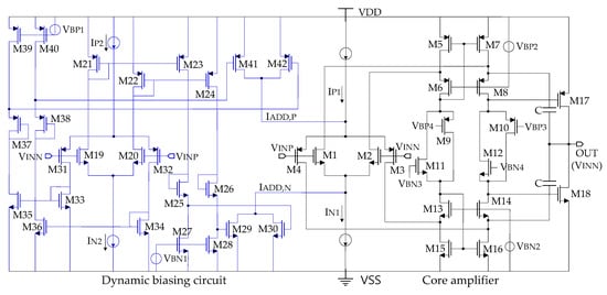
Figure 1.
Conventional buffer amplifier with slew rate enhancement for an entire rail-to-rail input and output signal range [19].
To address these issues, a high-slew-rate, low-power, rail-to-rail, folded-cascode, class-AB output buffer amplifier with compact adaptive biasing is proposed in this paper. We present a newly developed output buffer amplifier that requires substantially smaller overheads in terms of power and area to provide an increased slew rate capability. The rest of the paper is arranged as follows. In Section 2, the structure and operation of the proposed buffer amplifier is described with discussion on the advantages of the proposed circuit. In Section 3, evaluation and comparison results are presented based on experimental data measured from a column driver IC incorporating the proposed buffer amplifier. Finally, conclusions are given in Section 4.
2. Proposed Buffer Amplifier
The circuit schematic of the proposed buffer amplifier is shown in Figure 2. It is configured as a complementary differential input stage followed by a floating current source stage for providing a rail-to-rail input common-mode range with class-AB operation as conventional buffer amplifiers do. However, unlike the conventional buffer amplifiers, the proposed buffer amplifier does not use a bulky dynamic biasing circuit having auxiliary differential pairs and multiple current mirrors for slew rate enhancement. Instead, it incorporates just two additional transistors, MP3A and MN3A, as tail current sources of the common source amplifier in the complementary input stage, which are driven by signals, Pu and Pd, driving output driver transistors, MP8 and MN8, respectively. Transistors MP9, MN9, MN10 and MN11 (MN12, MP10, MP11 and MP12) for the current mirror operation of MP3A (MN3A) are used for full slew rate enhancement throughout entire rail-to-rail signal range. MN9 (MN10) is used to reduce the static current by lowering the drain and gate voltage of the current mirror transistors, MN10 and MN11 (MP11 and MP12), and the static current of the common source amplifiers, while MP9 and MN12 act as additional tail current sources. Subsequently, the proposed buffer amplifier combines main tail current sources (MP3 and MN3) and auxiliary tail current sources (MP3A and MN3A) in the input stage for fast transient operation. These auxiliary transistors are sized to be about 40 times smaller than output drivers MP8 and MN8. Moreover, due to the narrow width effect [20], in which the threshold voltage of a MOS transistor is increasing as the transistor width becomes narrower, the threshold voltages of MP3A and MN3A become higher than those of MP8 and MN8 in the steady state. These effects are combined to let the bias currents in MP3A and MN3A be much smaller than those of MP8 and MN8. For example, in our design (DC 8.5 V = VDD/2 @VDD = 17 V), the sizes of MP3A and MN3A are such that the threshold voltages are made to be 937 and 964 mV, whereas the sizes of MP8 and MN8 are such that the threshold voltages are made to be 808 and 831 mV, respectively, resulting in about 130 mV higher threshold voltages for MP3A and MN3A than those of MP8 and MN8. Now, the bias voltages at Pu and Pd are set at VDD 888 and 910 mV, respectively, so that they are larger than the threshold voltages of MP8 and MN8 and less than those of MP3A and MN3A. This leads to a bias current of about 5 nA for MP3A and MN3A, which is negligible as compared to the bias currents of MP3/MN3 (1.6 µA), MP5/MN5 (2.1 µA), MP7/MN7 (2.1 µA) and MP8/MN8 (5.6 µA), resulting in almost no increase on overall bias current of the amplifier in the steady state.
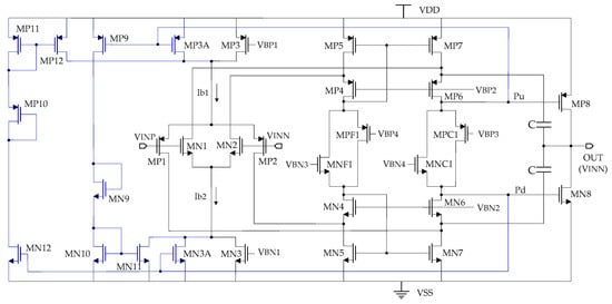
Figure 2.
Proposed buffer amplifier with area- and power-efficient slew rate enhancement throughout entire rail-to-rail signal range.
As for the operation principle, when the input has some voltage swing, the voltages at Pu and Pd go up or down depending on input polarity, so the gate-to-source voltages (VGS) of MP3A and MN3A increase or decrease accordingly. For a very large input voltage difference, the voltage of Pu (Pd) can change from its nominal value to near ground (VDD). Then, the amount of current flowing through MP3A (MN3A) increases substantially, resulting in a larger bias current in the input stage for slew rate enhancement only during the rising and falling transitions of the output buffer amplifier. When the input swing (VINP) is small, Pu and Pd have small voltage changes, so MP3A and MN3A have low current. In addition, when the input voltage swing becomes larger, Pu and Pd have large voltage excursions, so MP3A and MN3A draw a higher current, resulting in a faster transient response. The auxiliary adaptive tail current increases to obtain a faster transient response when the voltage of node Pu is low in the rising transition of the input (output) voltage swing, and the voltage of node Pd is high in the falling transition. The voltage of node Pu offers lower levels and the voltage of node Pd offers higher levels with the larger capacitive load and the voltage swing of the larger input transient. Therefore, the output buffer amplifier has a good driving capability when the capacitive load is larger and the voltage swing of the input transient response is higher.
The proposed buffer amplifier can provide a substantial slew rate enhancement during a full-swing transition for high voltage, as conventional buffer amplifiers do. However, as compared to the conventional high-slew-rate amplifiers in [18,19], the proposed buffer amplifier uses a significantly smaller number of transistors for embodying the slew rate enhancement and is fully functional for the entire rail-to-rail input signal range. Actually, the buffer amplifier in [18] requires 12 transistors to embody slew rate enhancement and is not fully functional for the entire input range. The buffer amplifier in [19] overcomes the input voltage range problem, but requires as much as 26 transistors to achieve high-slew-rate operation. Meanwhile, in the proposed buffer amplifier, just two additional transistors in the complementary differential input stage, which act as extra tail current sources, and eight transistors for configuring current mirrors, are used to provide high-slew-rate operation, resulting in a significant reduction in terms of silicon area and power consumption.
3. Experimental Results
A column driver IC incorporating the proposed buffer amplifier for a large-sized flat-panel-display (FPD) was designed and fabricated using a 1.6 μm 18 V CMOS technology. The layout picture of the column driver IC is depicted in Figure 3a, where the active area occupies 12,685 μm2 × 1010 μm2. Figure 3b shows that the measured output waveforms for the white pattern (full-swing) in the dot inversion prove a fast transient response of the proposed output buffer circuit. The simulated output waveforms of the conventional buffer amplifiers published in [13,19] and of the proposed buffer amplifier are shown in Figure 4, where the settling behavior can be compared. The conditions for the simulation were that the buffer amplifiers were identically driving a resistance of 8.5 ΚΩ and a capacitance of 300 pF as the column-line load of a 55-inch TFT-LCD panel at a voltage swing from 0.2 V to 16.8 V. As recognized by the Figure 4, the settling time for rising and falling transitions of the proposed output buffer is much faster than that of [13], and similar to that of [19]. Note that, for achieving this high performance, the proposed buffer amplifier uses far less static current than the conventional buffer amplifier in [19], as seen below (Table 1 and Table 2). The performance matric such as the static current, dynamic current, settling times and active area of the proposed buffer amplifier are summarized and compared with those of conventional buffer amplifiers based on experimental measurement results in Table 1. For some representative ones, the performance comparison in the same process technology is also shown in Table 2, where the simulated and measured data of the proposed buffer amplifier are well matched to each other. As indicated in Table 2, the static current of the proposed buffer amplifier in the 2·gm region of the input stage where the dc quiescent current consumes the most is reduced from 18.86 μA to 11.44 μA (39.3% reduction) as compared to [19] for providing a similar settling performance. As shown in Table 1 and Table 2, the output buffer in [11] has a slower 99.9% slew rate than the proposed buffer amplifier, although the capacitive load is large but the RC load is much smaller. The output buffer in [16] requires a driving voltage higher by 1 V (6%) but has a slower settling time than the proposed buffer amplifier, even though the resistive load is 3.5 ΚΩ (41.2%) smaller. The output buffer in [15] has a slower 99.9% settling time than the proposed buffer amplifier, although the RC load is much smaller and the driving voltage is lower. The output buffer in [17] has the same structure as the buffer amplifier in [13], except using output-polarity multiplexer switches and a single differential pair input stage. The buffer has a slower 90% settling time than the proposed buffer amplifier, although the RC load is smaller. As compared to [19], which has an adaptive biasing structure, the active area of the proposed buffer amplifier is reduced from 8401 to 4960 μm2 (40.9% reduction). As compared to [13], the proposed amplifier achieves up to 49.1% (90% falling) and 19.9% (99.9% falling) improvements in terms of settling time for almost the same static current drawn and active area occupied. The robustness of the proposed scheme against process and temperature variations is summarized in Table 3 using corner simulations at NN 25 °C, FF −30 °C and SS 125 °C. The improved performance of the proposed buffer amplifier comes from the fact that the buffer can achieve the slew rate enhancement much more efficiently using a smaller number of transistors, resulting in a higher area efficiency, lower power consumption and faster settling. The experimental evaluation results presented above imply that the proposed buffer amplifier is applicable to amplifiers with high-slew-rate operations and well suited as a column driver for large, high-definition FPDs.
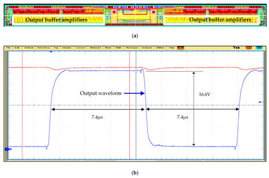
Figure 3.
A column driver IC using the proposed output buffer amplifier. (a) Layout picture and (b) measured output waveform of the white pattern (VSS2 +0.2 V (0.2 V)—VDD −0.2 V (16.8 V)) in the dot inversion.
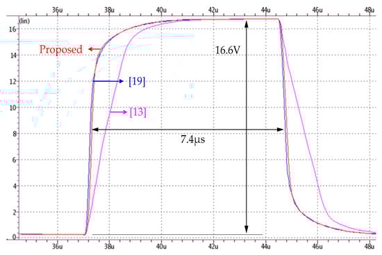
Figure 4.
Simulated output waveforms of buffer amplifiers.

Table 1.
Performance comparison of buffer amplifiers.
Table 2.
Performance comparison of buffer amplifiers with the same technology.
Table 3.
Corner simulation results for the proposed buffer amplifier (8.5 V @VDD = 17 V).
4. Conclusions
A high-speed, low-power, rail-to-rail, folded-cascode, class-AB output buffer amplifier with an adaptive biasing circuit is proposed. The proposed buffer amplifier uses a compact, novel, adaptive biasing scheme for a slew rate enhancement. To obtain a faster transient response, the proposed adaptive biasing scheme requires just two transistors of the additional tail current sources and eight transistors for current mirrors. These additional transistors can provide a significant amount of extra bias current to the core amplifier during the slewing period while consuming a negligible amount of current during the steady-state period. The proposed adaptive biasing method can be applicable to amplifiers for high-slew-rate operation, and is well suitable for column drivers in large, high-definition FPDs.
Author Contributions
Methodology, validation, investigation, writing and conceptualization, C.-H.A. funding acquisition, supervision, investigation, writing, reviewing and editing, B.-S.K. All authors have read and agreed to the published version of the manuscript.
Funding
This research received no external funding.
Acknowledgments
This work was supported by Magnachip semiconductor Inc. This work was also supported by the National Research Foundation of Korea (NRF) grant funded by the Korean Government (MSIT) (2019R1A2C1011155); by the MOTIE and KEIT (20010560, Development of system level design and verification for in-storage processing architecture based on phase change memory); by the National Research Foundation of Korea (NRF) grant funded by the Korea government (MIST) (2020M3H2A1076786); by the Institute of Information and Communications Technology Planning and Evaluation (IITP) grant funded by the Korean Government (MIST) (2019-0-00421, AI Graduate School Support Program (Sungkyunkwan University); and by the National Research Foundation of Korea (NRF) grant funded by the Korea government (MIST) (NRF-2020M3F3A2A01082301).
Conflicts of Interest
The authors declare no conflict of interest.
References
- Kim, J.-S.; Jeong, D.-K.; Kim, G. A multi-level multi-phase charge-recycling method for low-power AMLCD column drivers. IEEE J. Solid-State Circuits 2000, 35, 74–84. [Google Scholar] [CrossRef]
- Itakura, T.; Minamizaki, H.; Saito, T.; Kuroda, T. A 402-output TFT-LCD driver IC with power control based on the number of colors selected. IEEE J. Solid-State Circuits 2003, 38, 503–510. [Google Scholar] [CrossRef]
- Bell, M. An LCD column driver using a switch capacitor DAC. IEEE J. Solid-State Circuits 2005, 40, 2756–2765. [Google Scholar] [CrossRef]
- Lu, C.-W.; Huang, L.-C. A 10-Bit LCD Column Driver With Piecewise Linear Digital-to-Analog Converters. IEEE J. Solid-State Circuits 2008, 43, 371–378. [Google Scholar] [CrossRef]
- Lu, C.-W.; Shen, C.-C.; Chen, W.-C. An Area-Efficient Fully R-DAC-Based TFT-LCD Column Driver. IEEE Trans. Circuits Syst. I 2010, 57, 2588–2601. [Google Scholar] [CrossRef]
- Lu, C.-W.; Yin, P.-Y.; Lin, Y.-T. A Column Driver Architecture with Double Time-Division Multiplexing RDACs for TFT-LCD Applications. IEEE J. Solid-State Circuits 2014, 49, 2352–2364. [Google Scholar] [CrossRef]
- Lu, C.-W.; Huang, Y.-C.; Lin, Y.-S. Area-Efficient Fully R-DAC Based TFT-LCD Column Driver Architectures with DAC Sharing Techniques. J. Disp. Technol. 2015, 11, 689–697. [Google Scholar] [CrossRef]
- Yin, P.-Y.; Lu, C.-W.; Chen, Y.-H.; Liang, H.-C.; Tseng, S.-P. A 10-Bit Low-Power High-Color-Depth Column Driver with Two-Stage Multi-Channel RDACs for Small-Format TFT-LCD Driver ICs. J. Disp. Technol. 2015, 11, 1061–1068. [Google Scholar] [CrossRef]
- An, T.-J.; Hwang, M.-S.; Choe, W.-J.; Ahn, G.-C.; Lee, H.J. Area-Efficient Time-Shared Digital-to-Analog Converter with Dual Sampling for AMOLED Column Driver IC’s. IEEE Trans. Circuits Syst. I 2018, 65, 3227–3240. [Google Scholar] [CrossRef]
- Lu, C.-W.; Yin, P.-Y.; Lin, M.-Y. A 10-bit Two-Stage R-DAC with Isolating Source Followers for TFT-LCD and AMOLED Column-Driver ICs. IEEE Trans. VLSI Syst. 2019, 27, 326–336. [Google Scholar] [CrossRef]
- Grasso, A.D.; Palumbo, G.; Pennisi, S. Dual Push–Pull High-Speed Rail-to-Rail CMOS Buffer Amplifier for Flat-Panel Displays. IEEE Trans. Circuits Syst. II Express Briefs 2018, 65, 1879–1883. [Google Scholar] [CrossRef]
- Lu, C.-W.; Hsu, K.-J. A high-speed low-power rail-to-rail column driver for AMLCD application. IEEE J. Solid-State Circuits 2004, 39, 1313–1320. [Google Scholar] [CrossRef]
- Hogervorst, R.; Tero, J.; Eschauzier, R.; Huijsing, J. A compact power-efficient 3V CMOS rail-to-rail input/output operational amplifier for VLSI cell libraries. IEEE J. Solid-State Circuits 1994, 29, 1505–1513. [Google Scholar] [CrossRef]
- Ito, R.; Itakura, T.; Minamizaki, H. A Class AB amplifier for LCD driver. In Proceedings of the IEEE Symp. on VLSI Circuits, Kyoto, Japan, 14–16 June 2007; pp. 148–149. [Google Scholar]
- Xia, M.; Huang, Z.; Tian, L.; Wang, N.; Zhu, Y.; Wang, H.; Feng, S. An Area-Efficient 10-Bit Buffer-Reused DAC for AMOLED Column Driver ICs. Electronics 2020, 9, 208. [Google Scholar] [CrossRef]
- Lu, C.-W.; Lee, P.-Y.L.; Chang, Y.-G.; Huang, X.-W.; Cheng, J.-S.; Tseng, P.-Y.; Chou, C.-H.; Chen, P.; Chang, T.-Y.; Liu, J.Y.-C. A 10-bit 1026-Channel Column Driver IC With Partially Segmented Piecewise Linear Digital-to-Analog Converters for UHD TFT-LCDs with One Billion Color Display. IEEE J. Solid-State Circuits 2019, 54, 2703–2716. [Google Scholar] [CrossRef]
- An, C.-H.; Kim, H.-R.; Ko, J.-H.; Kong, B.-S. High-speed column-line driving with polarity switch-embedded output buffer amplifiers for TFT-LCD application. Electron. Lett. 2015, 51, 18–20. [Google Scholar] [CrossRef]
- Choi, J.; Min, K.; Yoo, C. High-Speed and Low-Power Analog Source Driver for TFT-LCD Using Dynamic Current Biased Operational Amplifier. SID Symp. Dig. Tech. Pap. 2007, 38, 1647–1650. [Google Scholar] [CrossRef]
- Kim, J.; Lee, J.; Choi, B. Slew-rate-enhanced rail-to-rail buffer amplifier for TFT LCD data drivers. Electron. Lett. 2012, 48, 924–925. [Google Scholar] [CrossRef]
- An, H.-K.; Zemanian, A. Computationally efficient determination of threshold voltages in narrow-channel MOSFET’s including fringing and inversion effects. IEEE Trans. Electron. Devices 1989, 36, 534–541. [Google Scholar] [CrossRef]
- Tai, Y.-H.; Lin, C.-H.; Ho, T.-H.; Huang, Y.-S.; Huang, S.-M.; Cho, W.-M. Fully Digital Driving Circuit for TFT LCD Using the Concept of Ramp-Stop. IEEE Trans. Ind. Electron. 2019, 66, 2074–2080. [Google Scholar] [CrossRef]
Publisher’s Note: MDPI stays neutral with regard to jurisdictional claims in published maps and institutional affiliations. |
© 2020 by the authors. Licensee MDPI, Basel, Switzerland. This article is an open access article distributed under the terms and conditions of the Creative Commons Attribution (CC BY) license (http://creativecommons.org/licenses/by/4.0/).