1. Introduction
Shunt active power filters (SAPFs) improve the power quality and energy efficiency in electrical systems by compensating the effects of unbalanced currents, reactive power, and harmonic distortion produced by inefficient loads [
1,
2]. The SAPF measures load currents and grid voltages at the point of common coupling (pcc) and then generates the inefficient currents required by the load, as shown in
Figure 1. In this way, the grid provides only useful power, improving power quality and energy efficiency of the grid.
SAPF current control methods can be classified into two groups: (i) linear designs based on small-signal models of the SAPF, and (ii) nonlinear designs base on large-signal models of the SAPF. Linear controllers are based on the application of linear control theory to linearized SAPF models. In this way, [
3,
4,
5,
6,
7] propose the use of proportional (P) controllers, proportional–integral (PI) controllers, and linear quadratic Gaussian (LQG) regulators, all working in a synchronous reference frame. In [
3,
8] the use of proportional resonant (PR) controllers is proposed. In [
9], the use of an
robust control design technique together with a Kalman filter for state estimation is proposed. In [
10,
11], a minimum time deadbeat control is proposed. Finally, [
12] proposes the application of model predictive control (MPC) together with a modulation algorithm to improve the current ripple.
As a result of the linearization of SAPF models, the control may degrade when the SAPF is not working close to the linearization point. Although the design of robust controllers might guarantee the stability for the whole operating range of the SAPF, it comes at the cost of performance degradation.
Some nonlinear controllers applied to the SAPF are the following: hysteresis band current control (HCC) [
13,
14,
15,
16,
17], sigma-delta control (SDC) [
18,
19], sliding mode control (SMC) [
20,
21,
22], and one-cycle control (OCC) [
23,
24,
25,
26,
27,
28].
The great advantage of HCC is its implementation simplicity and its good dynamic response; however, the variable switching frequency is its main drawback. In order to alleviate this problem, in [
15,
16,
17], changing the hysteresis band width dynamically (i.e., adjustable hysteresis band) is proposed, so as to obtain a quasi-fixed switching frequency.
SDC operation is asynchronous, hence, it suffers from the same drawbacks as HCC. In order to obtain synchronous sigma-delta control (SSDC), either an external clock signal is added to the sigma-delta modulator [
19], or an adjustable hysteresis band (AHB) is used in the comparator of the sigma-delta modulator [
18]. However, in [
19], although the switching frequency is bounded by the external clock, it is not fixed because it may be the case that when switching happens, the integral error has not reached the hysteresis bound yet. In the case of using an AHB, as in [
18], a fixed switching frequency can be obtained but at the cost of variable performance, because the current ripple depends on the hysteresis band, which is adjusted accordingly to keep the switching frequency fixed.
The HCC and SDC may be treated as special cases of SMC. SMC defines a sliding surface that characterizes the desired system performance, and a switched control that maintains the system on the surface. SMC is a well-developed theory with stable and robust results for general nonlinear control systems. However, as previously discussed, the design of SMC through HCC [
20] and SDC results in controllers that can guarantee constant switching frequency or fixed system performance, but not both.
Finally, OCC guarantees that, for each switching cycle, the duty cycle is adjusted to accomplish some control objective. In [
27], the duty cycle is computed to compensate the reactive power and harmonic distortion of load currents for single-phase and three-phase APFs. In [
25], OCC is applied to a three-phase APF system operating with asymmetrical grid voltages and a load demanding unbalanced and nonlinear currents; and in [
26], OCC is used in a three-phase four-leg APF to compensate the unbalanced, reactive and harmonic components of the load currents. Finally, OCC is used to compensate only for the load current harmonic components [
23,
24].
In this work, a new SAPF current control designed on the basis of the OCC paradigm is proposed. This control is based on the minimization of the integral error of the current on each switching period. Hence, the proposed control provides, with fixed switching frequency, a constant performance level of zero current integral error for each switching cycle. The influence of the switching pattern in the controller stability has also been studied. As a result, an alternating switching pattern strategy is selected to achieve stable behavior of the controller independently of the grid voltage sign. Implementation of this controller requires accurate measurements and high-speed computing to calculate the next switching period control in time. A real setup has been developed using a powerful microcontroller performing high-speed computing, combined with sigma-delta modulators to obtain precise measures at high sampling frequencies.
The paper is structured as follows. In
Section 2, the current control application is presented. In
Section 3, the proposed controller is derived, and the stability analysis is presented.
Section 4 presents stability analysis considering different switching patterns and the final control algorithm. In
Section 5, the control algorithm is tested under simulation.
Section 6 shows the experimental setup and the obtained results. Finally,
Section 7 includes the conclusions of the work.
2. Problem Statement
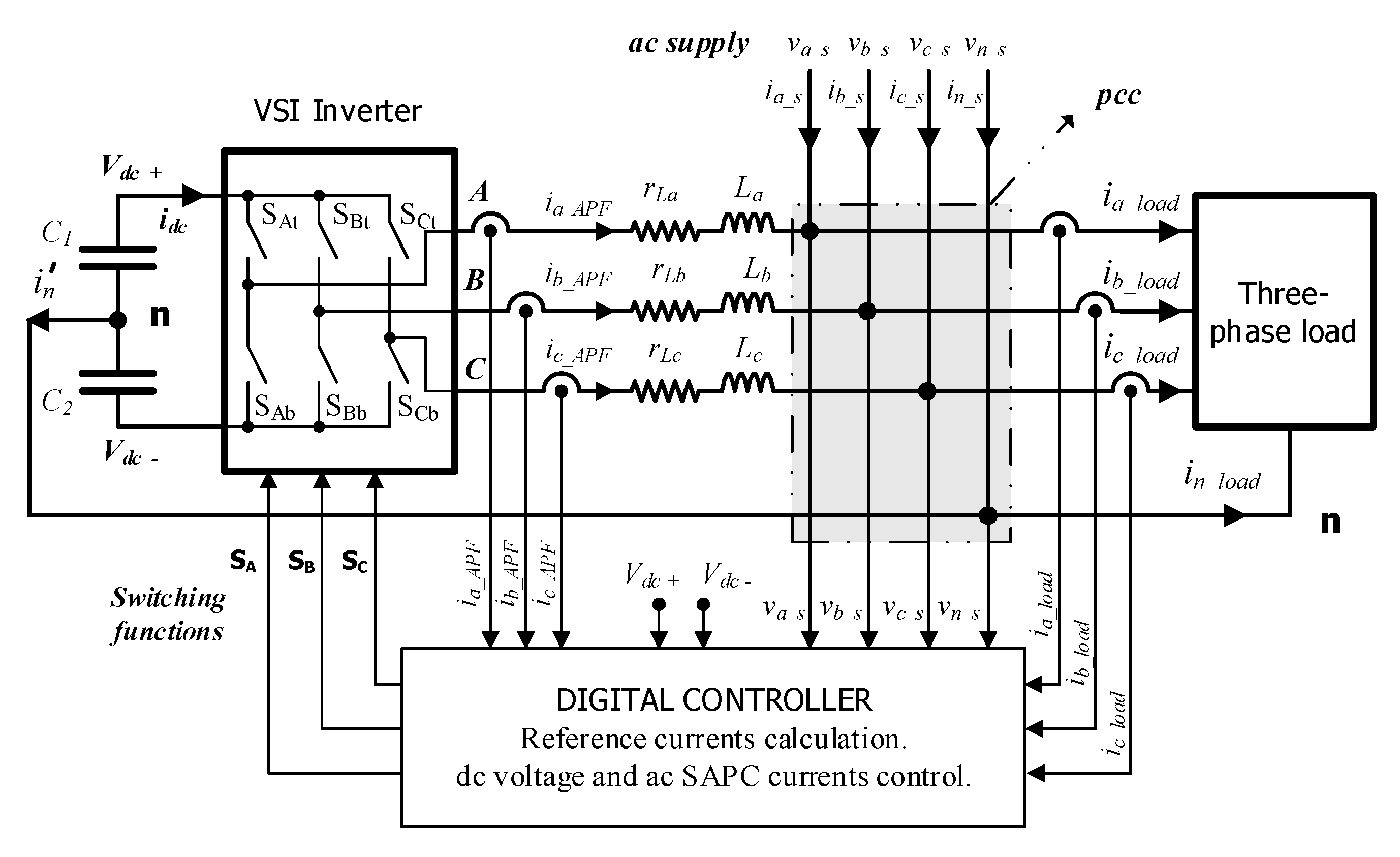
Consider the three-leg four-wire grid-tied power converter presented in
Figure 2. The converter operates as a three-phase voltage source inverter (VSI) connected to the ac power network through inductances
. Equivalent series resistance (ESR) of the dc bus capacitors and the resistive part of the inductances are neglected for clarity. The fourth wire connects the neutral wire of the power network to the dc bus midpoint. This power stage configuration is commonly used in SAPFs and can be treated as three independent single-phase converters sharing a unique dc bus. The VSI switches should be an IGBT–diode association allowing bi-directional current flow. The switches of a branch are controlled in a complementary fashion, meaning that at any time, only one switch per branch is in the ON state. Neglecting switching times, also for simplicity, only two states are possible and the per-phase equivalent circuit of
Figure 3 is obtained. The control system should include dc bus voltage regulation; dc bus midpoint voltage unbalances compensation and ac-side current control.
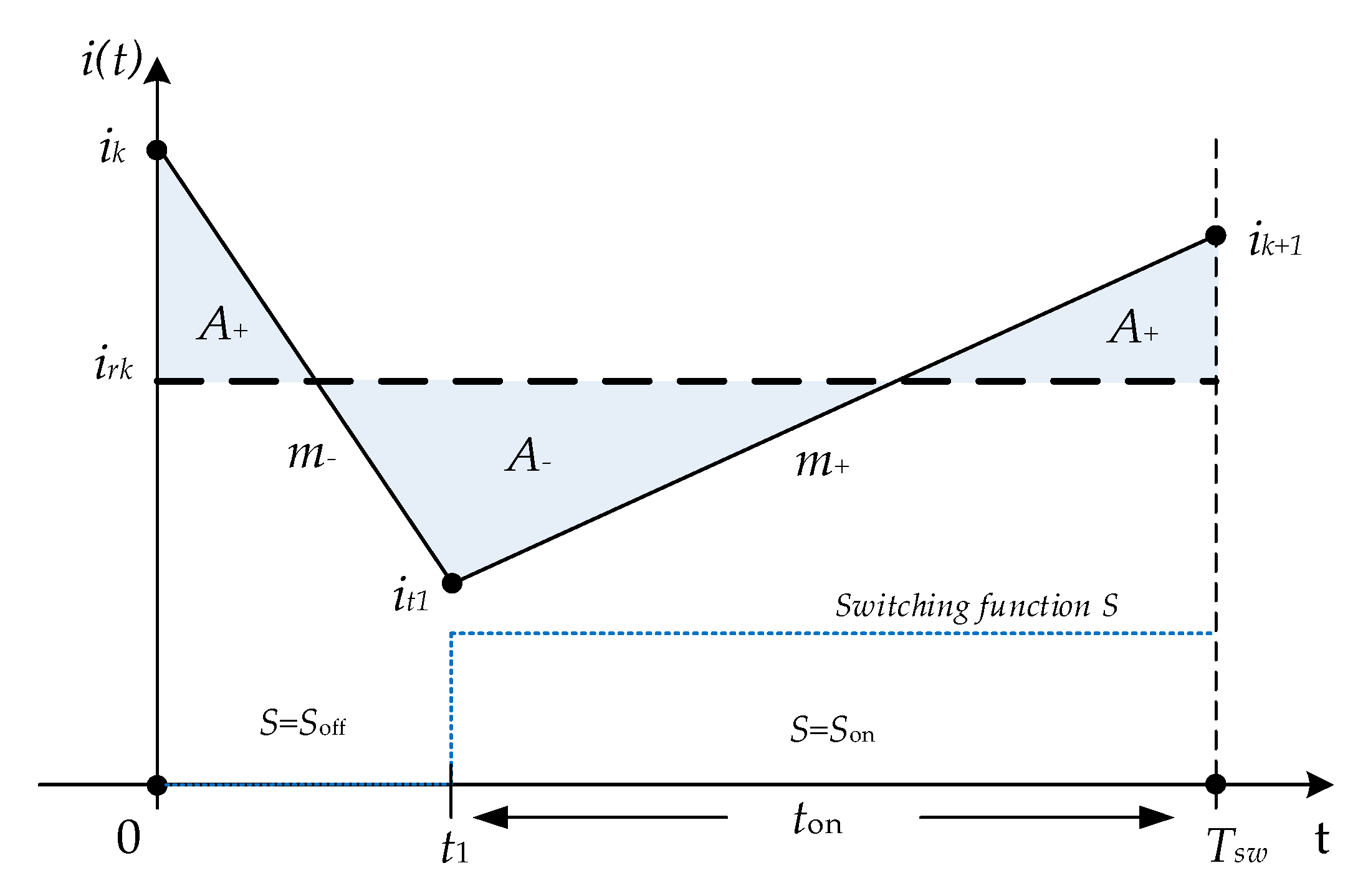
Consider now the application of one-cycle current control, with fixed switching period
, to the circuit of
Figure 3. The one-cycle control paradigm [
23,
24] is based on computing the control in one switching cycle, as shown in
Figure 4. As a result, given an initial current through the inductance
and a constant current reference value to be tracked
, the problem is to find the ON time (
ton or
t1 in
Figure 4) that allows the performance of optimal reference tracking. Subscript
, which refers to the converter phases, is hereafter omitted for clarity.
This work proposes a one-cycle control method that seeks to minimize the absolute value of the current error integral in a switching cycle, that is:
where
. Graphically, the above optimization problem is equivalent to the minimization of the sum of the gray areas in
Figure 4. The minimum value of the optimization problem is zero, which is achieved when positive areas
are equal to negative areas
. If the optimal value is greater than zero, then it provides the optimal ON time (
ton*) that minimizes the integral error.
The rationale behind this figure of merit lies in the fact that when the minimum value is achieved, and and are nearly constant for one switching cycle, the control provides, in one cycle, the same power as the one defined by the current reference. Note that, given the switching nature of the converter, it is impossible to track perfectly the reference in every instant within a switching cycle; however, the mean value of the signals over a switching cycle can be equal.
In the rest of the article, the following assumptions are considered:
The reference current is constant during the switching period.
For a switching cycle k, when S = Son, the phase current i(t) increases with slope , defined as , which is always positive because is always greater than On the other hand, when S = Soff, the phase current decreases with slope , defined as , which is always negative.
Slopes and are assumed constant during the switching cycle. For high switching frequencies (in the range of kHz), and are nearly constant for a switching period. Then, slopes and can be considered constant for the entire switching cycle. The error produced by this assumption is considered and proved not significant, so it does not justify the increased complexity.
3. One-Cycle Zero-Integral-Error
The optimal ON time
* is obtained by solving the following constrained optimization problem:
With the current error
defined as:
is the current at the switching point given by:
The optimization problem (2) can be solved analytically by first computing the one-cycle integral error as:
The integral of the error when the switch is ON is:
The integral of the error when the switch is OFF is:
Finally, adding both integrals yields the following expression:
As a result, the integral of the error is a quadratic polynomial in
, equivalently in
, defined as, and given by:
The polynomial has the following properties:
The quadratic function is convex, because .
The minimum of the function is always at , because and yields .
Note that the function to be minimized is not , but its absolute value . Its minimum ) can be obtained by the following procedure:
Compute . If , the optimizer is , and the optimal value is . This condition is equivalent to .
Compute . If , the optimizer is , and the optimal value is , because p(ton) is convex and, with a minimum at , if p(0) is negative, then p(0) is the maximum value for ton [0, Tsw] and as we take the absolute value , it follows that p(0) is positive and the minimum value for ton [0, Tsw]. This condition is equivalent to .
Finally, if , the optimal is obtained by the solution of , that is given by:
3.1. Control Algorithm
The control algorithm requires us to measure the phase current at the beginning of each switching cycle () in order to compute the current error . Depending on the value of the current error , the optimal control action to be applied is:
If , then .
If , then .
If , then
The following remarks are in order:
The optimization problem achieves the minimum value of 0 when . In this case, the control provides the one-cycle zero integral error.
In the case that or , the minimum value achieved is greater than zero and the one-cycle zero integral error property is no longer achieved, although the algorithm still minimizes its value. These cases arise when the value of the error is so large that it saturates the control action (i.e., or ).
In general, slopes and are not constant but time varying in each switching cycle. Hence, the slopes must be updated accordingly in each cycle.
3.2. Stability Analysis
Once
is obtained, a stability analysis is performed. The phase current at the end of switching cycle
is related to the current at the beginning
by:
Subtracting Equation (11) from the reference current in one-cycle
, the evolution of the error is obtained as:
The objective is to analyze the error evolution of Equation (12) when the optimal ON time (10) is applied. Substituting (10) into (12) and arranging terms, the following nonlinear iterated map is obtained:
First, the fixed points of the map are computed, that is,
. The fixed points are given by solving:
The next step is to determine the stability of the fixed point. For unidimensional iterated maps
, the fixed point
is stable if
. Particularizing the stability result to Equation (14):
Particularizing the derivative Equation (16) with the fixed point
given in (15):
Finally, the system is stable if:
Considering the equivalent circuit in
Figure 3, the stability condition (18) leads to an unstable behavior of the controller during the positive half-cycle of the supply voltages, where
is greater than
. Stability properties considering the switching pattern are analyzed and a stable controller for a complete voltage cycle is derived in
Section 4.
4. Stability and Switching Pattern
Consider the evolution of the phase current with the switching pattern shown in
Figure 5. In this case, the switching period starts in the OFF state and turns on at time
, remaining in the ON state until the end of the switching period.
Using this switching pattern, and following an analog procedure, i.e., the one in
Section 3, the one-cycle integral defines again a quadratic polynomial in
, given by
The polynomial has the following properties:
The quadratic function is concave, because .
The minimum of the function is always at , because and yields .
In an analogous manner to the previous section, the minimum of can be obtained by the following procedure:
Compute . If , the optimizer is , and the optimal value is . This condition is equivalent to .
Compute . If , the optimizer is , and the optimal value is . This condition is equivalent to .
Finally, if , the optimal ON time is obtained by solving , that is given by:
The stability analysis for the optimal
obtained with the new switching pattern is repeated. The resulting nonlinear map of the current error is, in this case:
The fixed point is given by:
As can be seen, the fixed point is equal in magnitude, but with opposite sign to the one previously computed in (15). Finally, the stability condition is shown to be:
That is complementary to stability condition (18) computed in
Section 3 with the switching pattern of
Figure 4. Summing up, the use of two distinct switching patterns (one for each half-cycle of the voltages) renders the one-cycle zero-integral-error current control stable.
Control Algorithm
This subsection summarizes the one-cycle zero-integral-error control algorithm. The control algorithm requires us to measure the phase current at the beginning of each cycle (
) in order to compute the current error
. Furthermore, the algorithm also requires computing the slopes
and
that, in general, are time varying at each switching cycle. The slopes are necessary to choose the stable switching pattern and to compute the optimal ON time. Hence, the slopes must be updated each cycle. The control algorithm is resumed in the flowchart of
Figure 6.
5. Simulation Results
Consider the power system presented in
Figure 7. A three-phase four-wire SAPF is used to achieve balanced currents, low current total harmonic distortion (THD) and unity power factor (PF) upstream from the pcc, where a linear load and a nonlinear load are connected.
The values used in the circuit
Figure 7 are:
La =
Lb =
Lc = 3 mH;
rLa =
rLb =
rLc = 0.1 Ω;
C1 =
C2 = 4.7 mF. The dc bus voltage is
Vdc = 450 V. Supply voltages (
va_s,
vb_s and
vc_s) are symmetrical with rms values equal to
Va_s = Vb_s = Vc_s = 120 V. Fundamental frequency is 50 Hz. SAPF switching frequency is 20 kHz. The nonlinear load uses a diode-based three-phase rectifier feeding a series R-L load. An unbalanced three-phase linear load is also connected at the pcc. Load values are presented in
Table 1.
Current slopes for each phase are given by: ; . where z = a, b, c and are the corresponding phase-shifts .
The power system has been simulated with Matlab/Simulink
®.
Figure 8 shows the load currents, while the active filter reference currents are presented in
Figure 9. By generating these currents, the SAPF achieves global compensation, meaning that reactive, unbalanced and distortion powers are reduced to near-zero values.
Figure 10 presents the current tracking performance of the controller proposed in
Section 4, while two details of this figure are presented in
Figure 11 and
Figure 12. The quality of the proposed control is demonstrated by the precise current tracking achieved. Note that a small current surge appears when a zero-crossing of the phase voltages occurs, exactly when the control changes the switching pattern. It appears because two consecutive high or low states are concatenated in the change of pattern. It also causes a small transient that stabilizes in several µs, as can be seen in
Figure 12. In order to reduce these surges, it is possible to modify the control algorithm to force the ON or OFF time to be small for the first switching period of the new pattern.
Figure 13 shows the current tracking error corresponding to the detail of
Figure 12.
Figure 14 shows the supply currents before and during the SAPF operation (
t > 0.055 s). The current waveforms become a set of balanced, sinusoidal currents, showing a THD of 1.83% and a PF equal to 0.9987. The error observed in the tracking of high reference derivatives can be reduced by increasing the switching frequency. However, for the one-cycle control technique, it means increasing control frequency and reducing computing time, as well as increasing the switching losses.
Finally,
Figure 15 presents the harmonic spectrum of supply currents obtained during compensation. Low-order harmonic components are small compared to the fundamental component, as indicated by the resulting THD value. Higher harmonics are concentrated around the switching frequency (order 400 for 20 kHz).
6. Experimental Results
Figure 16 shows the prototype implemented in the lab to perform the experimental tests. SAPF has been implemented by means of a Toshiba PM75CG1B120 (75 A, 1200 V) three-phase power stage switching at 20 kHz. The scheme of the power system matches the one shown in
Figure 7. SAPF component values (dc bus capacitors and phase inductances) as well as the load components are the same as those presented for the simulation example in
Section 5. A Pacific Power A-360MX three-phase power supply generates the 120 V rms three-phase supply voltages. A dc bus voltage controller assures
and a capacitor voltage-balancing controller keeps the voltage equally distributed between the capacitors [
2]. A LeCroy waveJet 324 oscilloscope (200 MHz-2 GS/s) is used to carry all measurements and to obtain the voltage and current figures presented in this section.
The proposed one-cycle control requires high-speed computing, because it has to calculate the reference currents and the ON times of the next switching period in a few microseconds. To obtain good current tracking, it also needs accurate measurements of load and SAPF phase currents at the beginning of the switching period, as shown in
Figure 4 and
Figure 5. Dc bus and supply voltage measurements are not so time-critical because they change slowly compared with the switching period. However, to wait until the end of the cycle means overlapping part of the next switching period with the calculations needed to compute its corresponding ON time. This is a problem because no action is possible until the computations are finished.
To avoid this problem, SAPF currents and load currents are measured using six AMC1303E2520 sigma-delta modulators that feature 20 mega samples per second (MSPS), an internal clock and Manchester modulation. Using these sigma-delta modulators, 40 high-precision samples per switching cycle (at 800 kSPS) are obtained, allowing us to precompute the slope of each one of the six currents and their values at the end of the switching period, whilst avoiding possible mismeasurements due to semiconductor switching. This forward calculation allows for computing the next ON time, avoiding the need to wait until the end of the switching period to sample the currents and compute the ON times. It is also important to remark that, due to the switching times of the semiconductors in the power stage, a dead-band is needed. Considering this restriction, minimum and maximum values for ton could be limited to 5% and 95% of the switching period, respectively. This characteristic also conditions the dc voltage level needed to track reference currents, which must be slightly higher, consequently increasing the current ripple of phase currents.
In order to carry out these high-speed tasks, a Texas Instruments dual core TMS320F28379D microcontroller has been selected. This digital controller features up to 800 MIPS (200 MHz), and includes two programmable control law accelerators (CLAs), an IEEE 754 floating-point unit (FPU), a trigonometric math unit (TMU), eight sigma-delta filter module (SDFM) input channels and many other peripherals. Combining the powerful microcontroller and the sigma-delta modulators, the proposed control has been implemented and the experimental results are shown in the next figures.
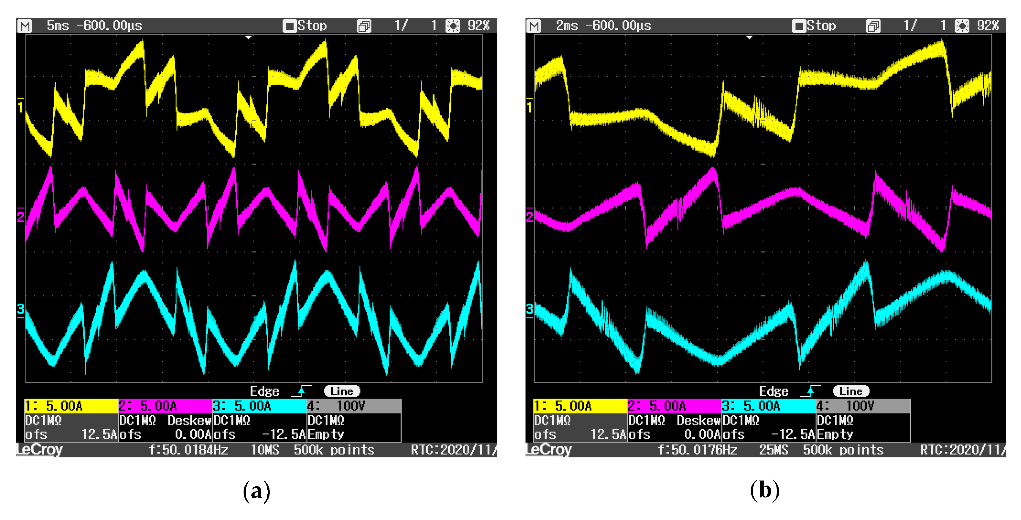
Figure 17a shows the supply voltages, a set of three-phase balanced voltages of 120 V rms. The load currents are shown in
Figure 17b and correspond to the mixed load presented in
Table 1. The currents delivered by the SAPF to achieve global compensation are presented in
Figure 18a and details of SAPF phase currents are presented in
Figure 18b and
Figure 19. These detailed waveforms show the good shape of the currents, in both positive and negative half-cycles. As expected, a small surge and a short instability appear at zero-crossings of the supply voltages, when the control changes the switching pattern. The excellent performance of the current tracking is validated by the good supply current waveforms obtained during the compensation.
Figure 20 shows how supply currents become a set of balanced sinusoidal currents. The small surges in the waveforms have two causes. As mentioned before, there are surges caused by the change of switching pattern at zero-crossings of voltages, and second, there are surges due to the normal error produced in tracking the sudden slope changes in the reference currents. The supply current THD is 2.8% and PF reaches a value of 0.997. A slight increment in the current THD value compared with the one obtained in the simulation can be appreciated. This is caused by the real characteristics of the semiconductors and tolerances of the passive components used in the experimental setup.

 ,
, 


