1. Introduction
Now mobile electronic devices such as laptop and tablet computers, smart phones, and smart watches require displays with high resolution and low power consumption [
1,
2]. As a result, a new thin-film transistor (TFT) backplane technology has been employed in mobile display products, so called low-temperature polycrystalline silicon and oxide (LTPO) TFT technology. It uses LTPO TFTs to improve the circuit performance by taking advantage of the high mobility and high reliability of low-temperature polycrystalline silicon (LTPS) TFTs as well as the extremely low off-state current of oxide TFTs.
LTPO TFT circuits have been studied for many years. LTPO TFTs were mainly used in complementary metal oxide semiconductor (CMOS) inverter circuits [
3,
4]. They were called hybrid CMOS circuits to distinguish them from the conventional CMOS circuits using polycrystalline silicon TFTs. They used a p-type LTPS TFT and an n-type oxide TFT to implement the pull-up and pull-down transistors of the inverter circuit, respectively. They adopted the coplanar LTPS TFT structure and etch-stopper layer to protect the active region of oxide TFT. After that, a CMOS inverter [
5], a level shifter [
6], and an operational amplifier [
7] with a simpler LTPO TFT process were developed using the coplanar LTPS TFT without etch-stopper layer. They adopted multiple inverter circuits comprising the LTPO TFTs to generate output signals. Additionally, an LTPO TFT structure comprising both coplanar LTPS and oxide TFT was developed recently [
8].
Recently, display circuits comprising LTPO TFTs have been developed actively. Apple Inc. presented a pixel circuit for active-matrix organic light emitting diode (AMOLED) displays using an LTPO TFT process [
9]. The LTPS and the oxide TFTs had top-gate and bottom-gate structures, respectively. The LTPS TFTs were used in the integrated gate driver and the pixel circuits. The oxide TFT was placed in the pixel circuit as a switching device to maintain the voltages of image data for a long time. The display panels using LTPO TFTs were first commercialized in the smart watch. Japan Display Inc. developed a different LTPO TFT structure and applied it to display circuits of liquid crystal displays (LCDs) [
10,
11]. The oxide and LTPS TFTs had a top-gate structure. A light shield layer was placed under the oxide TFT to prevent the active layer from light instability of oxide TFTs. The oxide TFTs were fabricated after the LTPS TFT process and used in each pixel to achieve low frame frequency. The LTPS TFTs were used in gate drivers and demultiplexers for the peripheral display circuits.
To reduce the power consumption of displays, memory-in-pixel (MIP) circuits have been developed. The research on MIP circuits first originated from the development of the integration of display circuits on a glass substrate [
12]. The LTPS TFTs feature high mobility and strong reliability, which enable the design of complicated display circuits such as timing controllers, common drivers, gamma circuits, digital-to-analog converters (DACs), and power-supply circuits onto the glass. The objective of the MIP circuit was to integrate the memory devices into the pixel area. Based on this motivation, many studies to reduce the power consumption of display panels were undertaken for several years [
13,
14,
15,
16,
17,
18]. The power consumption of displays employing the MIP circuits can be reduced by virtue of low-frame-frequency driving. H. Kimura et al. [
13] developed a reflective LCD with an MIP circuit. They added a digital memory circuit to the conventional LCD pixel structure based on LTPS TFT backplane. M. Senda et al. [
14] introduced a 1-bit SRAM circuit into each pixel to realize the MIP circuit. L.-W. Chu et al. [
15] proposed an analog MIP circuit using LTPS TFTs. M. Tamaki et al. [
16] developed an MIP circuit which embeds SRAM circuits in each pixel for reflective-type LCD based on LTPS TFTs. The reflective-type LCDs with their proposed MIP circuit has been commercialized for various display applications such as digital signage, smart watches, and electronic shelf labels. Utilizing the memory property of a ferroelectric gate insulator, a low-power LCD was proposed using oxide and ferroelectric memory TFTs (Fe-MTFTs) [
17]. The Fe-MTFTs exhibited memory characteristics because of their ferroelectric gate insulator. The Fe-MTFTs were used as a driving transistor. However, the ferroelectric gate insulator had reliability problems. An MIP circuit was proposed where the driving transistors were composed of oxide TFTs [
18]. The oxide TFTs still suffered from stability problems, and were more vulnerable than LTPS TFTs [
19,
20,
21,
22,
23].
In this paper, a new MIP circuit using LTPO TFTs is proposed. We expect that the power consumption will be decreased due to greatly reduced frame frequency. Furthermore, LTPS TFTs enable high stability and flicker-free LCDs by directly driving pixels. In
Section 2, we review a simple memory cell including LTPO TFTs. In
Section 3, we propose the MIP circuit based on the memory cell presented in
Section 2. In
Section 4, the performance of the proposed circuit is demonstrated.
2. Review of Memory Cell Comprising LTPO TFTs
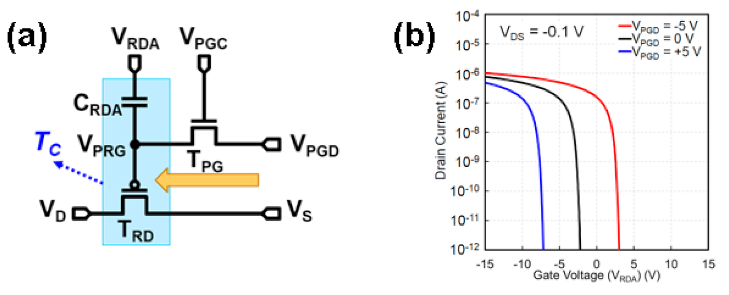
This section reviews the memory cell comprising LTPO TFTs proposed in [
24]. The memory cell consists of two transistors and one capacitor, as shown in
Figure 1a. T
PG is a programming transistor to transfer programmed voltage (V
PGD) signal to the gate node of T
RD, V
PRG. T
RD is a reading transistor. Here, a p-type LTPS TFT is used for T
RD and an n-type oxide TFT is used for T
PG. C
RDA is a storage capacitor used to maintain the charges stored in V
PRG node. The serially connected T
RD and C
RDA act as a memory cell transistor, T
C. The circuit has five control signals: V
PGC, V
PGD, V
RDA, V
D, and V
S. V
PGC is used to turn on or off T
PG. V
PGD is a programming voltage of the memory cell. V
RDA is a read-address voltage used to read out data stored in the memory cell. V
D and V
S are drain and source voltages of the memory cell, respectively, which can be used for bit-line voltages of the memory cell.
Figure 1b shows simulated transfer characteristics of T
C depending on the programmed level of V
PGD [
24]. After programming V
PGD through T
PG, the voltage level of V
RDA was swept and V
DS of −0.1 V was applied. As a result, the threshold voltage of T
C can be easily modified by changing V
PGD. When V
PGD had a positive value such as 5 V (a blue line), the electrons were attracted to near the channel of T
RD and thus the transfer characteristic of T
C was negatively shifted. On the contrary, when a negative V
PGD such as −5 V (a red line) was applied, the electrons were repelled from the channel of T
RD. Thus, the transfer characteristic of T
C was shifted to the positive direction. Consequently, the polarity of V
PGD determines the shift direction of transfer characteristics of T
C. In the next section, we propose a pixel structure based on the memory cells.
3. Proposed Pixel Circuit
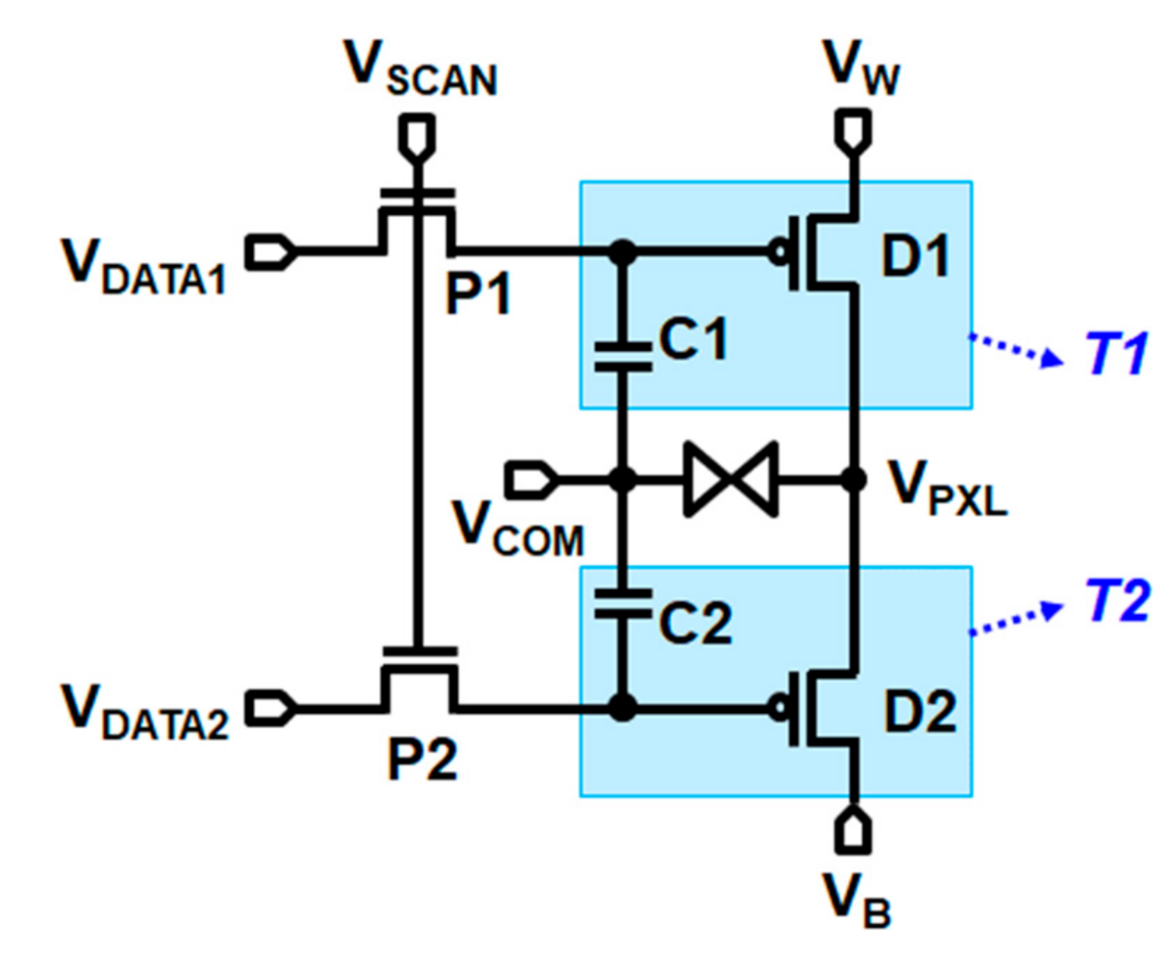
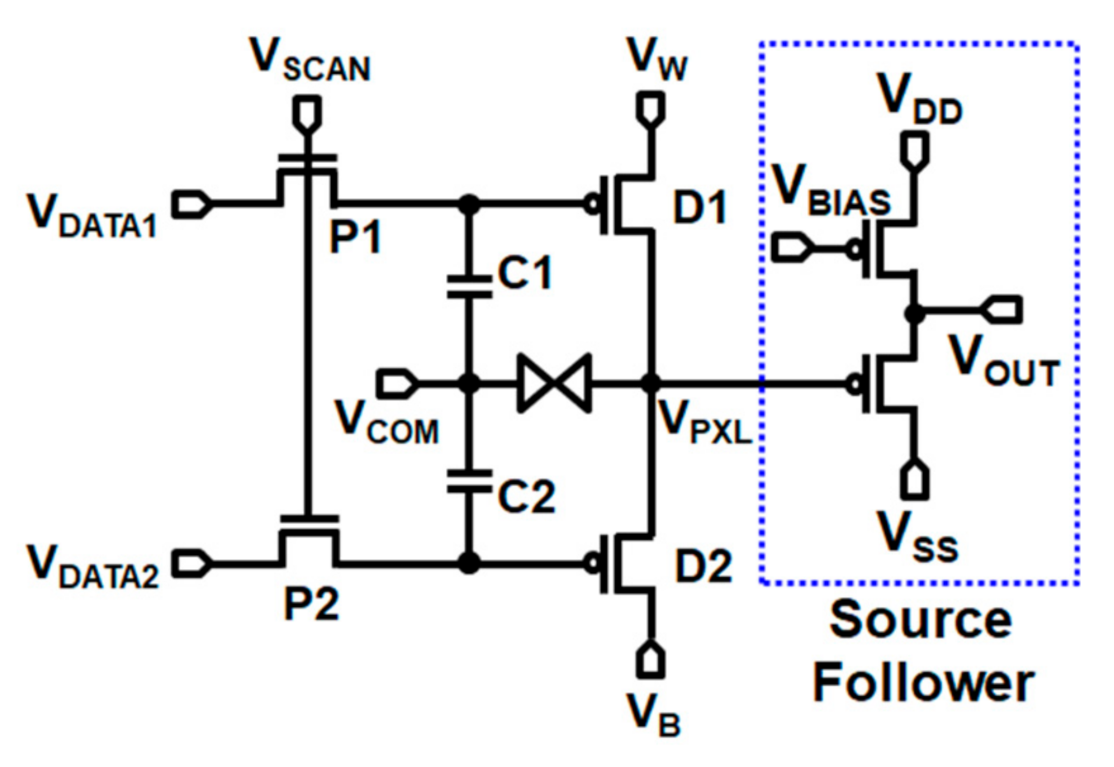
Our proposed MIP circuit comprising LTPO TFTs is shown in
Figure 2. Four transistors and two capacitors are used in a unit pixel circuit. D1 and D2 are driving transistors fabricated with p-type LTPS TFTs. They drive the pixel with V
W and V
B, respectively. P1 and P2 are programming transistors composed of n-type oxide TFTs. They apply V
DATA1 and V
DATA2 to the gate terminals of D1 and D2, respectively. C1 and C2 are storage capacitors to keep programmed voltages.
The proposed circuit contains five control signals: VSCAN, VDATA1, VDATA2, VW, and VB. VSCAN turns on the programming transistors. Both VDATA1 and VDATA2 determine the on/off-state of the driving transistors. VW and VB are signals to display white and black images, respectively. They have positive (VW+ and VB+) and negative levels (VW− and VB−) for polarity inversion of liquid crystal (LC) cells. The serially connected D1 and C1 are defined as T1 and the serially connected D2 and C2 are defined as T2. T1 and T2 act like memory cell transistors. Thus, VTH,T1 and VTH,T2, the threshold voltages of T1 and T2, can be shifted according to VDATA1 and VDATA2, respectively.
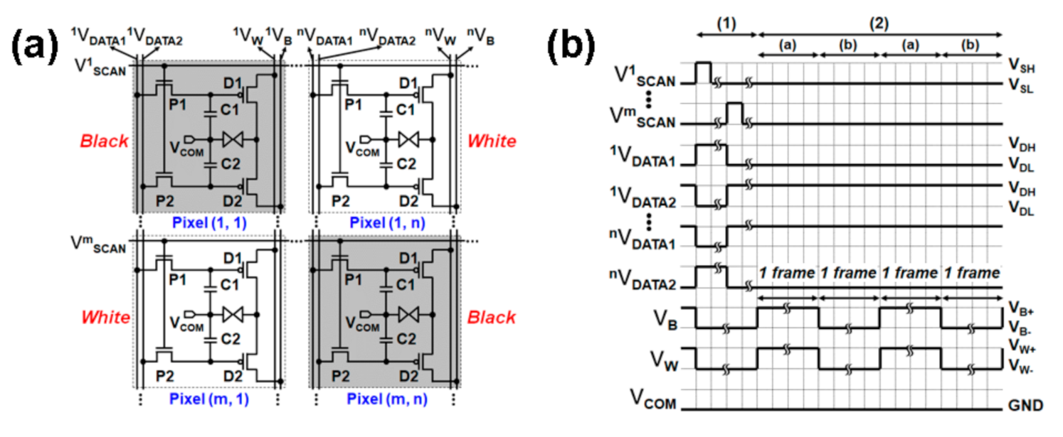
Figure 3a shows a circuit diagram to describe multiple pixel operations. The pixels of the m-th row are connected to V
mSCAN.
nV
DATA1,
nV
DATA2,
nV
W, and
nV
B are connected to the pixels in the n-th column. V
COM is the ground level throughout the circuit operation, as shown in
Figure 3b. The operation of the circuit is divided into two steps: programming and displaying.
(1) Programming: During the period (1), VSH turns on P1 and P2. When we display black in the pixel (1, 1), 1VDATA1 with VDH and 1VDATA2 with VDL are transferred to the gate terminals of D1 and D2 in the pixel (1, 1), respectively, when V1SCAN is VSH. Likewise, to display black in the pixel (m, n), nVDATA1 with VDH and nVDATA2 with VDL are programmed in the pixel (m, n), respectively. Here, VDH has a positive value, whereas VDL is a negative one. Thus, VTH,T1 shifts to the negative direction, whereas VTH,T2 is positively shifted. As a result, D1 turns off and D2 turns on since they are p-type TFTs. The pixel voltages in the pixel (1, 1) and pixel (m, n) are charged to VB+ for black image.
(2) Displaying: During the period (2a), VSL turns off P1 and P2. The gate-to-source bias (VGS) of D1 and D2 remain constant until the next program time. Because the driving transistors, D2s in the pixel (1, 1) and pixel (m, n), directly drive the pixel with VB, there is no kickback while displaying image, so that there is no flicker problem. During the period (2b), VW and VB become negative polarities (VW− and VB−), for the polarity inversion. Then, the period from (2a) to (2b) is repeated so that the polarity inversion can be continued without additional programming.
When we display white in the pixels (m, 1) and (1, n), 1VDATA1/nVDATA1 with VDL and 1VDATA2/nVDATA2 with VDH are transferred to the gate terminals of D1 and D2, respectively, in the pixels (m, 1) and (1, n). As a result, during the period (2a), the pixels (m, 1) and (1, n) are charged to a positive level (VW+) and then changed to a negative one (VW−) during the period (2b).
4. Results
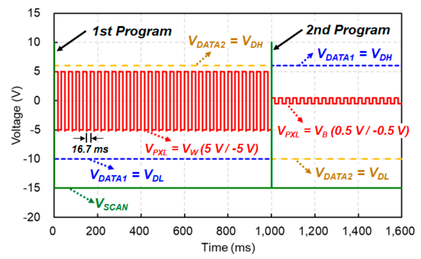
The circuit operation was verified with spice simulation, whose parameters were extracted from the fabricated LTPO TFTs.
Figure 4 shows simulated results to verify the programming operation. The voltage levels of V
DH, V
DL, V
SH, and V
SL were 6 V, −10 V, 10 V, and −15 V, respectively. It was assumed that an LCD worked as a normally black mode. V
B+, V
B−, V
W+, V
W−, and V
COM were 0.5 V, −0.5 V, 5 V, −5 V, and 0 V, respectively. The turn-on time of V
SCAN was set to 10 μs.
As shown in
Figure 4, we set V
DATA1 and V
DATA2 to V
DL and V
DH, respectively, to display white at the 1st program. Thus, V
TH,T1 was positively shifted and V
TH,T2 was negatively shifted, so that D1 turned on and D2 turned off. We observed that the pixel voltage, V
PXL, became 5 V (V
W+) after the 1st program, which means that D1 turned on successfully. After 16.7 ms, the polarity inversion was successfully achieved as shown in
Figure 4. At the 2nd program, V
DATA1 and V
DATA2 were set to V
DH and V
DL, respectively. Thus, it is confirmed that the pixel voltage was charged to V
B+ of 0.5 V and polarity inversion was performed again.
We investigated the long-term operation of the proposed circuit as shown in
Figure 5. There was a study about measuring off-state current of oxide TFTs. K. Kato et al. [
25] reported that an oxide TFT has an off-state current of approximately 10
−21 A/μm. During the simulation, we set the off-state current of the oxide TFT to 10
−15 A because it was small enough to verify our circuit operation. As shown in
Figure 5a, even if V
DATA1 and V
DATA2 were changed to 0 V after one second, the gate voltages of D1 (V
G,D1) and D2 (V
G,D2) were maintained constantly for a long time. V
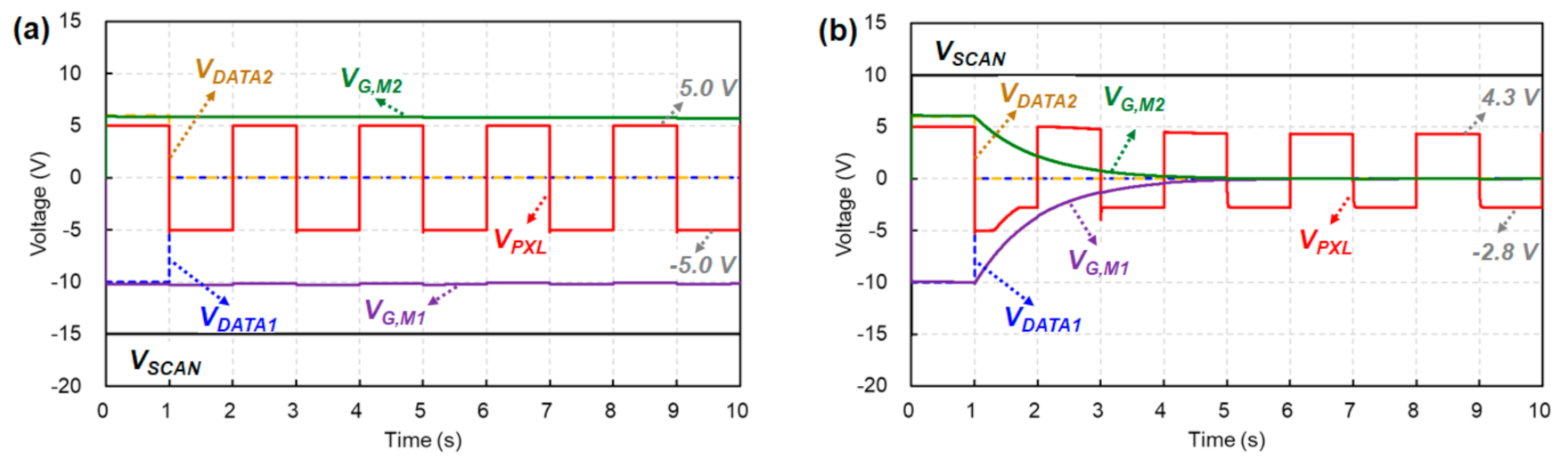
PXL also successfully reached its target level ranging from 5 V to −5 V. We observed that the programming transistors retained the programmed voltages for longer than ten seconds. This is attributable to the remarkably low off-state current of the oxide TFTs. Consequently, the simulated results verify that the proposed pixel circuit can operate at a far lower frame frequency (or programming frequency) than conventional displays.
Figure 5b shows simulated results for comparison when the programming transistors are p-type LTPS TFTs. We set the off-state current of LTPS TFTs to approximately 10
−11 A for this simulation. The LTPS TFTs feature higher stability [
19,
20,
21] and larger off-state current than oxide TFTs. Thus, V
G,D1 and V
G,D2 could not maintain their voltages constantly for hundreds of milliseconds after V
DATA1 and V
DATA2 became 0 V as shown in
Figure 5b. Since D1 and D2 turned on simultaneously, we observed that V
PXL was distorted in the range from −2.8 V to 4.3 V.
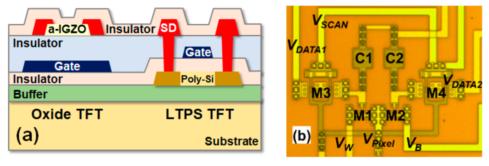
The proposed pixel circuit was fabricated by using the LTPO TFT process.
Figure 6 shows a cross section of the LTPO TFTs and an optical image of the proposed circuit. The LTPS and oxide TFTs used a top-gate and bottom-gate structure, respectively. They shared the same layer of gate metal. Thus, process steps were reduced by these structures.
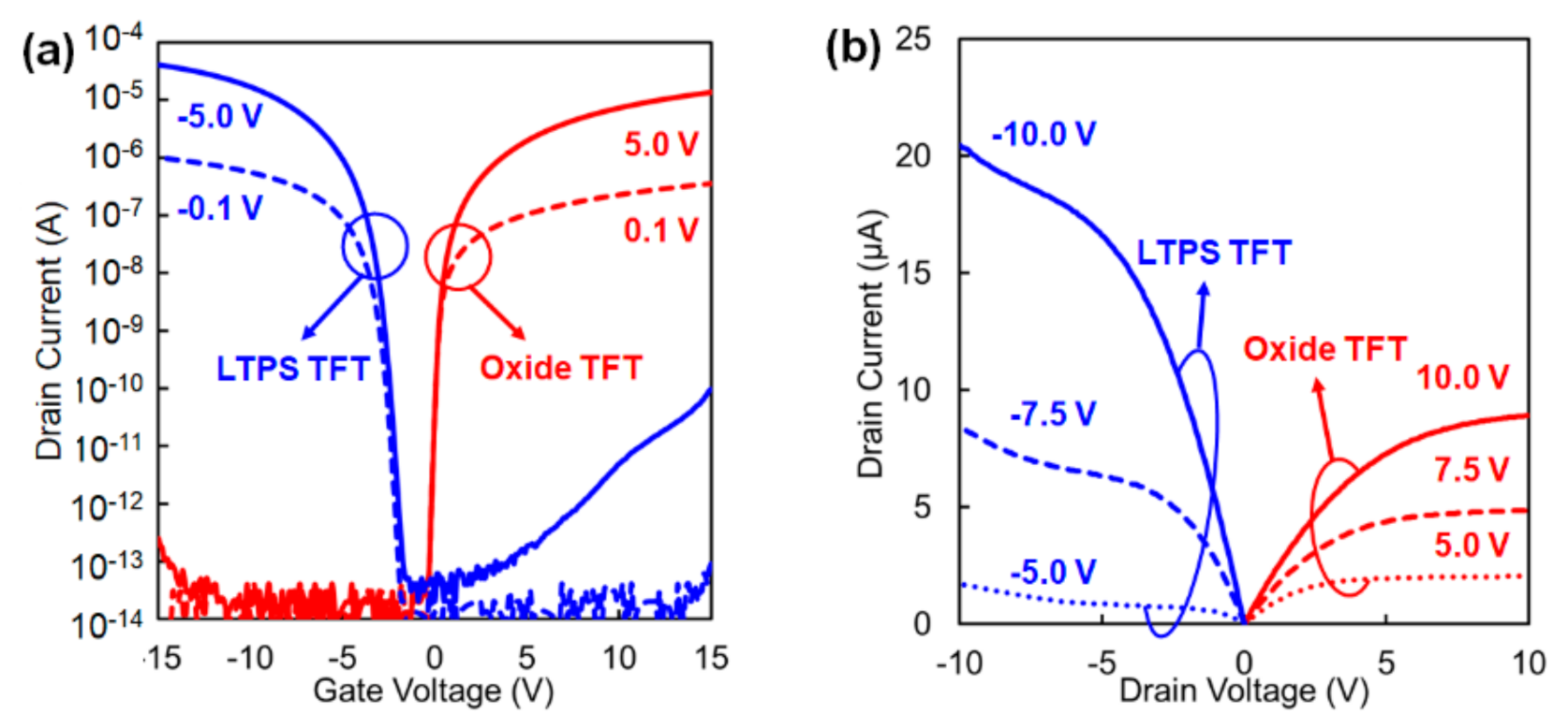
Figure 7 shows the characteristics of fabricated n-type oxide (red lines) and p-type LTPS (blue lines) TFTs. The width and length of both TFTs were 4 μm and 5 μm, respectively. The threshold voltages (V
TH) of oxide and LTPS TFT were −0.1 V and −2.3 V, respectively. The off-state current of the LTPS TFT showed much higher than that of the oxide TFT when a drain bias was −5 V.
We also verified the circuit operation with measurement results. Measuring the pixel voltage directly with an oscilloscope probe can result in distortion of measured signals since the probe impedance is not infinite. To solve this problem, a source follower circuit was used as shown in
Figure 8. V
DD, V
SS, and V
BIAS were 10 V, −6 V, and 6 V, respectively. The change in V
PXL can be investigated without distortion by measuring V
OUT.
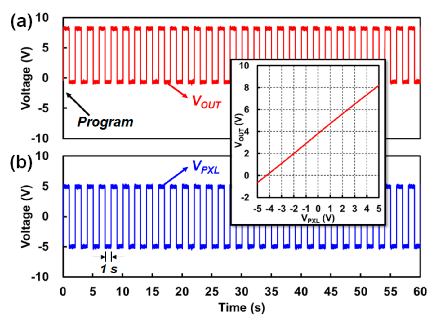
As shown in
Figure 9a, we measured V
OUT while the circuit operated for 60 s. Then, we converted V
OUT into V
PXL as shown in
Figure 9b by using a voltage transfer characteristic (inset). V
DATA1 and V
DATA2 were programmed only once. We set V
DATA1 and V
DATA2 to −5 V (V
DL) and 5 V (V
DH), respectively. As a result, V
OUT became 8.2 V, which corresponds to V
PXL of 5 V (V
W+) after programming. Then, the polarity inversion operated at every second of time. V
OUT became −0.6 V, corresponding to V
PXL of −5 V (V
W−). Therefore, the successful operation of the proposed MIP circuit for 60 s was proved without any problem after programming only once as shown in
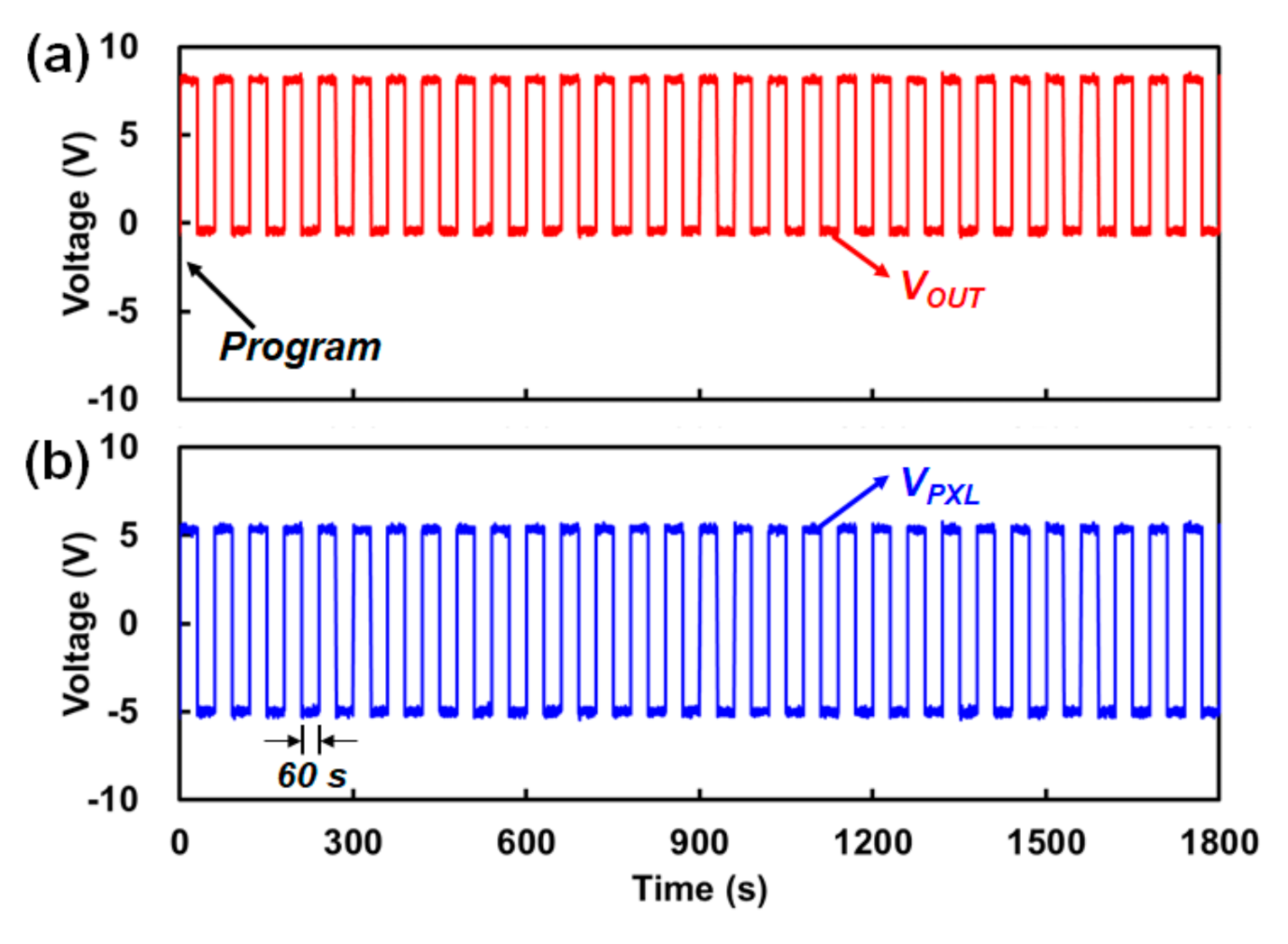
Figure 9. Furthermore, we evaluated how long the circuit can operate without additional programming. We inverted the pixel polarity at every one minute to make sure the polarity inversion worked well. As a result, we verified that the circuit operated for even 30 min without further programming as shown in
Figure 10.
5. Discussion
The power consumption of the LCD comprising the proposed MIP circuit was compared with that of a conventional LCD. It was assumed that the conventional LCD has a pixel structure with one transistor and one capacitor. The resolutions of both LCDs were set to 1920 × 1080 (full high definition). Thus, when we display a horizontal line pattern driven by the column inversion and a full white pattern driven by the dot inversion, both LCDs consume the highest power. Thus, the dynamic power consumption of these two cases were calculated as in [
26]. The dynamic power of the conventional LCD (
PDyn,C) for a full white pattern based on the dot inversion is expressed as
CCL, ΔV
W, and
fV are the capacitance of a column line, the voltage magnitude of the white signal, and a frame frequency, respectively. To calculate the power consumption of the proposed LCD, we should consider the dynamic power (
PCL) of the column lines and the dynamic power (
PPL) of pixel driving lines, V
W and V
B. The power consumption of the proposed MIP circuit for a full white pattern based on the dot inversion is expressed as
CPL and
CPXL are the capacitance of a pixel driving line (V
W or V
B) and a pixel, respectively. ΔV
DATA and ΔV
B are the voltage magnitude of the data and black signal, respectively.
fI is a polarity inversion frequency. When the proposed LCD displays a full white pattern driven by the dot inversion, ΔV
DATA is 0 V, so that
PCL is 0 W. The dynamic power consumption of the proposed LCD (
PDyn,P) is the sum of
PCL and
PPL, which is expressed as
CCL and CPL were set to 100 pF, and CPXL was 1 pF.
Dynamic power consumption (
PSCAN) at scan lines applied by V
SCAN is calculated as follows:
where
CSCAN is the load capacitance of a scan line.
CSCAN and V
SCAN are 180 pF and 25 V, respectively.
PSCAN is about 2 μW. As a result, the dynamic power consumption at scan lines is negligible. Thus, we do not include
PSCAN in the dynamic power consumption.
Table 1 shows calculated results of the power consumption. The proposed LCD consumes much less power than the conventional one. Compared with conventional LCD, the power consumption of the proposed LCD becomes 0.02% when operating in dot inversion or 0.32% when operating in column inversion. The dynamic power consumption is significantly increased if signal lines are charged and discharged at a high frequency. However, the characteristics of oxide TFTs used as the programming transistors can greatly reduce the frame frequency down to 1/60 Hz, as shown in
Figure 9. We set the frequency of the polarity inversion,
fI, to 0.5 Hz in the measurement. However, the frequency can be further decreased unless an image sticking effect from LCs occurs [
27], by virtue of direct driving of each pixel in the proposed circuit. Thus, the proposed LCD can considerably reduce the power consumption because of such a low operation frequency. In addition, the LTPS TFTs as driving transistors directly drive each pixel continuously, which can provide high stability and flicker-free LCDs. Therefore, the LCD comprising the proposed MIP circuit is expected to be very suitable for displays, which show still images for a long time such as digital signage.
The usefulness of the proposed circuit is not limited to just pixel circuits. LTPS TFTs enable high-resolution displays as well as various types of display circuits such as integrated gate drivers and demultiplexers due to high mobility and stability. Therefore, the proposed circuit with LTPO TFTs is very applicable to a whole display panel.


