1. Introduction
Single Event Effect (SEEs) are undesired erroneous effects in digital integrated circuits caused by ionizing radiation. With CMOS device scaling, SEEs have become an increasingly important reliability concern leading to severe soft-error rates in advanced systems [
1]. Not only in nuclear instrumentation or space applications, even in critical commercial applications such as autonomous transport systems soft errors have become an increasingly important concern. With the growing complexity of digital circuits and clock frequencies, the overhead of redundancy should be reduced to a minimum. This paper addresses both Single Event Transients (SETs) and Single Event Upsets (SEUs). SETs are temporal erroneous signals which originate from the charges generated by the incident particles which are collected by the transistor in a combinational cell. They will recover over time, as can be seen on
Figure 1 [
2]. However if the SET propagates to a sequential cell like a flip-flop and occurs within the setup and hold times of the registers near a clock edge, the SET is latched leading to an incorrect logical state which is also known as an SEU as is shown in
Figure 1. The probability of such latching increases proportionally with higher clock frequencies [
3,
4]. SEUs can also occur when charged particles directly hit sequential digital circuits such as latches and flip-flops. When the register involves a bit-flip, this erroneous signal may remain in the digital system and can even propagate to other digital modules resulting in a failure. For example, an SEU could change the state of an Finite State Machine (FSM) temporarily impacting the entire system. SEUs can thus originate from direct upsets in the registers or as a result from SETs in the combinational logic, latched during clocking.
Triple Modular Redundancy (TMR) can be used to protect digital logic from SEEs. It uses redundant logic with majority voters to correct logic signals [
5]. TMR only works if only single errors occur in the digital logic, hence Multi Bit Upsets (MBUs) in common logic signals can be catastrophic for TMR. Nowadays complementary metal oxide semiconductor (CMOS) technologies have scaled to the point that MBUs have become a serious concern since a single particle can affect multiple gates simultaneously [
6,
7,
8]. This was less important in old CMOS technologies where single particles only affected single digital cells. However, with proper placement techniques, the fault tolerance can be ensured without compromising speed or power consumption in the design which is addressed in this paper.
Historically, several methods were developed to address trade-offs in TMR designs like power consumption and area efficiency. Full TMR is the most robust and most complete form of redundancy. In this approach, both the flip-flops, clock-tree and combinational logic cells are triplicated [
9,
10]. However, the drawbacks of this approach are the high number of resources (digital gates) and power consumption. Nevertheless it is the most solid and secure form of TMR. One of the competing methods is temporal time redundancy [
11]. In this method, only flip-flops are triplicated which are clocked with 3 skewed clocks. The combinational logic is not redundant. The skew between the clocks must be larger than any possible SET, hence only one flip-flop could possibly latch an SET. This method has proven its usage in many applications [
12]. However its major drawback is its limited clock frequency since clock skew places strict timing constraints on the design typically resulting in sub-GHz timing performance. Henceforth, many high-speed mixed-signal digital modules are based the original TMR approach. Additionally, Error Detection and Correction (EDAC) codes can also be used for radiation hardness assurance. They are usually placed surrounding the sequential cells to correct for any SEUs. Depending on the coding scheme, EDACs are also vulnerable to MBUs which must be mitigated as well and might be more difficult to ensure compared to TMR. The coding and decoding logic also adds to additional timing overhead which might significantly slow down the critical datapaths.
As indicated above, TMR only works if single errors occur. In deep-submicron technologies, proper physical implementation is required to ensure no MBUs occur between cells of the same TMR logic branch. This paper presents an innovative optimised physical placement methodology for full TMR design.
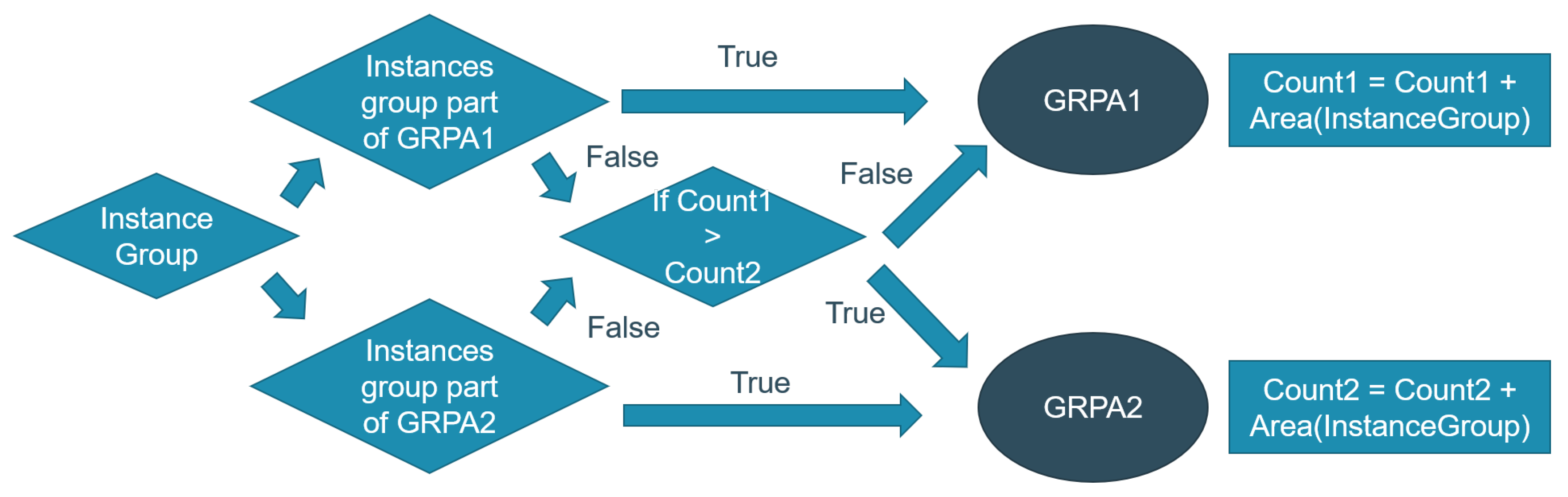
2. 3 Block Approach
One the most frequently used methods for physical implementation of TMR designs is by separating A-B-C logic in 3 different areas. Hence, a floor plan is created with 3 blocks (named A, B and C) as is shown on
Figure 2. All flipflops are constrained to their specified block A-C, the combinational logic and the clock tree will intrinsically follow the placement of the flipflops. However, each sequential net has 6 cross domain (A-C) interconnections(voter inputs) leading to long nets that transverse across the entire floorplan. Hence, the power consumption increases, and the net connections between the flipflops become congested.
As the design size increases, the length and the routing will be more complex resulting in increased routing congestion and power consumption due to additional buffers inserted by the place-and-route tools in the cross domain voted nets to meet timing constraints. Hence, power consumption and routing complexity is the main concern limiting its usability small or low frequency designs.
4. Simulated Analysis
Different comparative studies were performed with either the interleaved, the improved interleaved method or the standard 3 block approach to evaluate the efficiency and performance of this new placement and floorplanning technique. As benchmark, a design with eight identical and independent high-speed counters was used. To introduce more complicated standardised data paths, the counter dimensions (widths) and count of the benchmark models were varied. Larger counter widths would indicate a more complex datpath. More counters resemble a larger overall design in order to evaluate if the techniques scale with increasing design widths. The designs have been implemented and analyzed using the Cadence Innovus Computer Aided Design (CAD) tools. To guarantee a timing critical design, the timing limitations were selected to be near the technology boundaries. In the analysis, power consumption, net length, net capacitance and routing density were evaluated for each method. The slice height and spacing of the interleaved techniques was chosen as 7.2 m, whereas the 3 block technique has 7.2 m block spacing. This number aligned with the cells’ row heights. Finally, the timing, power and region reports from pace-and-route tools were extracted.
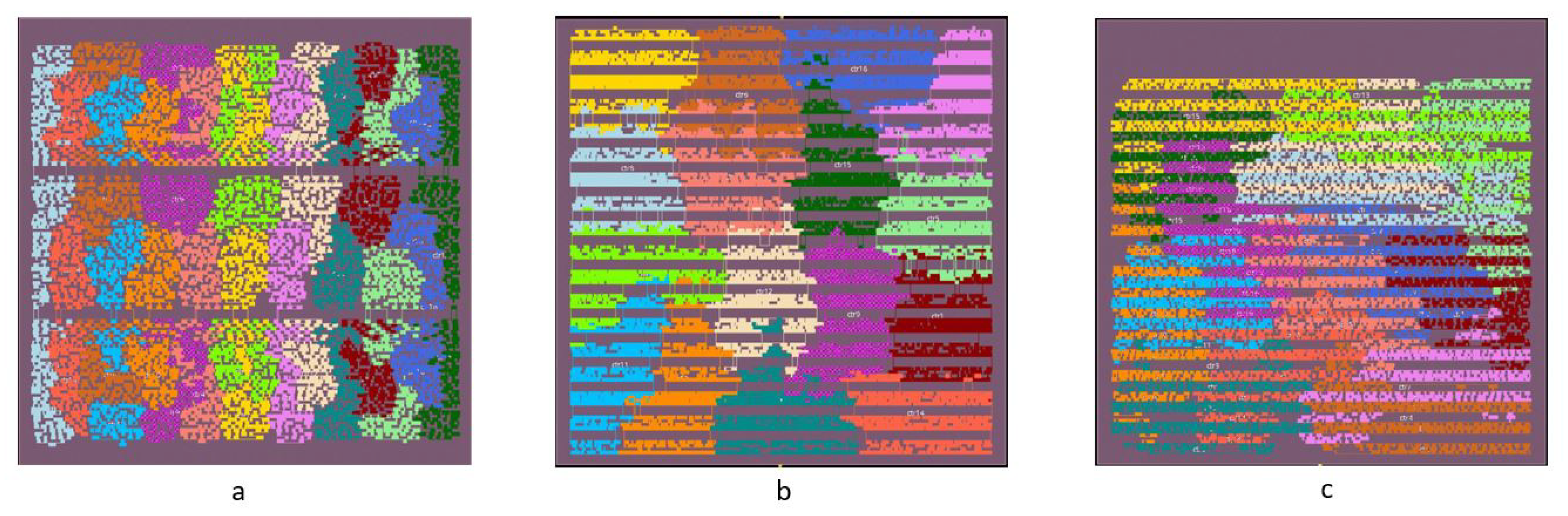
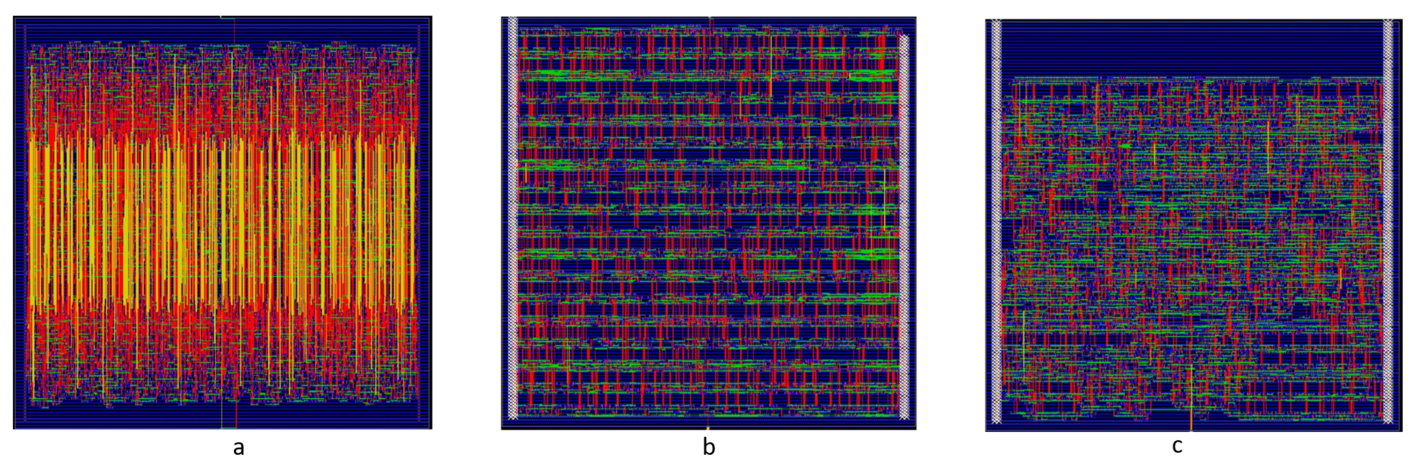
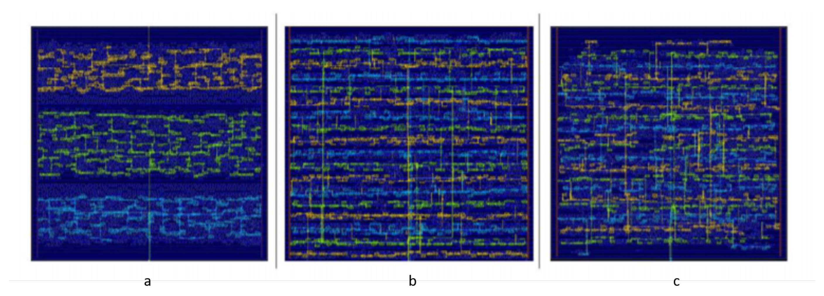
Figure 4 shows the routed designs of 8 × 16 bit counters for the 3 different methods. We did not observe a considerable difference in performance variation for both the interleaved techniques for varying counter dimensions. Compared to the standard 3 block strategy, it is evident that the suggested interleaved and improved interleaved methods result in considerably reduced complexity. In particular, the vertical routing difficulty reduces significantly since the place-and-route tool has more freedom to efficiently place the standard cells closer to each other. Comparing the interleaved and the improved interleaved method, it is clear that the difference between the routing complexity is relatively small, as expected. However the area efficiency (standard cell density) to place the design is improved. The Amouba view of the design is shown on
Figure 5. Each colour represents a triplicated counter. In the 3 block method, the counters are distributed across the 3 bulky blocks. In the interleaved method there is a much better grouping of the counters compared to the 3 block method since the cells can be spaced more closely. Again, the improved interleaved method demonstrates its advantage in the fact that independent combinational path acts as a spacing distance for the other, ensuring maximal area efficiency.
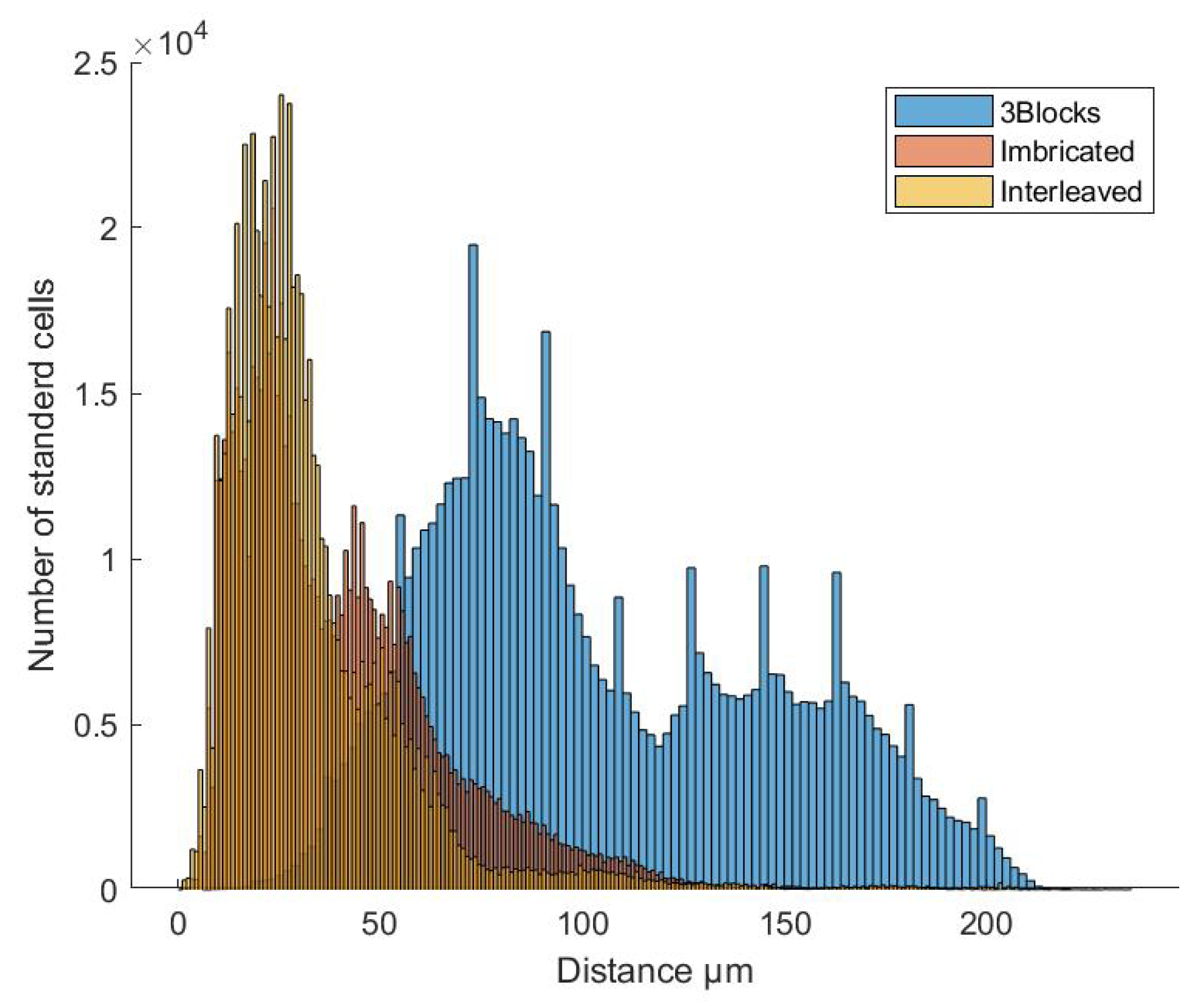
The distances between the cells of same TMR branches are shown on
Figure 6. The Distances between the cells of the 3 block implementations are substantially larger than those within both the interleaved methods. Most cells are spaced within a range of 45
m, which corresponds to approximately 3 elementary, vertical interleaved banks. It is evident from this consequence that the placement engine has more liberty to put cells closer without compromising the radiation hardness. The average cell distance between A-branch and B-or C-cells for the 3 block technique shows two peaks corresponding with the A-B-C and the A-C distance.
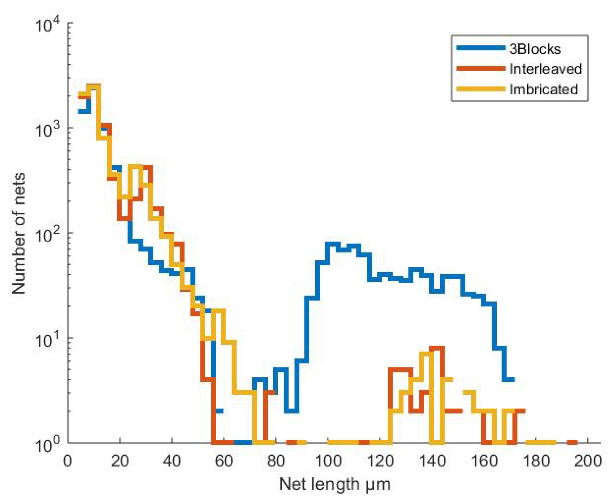
A comparison of the net lengths distribution is shown on
Figure 7. The histogram demonstrates that due to voting interconnections, a significant part of the nets for the 3 block method has 1/3 to 1/2 of the design size. This peak is no longer present in the suggested interleaved techniques. In this case, most networks that are interconnected have a net length of 25
m or less, though this is still design specific. However, in the interleaved model there are still a few long nets. By analysing pre-Clock Tree Synthesis (CTS) and post-CTS histograms, it becomes apparent that these longer connections originate from the clock tree.
Clock trees A-C in the interleaved implementations are now distributed throughout the entire design, while the clock tree was only locally placed in each of the 3 regions in the 3 block approach. This is shown on
Figure 8. Each colour represent one of the clock branches.
The average metal density of the different metal layers is shown on
Figure 9. M1 and all the horizontal layers show no compelling difference since these layers are not used to to interconnect cells. On the other hand, M2 and M4 shows a significant difference due to routing between voter cells. The density in vertical routing layer M2 is almost reduced by half compared to the 3 block method and there is almost no metal density in layer 4, indicating the significance of the proposed strategies. In metal layer 3 there is a slight increase in density of the proposed method. When comparing the interleaved with the proposed improved implementation, a higher gate density is achieved which, as a result, also increases the local corresponding routing density, mainly in M3. Additionally, In the 3 blocks method the placement blocks are much higher which results in a more favourable vertical distribution. In the interleaved methods there are many more shorter blocks which results in a different placement vertically. However, the main figure is the reduction in extremely long M4 nets across the floorplan.
A comparison of the power consumption of the 8 × 16 bit counter is shown in
Table 1. These numbers were extracted after routing and CTS. The internal power is the power consumption of the unloaded standard cells, switching power is the dynamic power consumption due to the switching of the capacitive loads (cells and nets) and the Total capacitance is the sum of all net and input capacitances of the cells. As can be expected, the internal power does not change significantly since the design remains almost identical and the only difference between all methods arises from different buffers which is only a small fraction of the total internal power consumption. The total net lengths of both interleaved methods are significantly smaller compared to the 3 block approach due to the optimal placement by the place-and-route tools. As a result, the total capacitance of the design reduces proportionally as is the dynamic power consumption. Since the main reduction is a result from avoiding long voters interconnects, the improvements become more significant as the design size increases. Therefore, this technique scales well with larger digital designs.
Finally, these results were extracted by evaluating a 65 nm CMOS technology. This methodology however scales well to smaller CMOS nodes. Firstly, in smaller nodes, designs often become more complex and the need for optimal placement increases significantly. Secondly, smaller nodes become more susceptible to SEEs meaning the proposed methods will be increasingly mandatory. Finally, since routing becomes the strongest contributor to power consumption in deep submicron technologies, the proposed methods will show an increasing improvement as devices scale down.


