Article

Power Supply Platform and Functional Safety Concept Proposals for a Powertrain Transmission Electronic Control Unit

by
Diana Raluca Biba
1,
Mihaela Codruta Ancuti
1,*,
Alexandru Ianovici
2,
Ciprian Sorandaru
1 and
Sorin Musuroi
1
1
Electrical Engineering Department, Faculty of Electrical and Power Engineering, University Politehnica Timisoara, 300223 Timisoara, Romania
2
Continental Automotive, Powertrain Transmission Department, 90411 Nurnberg, Germany
*
Author to whom correspondence should be addressed.
Electronics 2020, 9(10), 1580; https://doi.org/10.3390/electronics9101580
Submission received: 12 May 2020 / Revised: 4 July 2020 / Accepted: 15 September 2020 / Published: 27 September 2020
(This article belongs to the Special Issue Autonomous Vehicles Technology)

Abstract

:
In the last decade, modern vehicles have become very complex, being equipped with embedded electronic systems which include more than a thousand of electronic control units (ECUs). Therefore, it is mandatory to analyze the potential risk of automotive systems failure because it could have a significant impact on humans’ safety. This paper proposes a novel, functional safety concept at the power management level of a system basis chip (SBC), from the development phase to system design. In the presented case, the safety-critical application is represented by a powertrain transmission electronic control unit. A step-by-step design guideline procedure is presented, having as a focus the cost, safety, and performance to obtain a robust, cost-efficient, safe, and reliable design. To prove compliance with the ISO 26262 standard, quantitative worst-case evaluations of the hardware have been done. The assessment results qualify the proposed design with automotive safety integrity levels (ASIL, up to ASIL-D). The main contribution of this paper is to demonstrate how to apply the functional safety concept to a real, safety-critical system by following the proposed design methodology.

1. Introduction

It is well known that automotive integrated circuit packages continue to get smaller, but with more and more integrated functions inside the package. This is also available for the power supply module, which represents one of the main circuits from the electronic control unit (ECU). Usually, in automobiles, this type of power supply module is called the system basis chip (SBC) [1]. It integrates multiple functions besides voltage supplies, such as integrated transceivers for communication interfaces, a high-speed controller area network (CAN), and a local interconnect network (LIN), and supervision features like wake-up logic inputs, watchdogs, reset generators, fail outputs, and interrupt outputs. SBC devices are not new to the market, but their usage was increasing in the last period due to their high levels of integration, performance, and reliability. These advantages make them the perfect solution to limit the design’s costs. The ECU cost is significantly reduced by integrating the discrete components. However, this does not mean that all the components are integrated. Due to the limited power dissipation, some power elements remain discrete like, for example, the power switching transistor modules within the converters.
It is necessary to highlight that not only is the cost targeted, but also the safety and security, which represent special requirements in the automotive industry, especially for powertrain applications where the safety SBC architecture shall support independent monitoring of critical safety parameters. For example, it is an essential function for the energy and power management of the battery management systems, as well as the steering and transmission control in electric and hybrid vehicle applications. In these cases, the SBC shall meet automotive safety integrity level (ASIL) C x, or even higher, ASIL-D, and must be ISO 26262 [2] and IEC 61508 [3] compliant. Therefore, the advanced diagnosis of power management must be combined with the safety of power management and trigger the safe state when it is requested by the system.
In a typical transmission control unit (TCU) application, the microcontroller represents the master and controls the SBC (the slave) through a serial peripheral interface (SPI). Safe operation is ensured by the capability of the microcontroller to detect faults using the integrated function of the SBC, called the question and answer (Q&A) watchdog. When detecting possible SBC faults by the integrated function control unit, multiple diagnostics like over–under voltage or over temperature are expected to be made.
To meet the powertrain requirements in terms of cost and safety, a suitable SBC can be FS65xx from NXP [4]. The flexible and scalable NXP SBCs complement the powertrain microcontroller platforms that require functional safety. With buck–boost DC-to-DC architectures that support input voltage ranges from 2.7 V to 60 V for 12- and 24-V markets and scalable power options, these SBCs provide an energy-efficient solution for high-performance microcontrollers [5,6]. The latest Infineon AURIX™ TC3xx microcontrollers are also well suited for safety-critical applications. These microcontrollers combine performance functioning with a powerful safety architecture, which makes them perfectly fitting for powertrain applications. Infineon released its second-generation AURIX™ microcontroller in embedded flash 40 nm technology. It provides increased performance, memory size, connectivity, and more scalability to address the new automotive trends and challenges. In terms of performance, the highest product, TC39x, can have up to six cores running at 300 MHz and up to 6.9 MB of embedded RAM and has embedded voltage regulators. The total power consumption is below 2 W [7,8].
For hardware engineers, designing and optimizing safety supplies has become a mandatory task. Unfortunately, this task is often time-consuming and technically challenging. To simplify the design tasks and improve design quality and engineer productivity (i.e., to become more agile), this paper describes in detail, as a procedure, the design steps of a power supply concept for safety-critical application [9,10]. The proposed methodology represents a specific, but very well-organized guide to transmission control unit function, and it can be easily extended to other safety-relevant applications. The design procedure has as its focus cost, safety, and performance to obtain a robust, cost-efficient, safe, and reliable supply design.
The paper is organized as follows. Section 2 discusses design challenges related to safety operation for a novel concept of a safety-relevant power supply with only 5 V for the main component from an ECU, the microcontroller. In order to prevent and limit design difficulties and challenges, a design flow procedure is proposed in Section 3. In Section 4, special attention is paid to getting proper values of the 5 V regulator components by analyzing the SBC and microcontroller requirements, in terms of safety supply. The selection of components is proved by performing worst-case analysis to accomplish the hardware robustness target. Section 5 deals with the enhanced features of the microcontroller and power SBC, in terms of power management, to guarantee a safe state by switching off the entire system in case of supply faults. Accordingly, a complete safety switch off path (SWOP) circuit is proposed for a printed circuit board (PCB) schematic. Finally, Section 6 draws conclusions and proposes future research work.

2. Design Challenges

There are three questions which represent the starting point of the proposed design:
  • What is needed (simplest solution) to supply the TC3xx with power from the FS65xx SBC to fulfill ASIL-D? How are the 3.3 V and 1.3 V internally generated by the TC3xx?
  • What happens (over a lifetime) with the TC3xx if the power supply from the SBC is made as described in the datasheet?
  • How will the overall safety concept look?
The proposed power supply concept is to have an SBC, which is delivering only 5 V to microcontroller. The 3.3 V and 1.3 V signals are internally generated by the microcontroller itself by using its embedded voltage regulators, as can be seen in Figure 1. By using this concept, two major advantages can be derived: (1) reducing the use of external components, which automatically involves a price reduction for the electrical bill of material (eBOM) and PCB space [11], and (2) avoid electromagnetic interference (EMI) noise emissions; EMI requirements are an important demand to be fulfilled within transmission applications. By reducing the external 3.3 V supply, this eliminates a potential EMI noise emission [12].
For the SBC, the pre-regulator (VPRE) is configured to be a non-inverting, buck–boost type DC-to-DC converter, and the core output (VCORE) is configured to incorporate a buck topology. A linear topology is also available, but in the current case, the scope is to minimize energy consumption through the DC-to-DC switching regulator. The VCORE is 5 V, representing the main supply for the microcontroller. It also supplies other safety-relevant circuits. The total current consumption was calculated and considered at a maximum value of 1.5 A. For communication, a physical interface with integrated CAN FD and LIN transceivers was chosen. A long duration timer (LDT) was enabled to check the SBC in power off mode. As can be seen in Figure 2, the ordering code of the SBC component is MC33FS6512LAE/R2 [13,14,15].
For the microcontroller, the second generation of the Infineon AURIX family, the TC397 microcontroller, is considered. The ordering code for the microcontroller is SAK-TC397TP-64F200N. This nomenclature, as shown in Figure 3, corresponds to a production device with a temperature range from −40 °C up to 125 °C, with board assembly recommendations (BGA) package 292, which consumes below 2 W, a triple core running at 200 MHz, support for floating and fixed-point operations, a 4 MB flash size, and CAN FD communication [16].

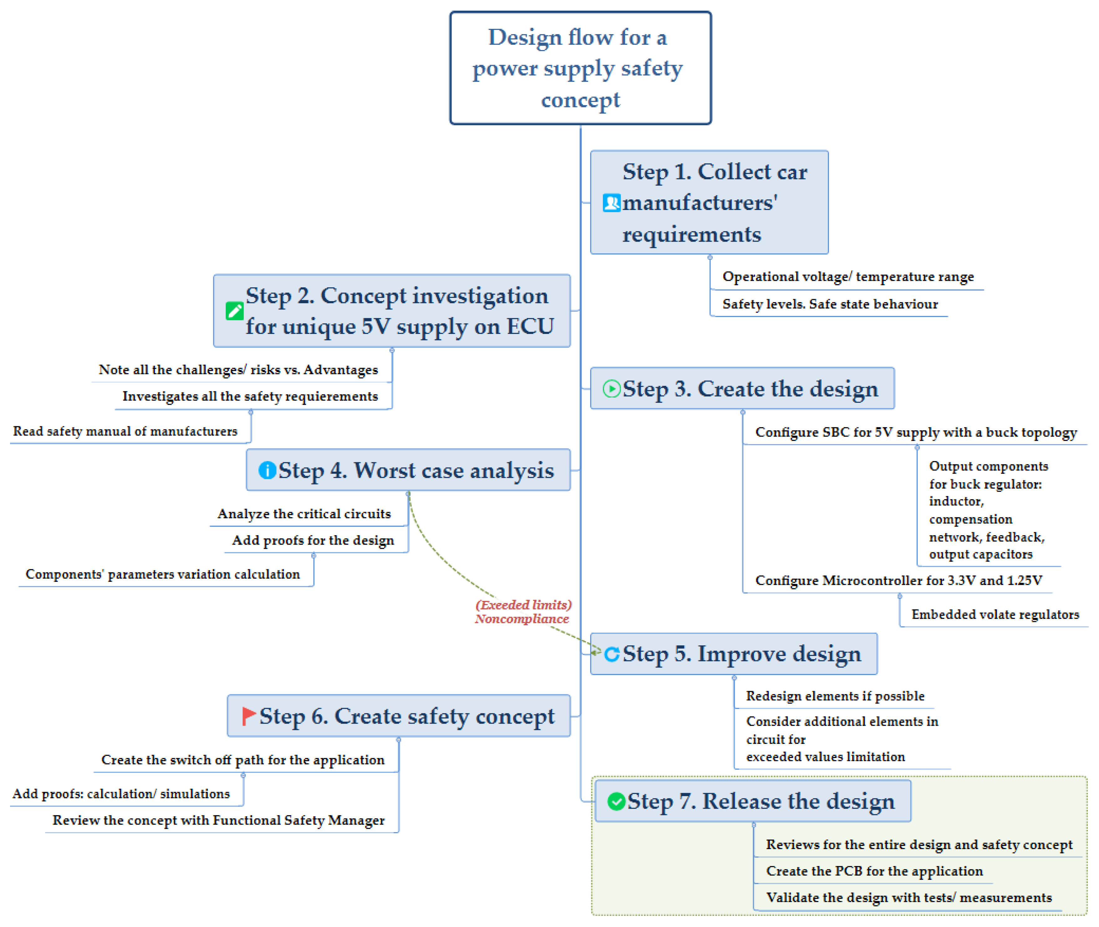
3. Design Flow Proposal

The design of safety power supplies requires significant attention to detail. A simplified procedure is proposed by using an Xmind tool to map all the mandatory steps, as can be seen in Figure 4. As can be seen, safety is the word dominating the entire flow. The design must start from the vehicle’s original equipment manufacturer’s (OEM) requirements in terms of safety because a critical application shall support and enable the safety function. For a typical automotive application, it is mandatory to start from the OEM’s safety requirements to take active measures to achieve the required risk reduction in the sphere of active safety. For example, for a TCU application for a double-clutch automated transmission, the safe state reaction is to disable the functions of the actuators (putting in break mode the brushless DC motors). For the airbag control unit (ACU), the safety reaction is the opposite, and it shall enable the actuators. Therefore, Step 1 is important to define the safety measures to be taken for the applications.
The safety mechanism shall be carefully analyzed from both cost and effectiveness points of view. Therefore, in Step 2, the designers shall put on paper a proposed configuration for a proper supply concept. It represents the time for noting all the challenges, advantages, and risks. Then, based on these assumptions, the design will be created, taking into consideration the components’ specifications and safety recommendations. In order to check and prove that all the delivered voltages are within the desired range, a worst-case analysis (WCA) shall be performed, as listed in Step 4. For functional safety management (FSM), the WCA represents a safety metric through design and implementation. If the WCA shows that monitoring is not ensured, major changes shall be considered in the design. Usually, there are two options: adding an extra circuit for monitoring or reconsidering components which may have better performance. Only after the design is improved, in order to have good coverage of the fault’s detection, shall the safety concept be released (Step 6). In the switch off or on path safety concept, all the safety activation signals are considered in redundant logic. After a final review, the design can be completely released.

4. Power Supply Design and Safety Requirements Evaluation

The focus of this section is to provide a correct and robust SBC design which will withstand the automotive requirements, in terms of safety. This paper will break the procedure down into a step-by-step action that every designer can follow to create a proper safety circuit between the supply and microcontroller in safety-relevant applications.

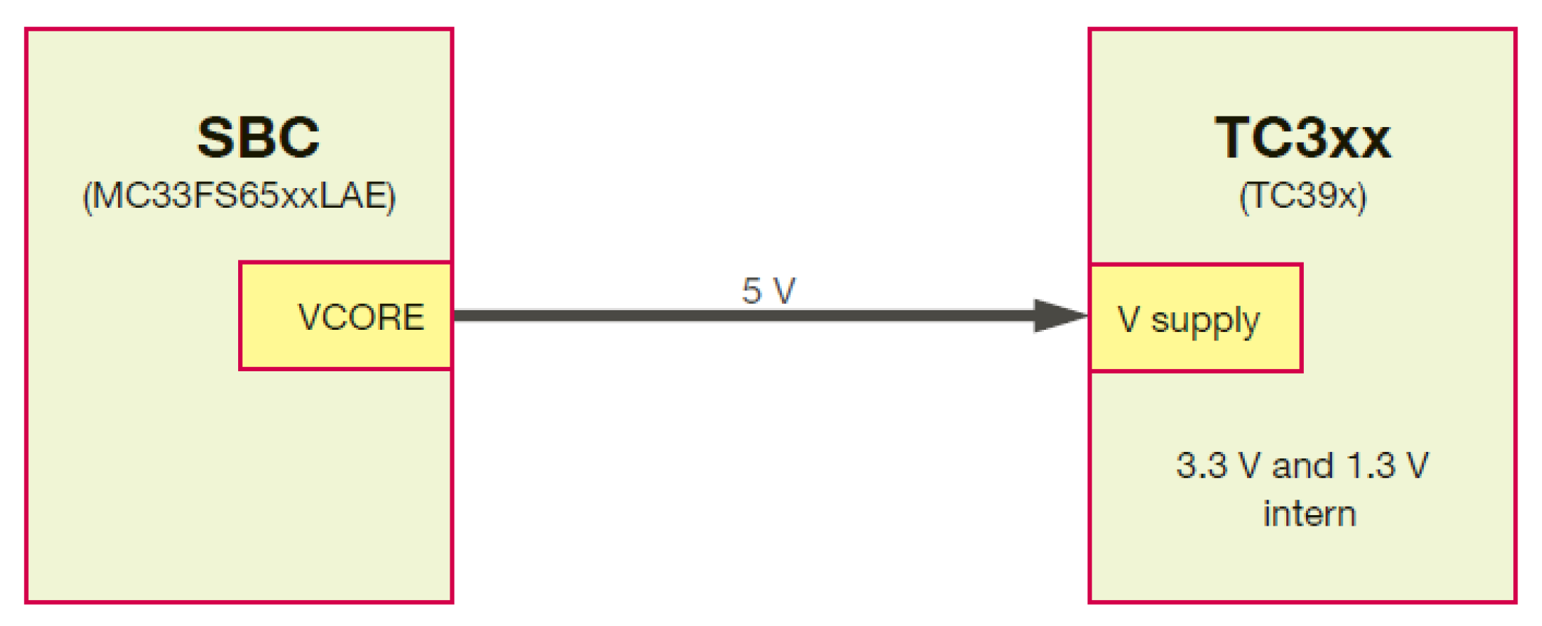
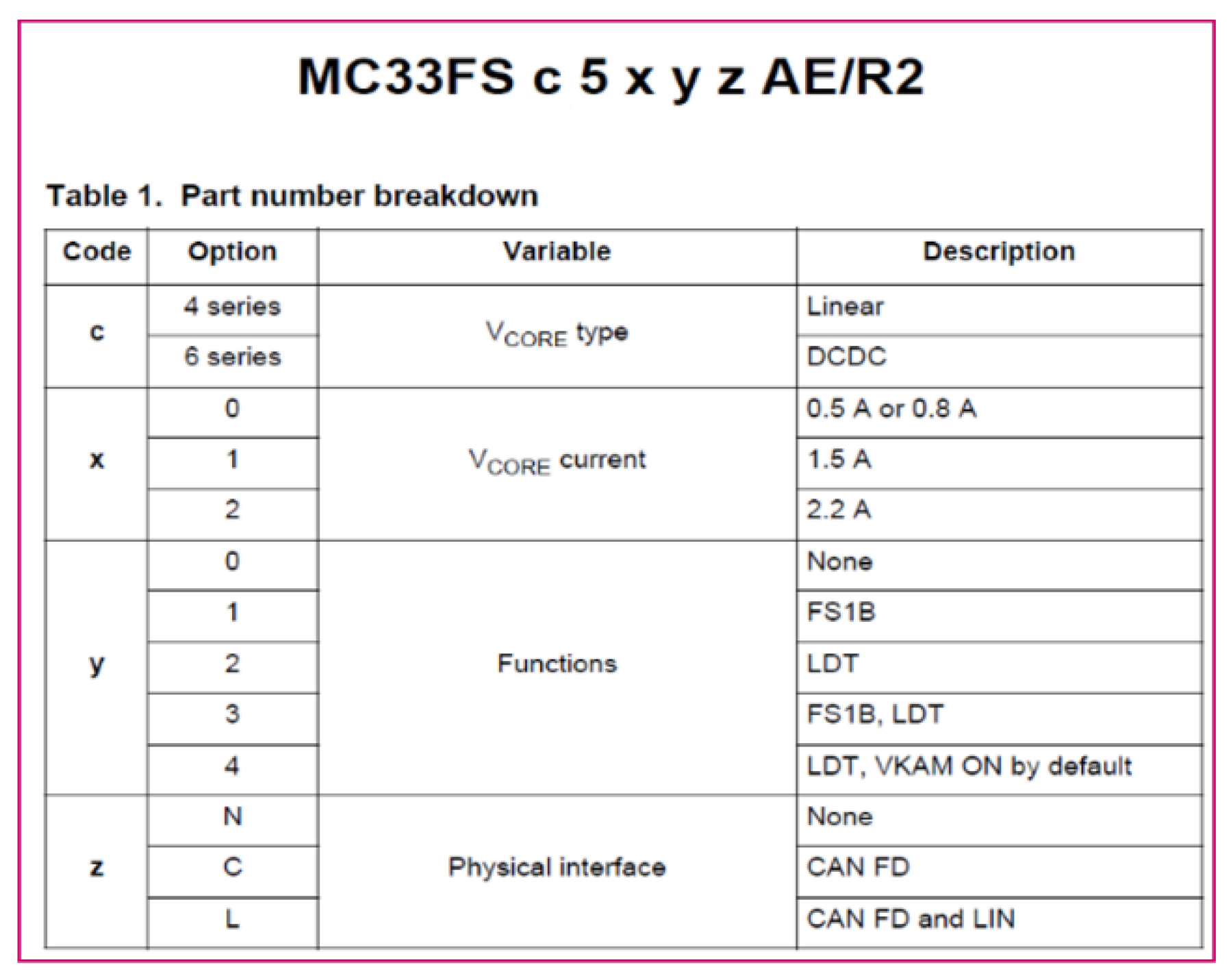
4.1. What Is Needed (Simplest Solution) to Supply the TC397 with Power from FS6512 SBC to Fulfill ASIL-D?

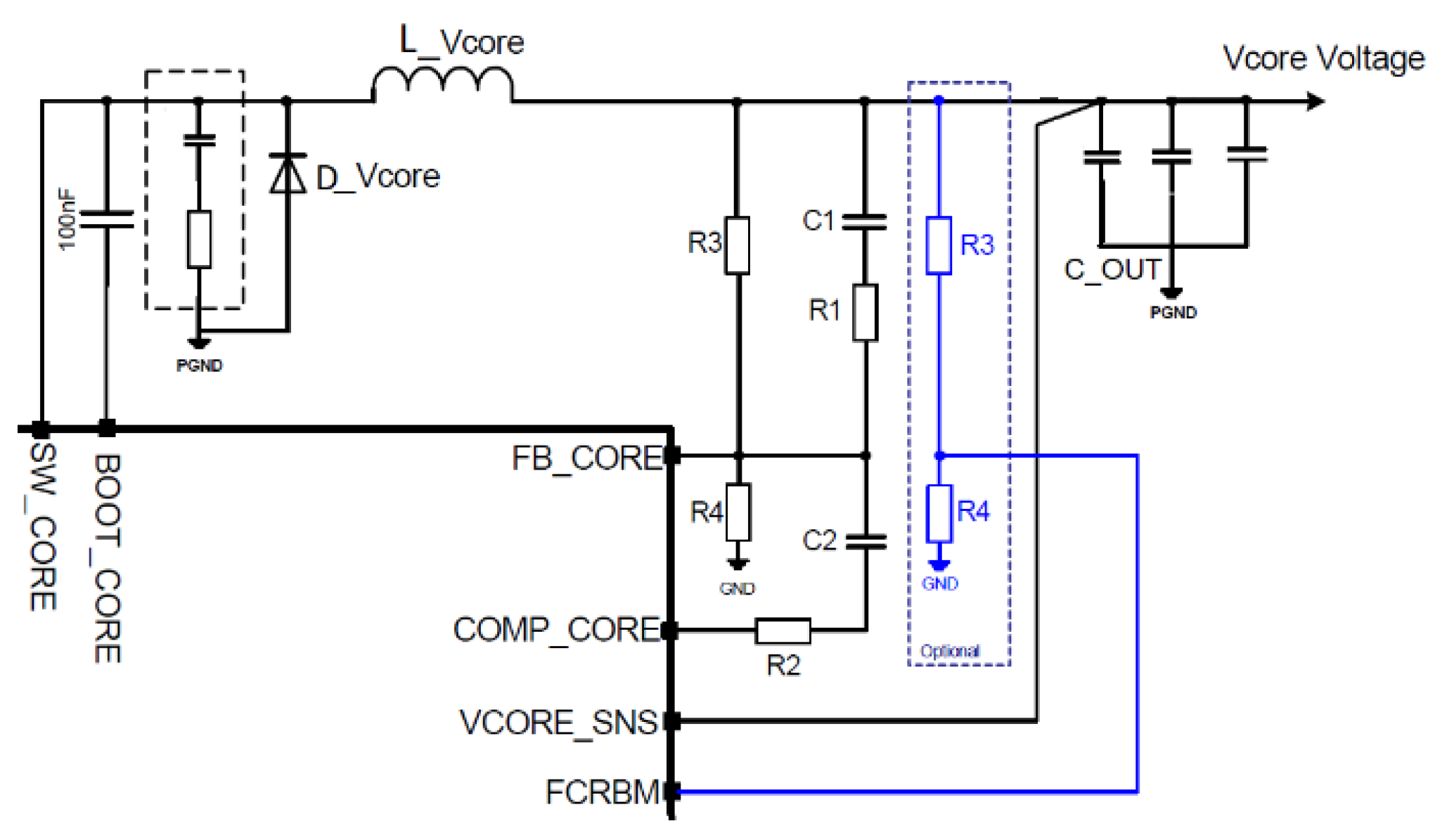
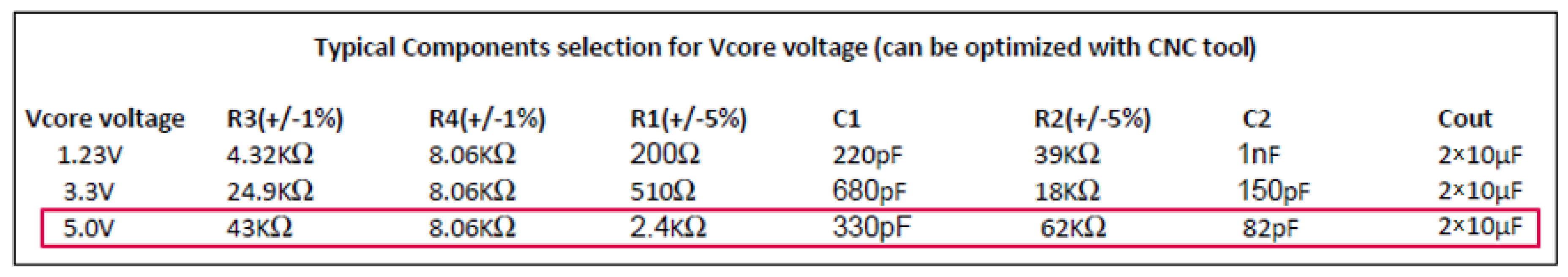
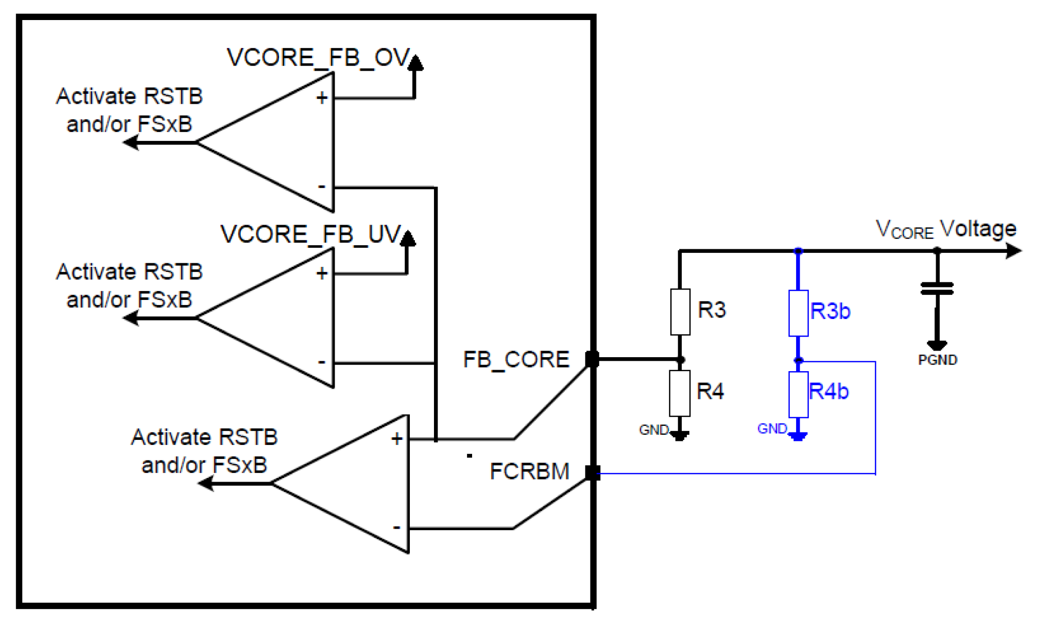
4.1.1. V Configuration of FS6512: For VCORE—BUCK Regulator

The FS6512 VCORE regulator is a buck DC–DC topology, operating in voltage control mode. The high side of the switching transistor is connected to the VPRE and is integrated into the SBC. The VCORE buck regulator shall regulate the output voltage only against the output loading. In this case, the input variations are stable. The typical switching frequency is fixed at 2.4 MHz. The VCORE buck accomplishes proper regulation within the feedback loop by integrating an error amplified by linear feedback. The output voltage VCORE is configurable in a range from 1 V up to 5 V through an external resistor bridge (R3/R4), as can be seen in Figure 5. Therefore, it is necessary to adjust the divider values to get 5 V. The first divider is connected between the VCORE and the FB_CORE feedback pin. VCORE = VCORE_FB ((R3 + R4)/R4). For safety purposes, to meet ASIL-D requirements, a second feedback monitor can be used to monitor redundantly the VCORE voltage, having the feedback loop connected to the FCRBM (feedback core resistor bridge monitoring) pin. If not used, the pin is connected directly to the FB_CORE. The safety manual recommends using less than 1.0% accuracy resistors, setting R4 = 8.06 kΩ, and adjusting R3 to obtain a VCORE of 5 V. The component datasheet provides a voltage accuracy of ±2.0% (without considering the accuracy of the external resistors). The stability of the overall converter is ensured only by using an external compensation network (R1/C1/R2/C2) connected to the COMP_CORE pin.
Usually, the components’ datasheets tell only one part of the story and recommend generic (typical) values for the components, as can be seen in Figure 6. It is necessary to highlight that when working with safety-critical design, all hardware designers shall add proofs for the design and not take the manufacturer’s stated output capabilities for granted. Therefore, in this paper, for the proposed concept, the authors added proofs and considered a worst-case scenario for buck inductor (LCORE) and compensation network (R1/C1/R2/C2) selection. The component selection must be done in such a way that the SBC should provide output voltage (output power) with some safety margin on top, in terms of stability.
In order to design the VCORE for 5 V, the LCORE inductor was calculated. A correct inductor selection is mandatory for proper design because the inductor has an impact on the efficiency, on the transient response, and on control loop stability. A poor inductor selection can cause damage to the converter, lead to premature overcurrent protection, and limit output capability. The inductor was sized so as to avoid saturation and help the VCORE converter remain in continuous current mode (CCM) through this range, considering the worst-case limits. The calculation of the minimum inductor value (Lbuck_min) was performed using a Mathcad tool. The following formula was used:
L buck _ min ( V in max V out rated V R ds _ on max ) Duty _ Cycle 2 I L min min f sw min
where the following parameters were considered: Vin = VPRE (the pre-regulator input voltage); Vout = VCORE, the output current through inductor (IL); fsw, the converter switching frequency; and VRds_on (implicitly, the voltage across the switching element).
The duty cycle was computed as depicted by the below equation, considering the voltage drops through the switching element and across the diode (Vf_diode):
Duty _ Cycle ( V out rated + V f _ diode max V in max V R ds _ on max )
The minimum current through the inductor (ILmin) was calculated as shown below:
Δ I L kI out max I L min Δ I L 2
where k is the inductor ripple current factor (20–40%) applied to the maximum allowed output current ( I out max ).
By running the above calculation, a minimum value of 2.118 µH was obtained for the buck coil, which corresponds to a 2.2 µH standard value.
Taking into consideration this coil value, the maximum output current of 1.5 A, the 5 V output voltage, and by using the Graphical User Interface (GUI) provided by NXP to check the converter stability, plots for transient and Bode characteristics were evaluated in order to obtain the right values from the compensation network. Considering the following values—C1 = 330 pF, R1 = 1.1 kΩ, C2 = 100 pF, R2 = 47 kΩ—it can be stated that the control loop was properly compensated. Figure 7 shows a simulated Bode plot with a sufficient phase margin around 55 °C and a gain margin of −20 dB.

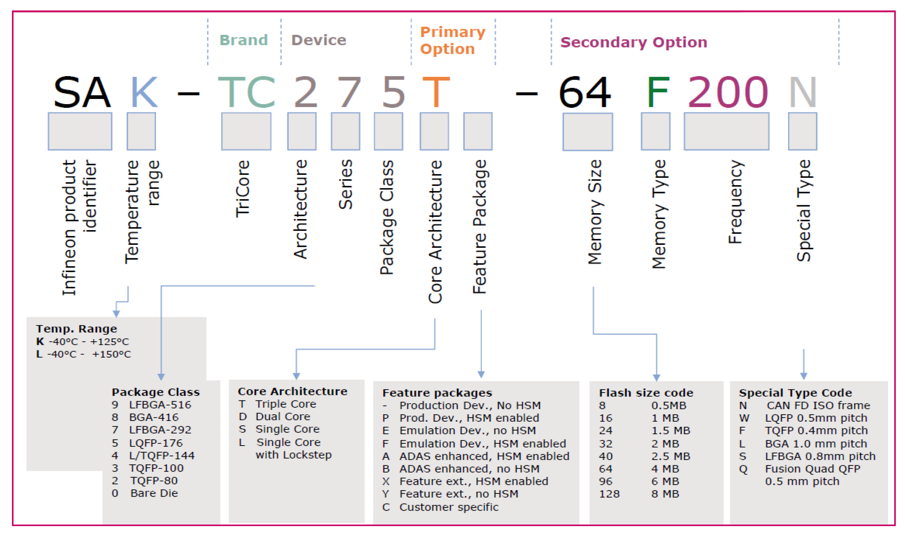
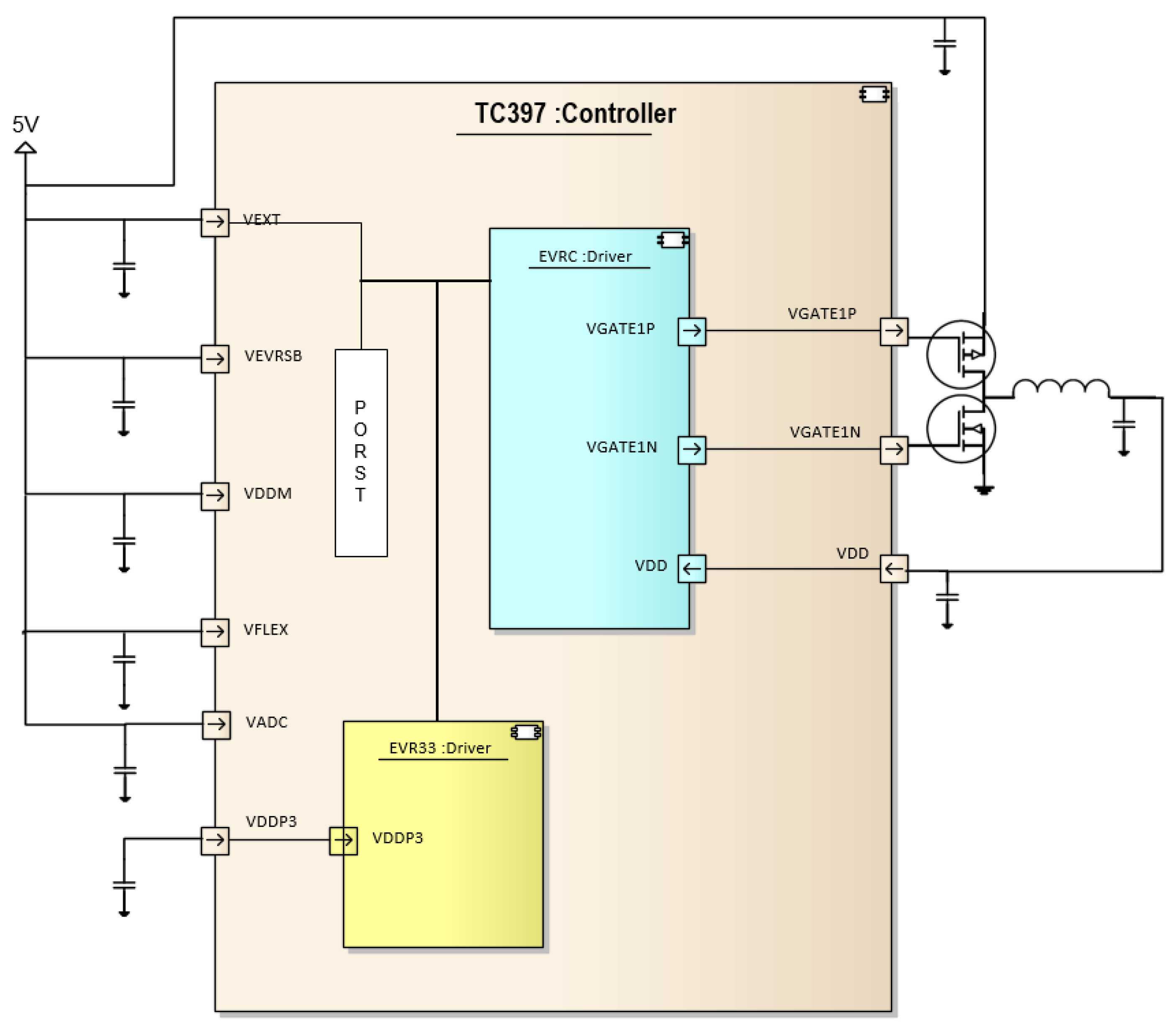
4.1.2. V Configuration Supply Concept for TC397

The 5 V signal provided by the SBC is the unique supply of the microcontroller, as can also be seen in Figure 8. It directly supplies the embedded voltage regulators for core and flash supply (EVRC and EVR33). It supplies the analog ports (VDDM and VADC), the flexible ports (VFLEX, configured to be supplied from 5 V and not from 3.3 V), and the embedded voltage regulator in standby mode (ERVRSB). It is important to mention that the supply mode selection is done in an external hardware configuration. The microcontroller contains dedicated pins called HWCFG_x for this purpose. At the HWCFG_1 pin, corresponding to port P14.5, EVR33 is enabled or disabled at startup. At the HWCFG_2 pin, corresponding to port P14.2, EVRC is enabled or disabled at startup. The enabled function is selected in this design by adding pull-up resistors externally in order to have a logic 1 on the input ports.
The EVRC (embedded voltage regulator for core supply) regulator was implemented as a switched mode power supply regulator (buck topology), generating the core supply VDD (the label of the power suplly) of 1.25 V. This step-down (VDD) contained not only the integrated voltage regulator, but the voltage feedback loop too. Due to power loss limitation, the switching elements (the N channel and P channel of the MOSFETs (Metal-Oxide Semiconductor Field-Effect Transistor)) and the LC (an electric circuit consisting of an inductor and a capacitor) filter were considered externally. For the schematic, in order to minimize the PCB space, Infineon BSZ215C H components—complementary power MOSFETs—were used, with both N- and P-channel MOSFETs within the same package. For the filter, due to the resonance frequency of 3.6 MHz, the coil value was 3.3 µH (Vishay—IHLP1616BZ-ER-3R3-M-5A) and the output capacitor value was 22 µF (ceramic capacitor 22 µF, TDK − CGA6P1 × 7R1C226KT).
The EVR33 regulator represented the embedded voltage regulator for the 3.3 V voltage supply. It was always implemented as an LDO (Low Dropout) regulator and generated a digital supply for Flash (VDDP3) of 3.3 V (with internal pass devices). It contains an integrated voltage regulator, a pass device control unit, and a voltage feedback loop. Only the output capacitor (ceramic capacitor 100 nF, TDK—CGA3E2X7R1H104KT0Y9N) is not integrated.

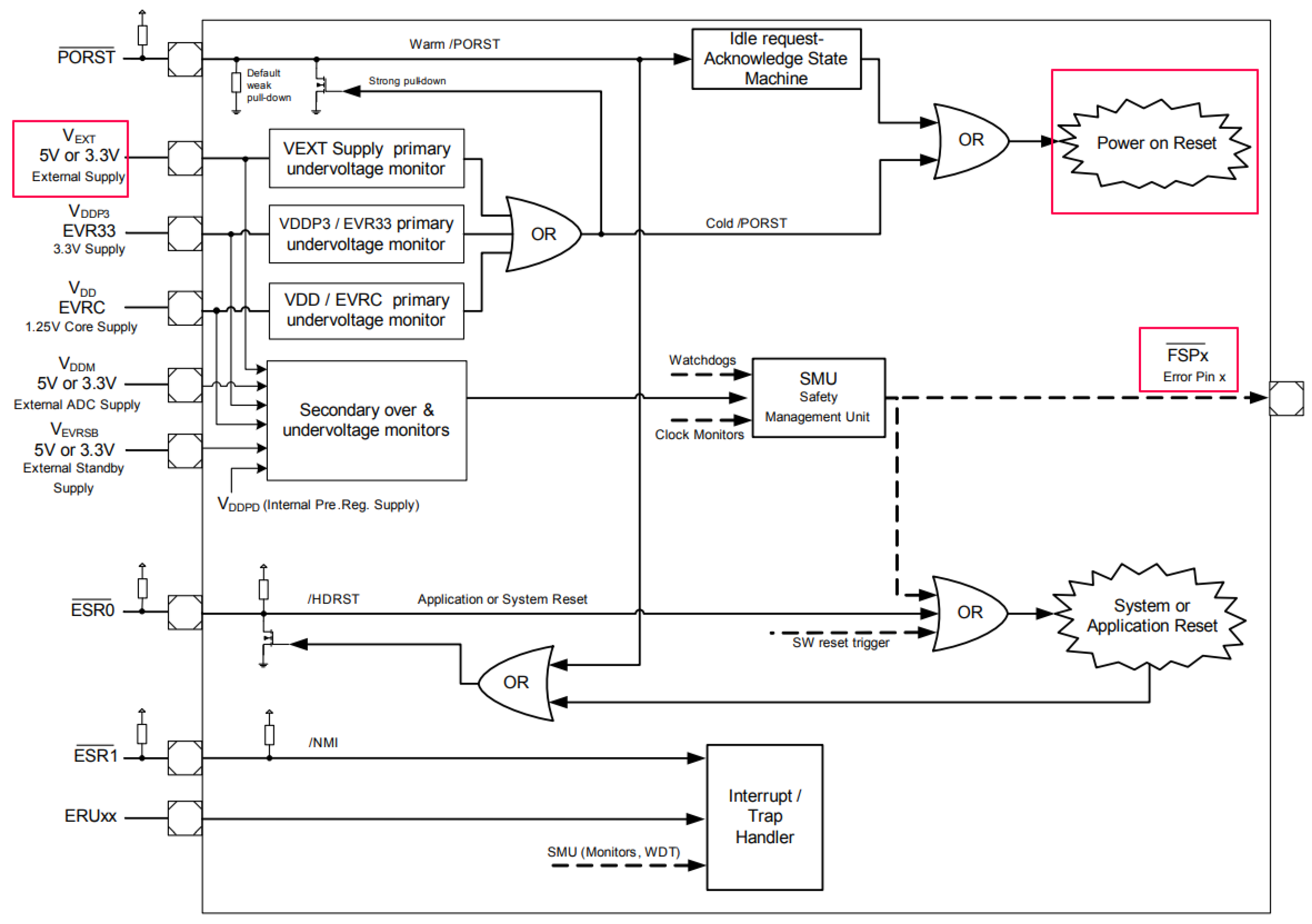
4.2. What Happens (over Lifetime) with the TC3xx If the Power Supply from PSBC Is Done Like in the Data Sheet?

The design for the power supply was completed by delivering 5 V to the microcontroller with a VCORE buck and to its proper selected components. The supply structure for the controller was completed by choosing suitable output components. It was not enough. This section highlights that a deeper investigation is necessary by looking for the worst-case scenario. The worst-case analysis for the design is a proof that the hardware meets or exceeds the design specifications for its lifetime. For a safety application like the TCU, the WCA is mandatory to be performed; it is not an option. The designers can foresee potential damages of the design, predict the lifetime decreasing and, in addition, anticipate the predictable faults in the system (SBC microcontroller). In other words, designers can reduce financial, legal, and safety risks and help to ensure satisfactory performance for the application.

4.2.1. TC397 Microcontroller Requirements in Terms of Supply

An important step in the design is to check the remaining useful life of the microcontroller when the SBC exceeds 5 V, which is the rated voltage. Verification is needed in order to get a precise understanding of the worst-case behavior of the TCU. The 5 V signal provided by the SBC shall match the microcontroller specification regarding quality, robustness, lifespan, and safety goals. The microcontroller requirements, in terms of supply voltage range, are depicted in Table 1 below.
Normal functioning is ensured between 4.5 V (corresponding to a −10% tolerance) and 5.3 V (corresponding only to a 6% voltage tolerance). This is the reason for the SBC supply main limitation. A larger margin for an overvoltage condition of at least +10% was expected. In this case, it means that the SBC must trigger the safety case when the VCORE already exceeds 5.3 V. In addition, as it is listed in the table, the microcontroller will still operate without resetting, but in safety cases up to 5.6 V for 100 h, or up to 6.5 V for 10 h. In addition to that, during the reset mode, it can handle 6.5 V for a maximum of 60 h. The operation hours are given by the microcontroller manufacturer based on lifetime measurements of a large number of components within its structure. From the designers’ points of view, the results obtained are trustworthy, but in the automotive domain, proofs are needed. For the current technology, there is no possibility to measure the lifetime reduction (counting the remaining hours before damage) in an overvoltage situation, but only to predict it. In addition, in a safety-critical operation case, it is more crucial. The risks come when the hours listed in the table are not reflecting reality. No one will take such risks in the context of damaging the master component of the TCU in ASIL-C or D applications. The safety shall be triggered at 5.3 V and stop the TCU system’s operation. This means that the FS6512 SBC shall detect the overvoltage at 5.3 V and generate the safety at the FS0B pin. FS0B represents the first output of the safety block (active low signal type). For this action, the designers shall demonstrate by calculation the safety activation at 5.3 V. Only by calculation can the designers identify the design issues and the alternatives or get confidence in a good critical design.

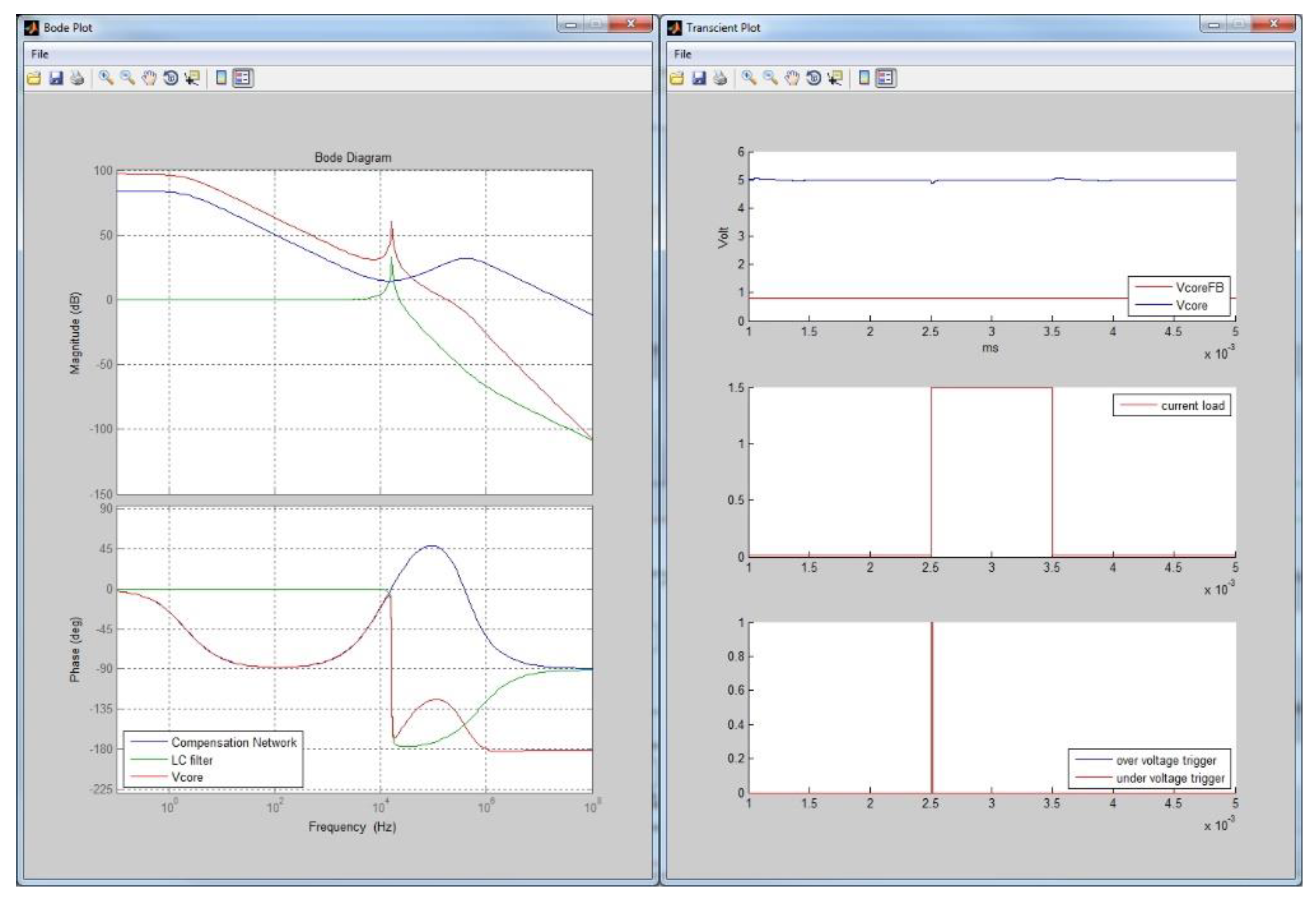
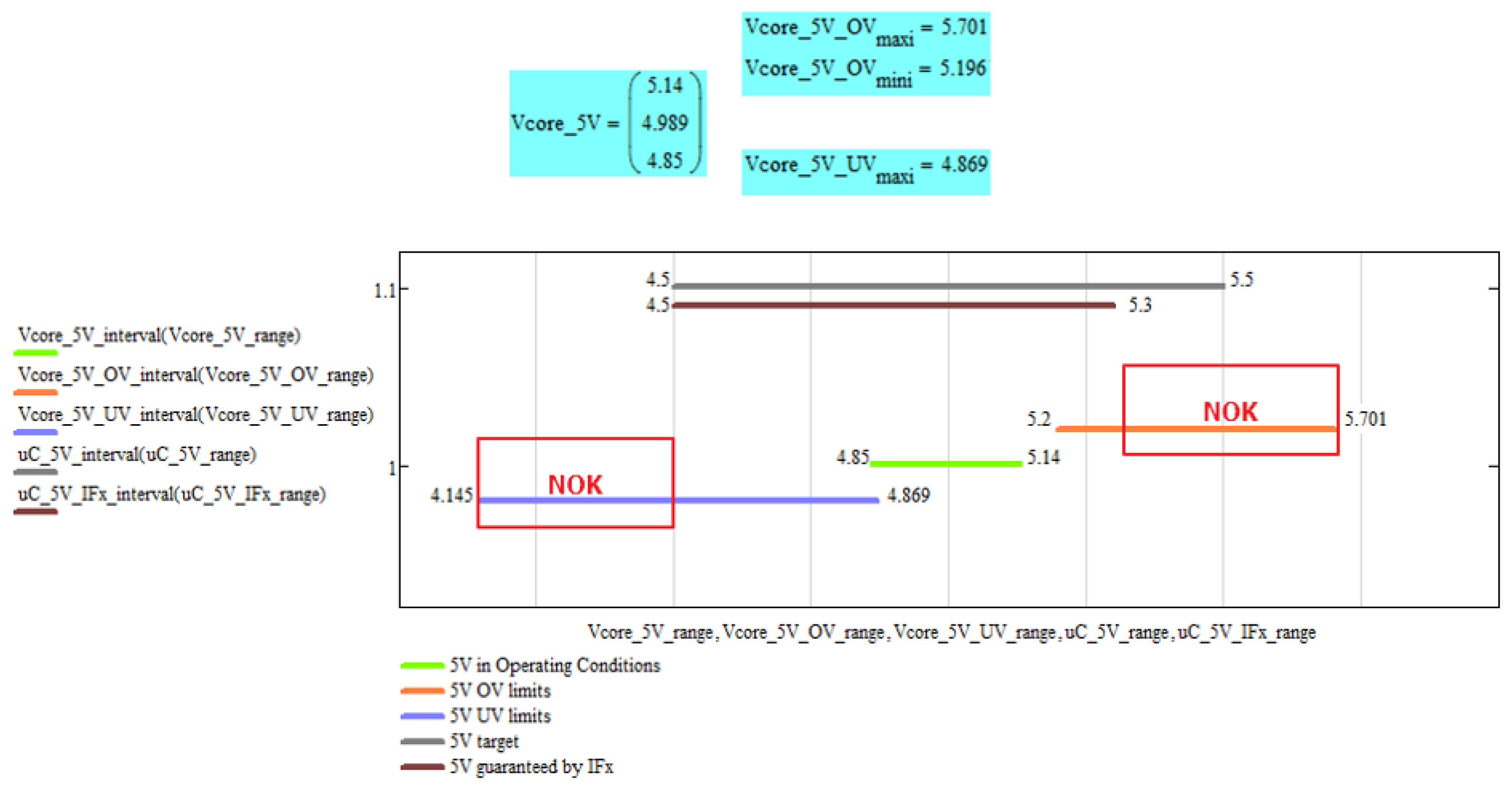
4.2.2. VCORE 5 V Worst-Case Mathcad Calculation

The computational method used as a validation of overvoltage detection in this paper was the extreme value analysis (EVA) method. The purpose of the calculation is to obtain an accurate indication of the worst-case results, especially for the overvoltage detection range. Along the calculation process, all the electronic components’ tolerances were considered, including initial manufacturing tolerances, environmental (temperature) tolerances, aging tolerances, detraction, and drift factors.
A WCA was then performed, using a Mathcad tool, for the VCORE circuit by setting all the components’ values to their end tolerance limits. For the feedback resistors (R3, R4) in the calculation process, 0.1% initial tolerance, 0.25% aging tolerance, and a temperature coefficient (temp_coef) of 25 ppm were considered. The formula below was used:
R n ( R , tolerance , ageing , temp _ coeff , t ) [ R ( 1 + tolerance ) ( 1 + ageing ) ( 1 + Δ Temp · temp _ coeff ) R R ( 1 tolerance ) ( 1 ageing ) ( 1 Δ Temp · temp _ coeff ) ]
where ∆Temp is the difference between the application’s maximum temperature (125 °C) and its rated temperature (25 °C). The following results were obtained:
R 3 = ( 42.454 × 10 3 42.2 × 10 3 42.052 × 10 3 ) ;   R 4 = ( 8.108 × 10 3 8.06 × 10 3 8.012 × 10 3 ) .
The maximum, rated, and minimum VCORE computed values are in correlation with the feedback directional sensitivity circuit of the FS6152 supply (VCORE_FB). Therefore, the undervoltage and overvoltage feedback values (VCORE_FB_UV; VCORE_FB_OV) were extracted from the manufacturer specification and introduced in a Mathcad tool as listed in the below formula:
V CORE _ FB = ( 0.816 0.8 0.784 ) ; V CORE _ FB _ UV max = 0.773 ; V CORE _ FB _ OV max = 0.905 ; V CORE _ FB _ UV min = 0.67 ; V CORE _ FB _ OV min = 0.84 .
For the rated VCORE obtained using (6), the rated range will be
V CORE _ 5 V ( V CORE _ FB max R 3 max + R 4 min R 4 min V CORE _ FB rated R 3 rated + R 4 rated R 4 rated V CORE _ FB min R 3 min + R 4 max R 4 max ) ;   V CORE _ 5 V = ( 5.14 4.989 4.85 ) .
For the overvoltage detection range (VCORE_5V_OV), the VCORE limit will be
V CORE _ 5 V _ OV max V CORE _ FB _ OV max R 3 max + R 4 min R 4 min ;   V CORE _ 5 V _ OV max = 5.701 ; V CORE _ 5 V _ OV min V CORE _ FB _ OV min R 3 min + R 4 max R 4 max ;   V CORE _ 5 V _ OV min = 5.196 .
For the undervoltage detection range (VCORE_5V_UV), the VCORE limit will be
V CORE _ 5 V _ UV max V CORE _ FB _ UV max R 3 max + R 4 min R 4 min ;   V CORE _ 5 V _ UV max = 4.869 ; V CORE _ 5 V _ U V min V CORE _ FB _ UV min R 3 min + R 4 max R 4 max ;   V CORE _ 5 V _ UV min = 4.145 .
The results of the above calculus represent, basically, the best approach to predict the under and overvoltage 5 V supply faults in the circuit. As can be derived from Figure 9, the normal operation is ensured within the range of 4.85–5.15 V. The main drawback occurs in the detection range of the undervoltage and overvoltage monitored behaviors. From the plot in Figure 9, it can be seen that the detection is significantly out of range. In the case of undervoltage detection, a power-on reset can be generated. The critical point represents overvoltage detection when the microcontroller could be damaged completely. From this moment, it is clear that the design needs improvements in order to operate properly and safely. There are two options, and the first one is to use components with better performance. However, in this case, 0.1% resistors were already used, despite the fact that the SBC manufacturer specifies 1%. The remaining option is to add to the design a specific circuit which could limit or switch off operation when the VCORE voltage goes higher than 5.3 V. A proposed voltage supervisor component is TPS3702-DX50Q1. It generates a safe state activation or reset when the voltage is higher than 5.3 V.

5. Power Supply Safety Concept Design Proposal

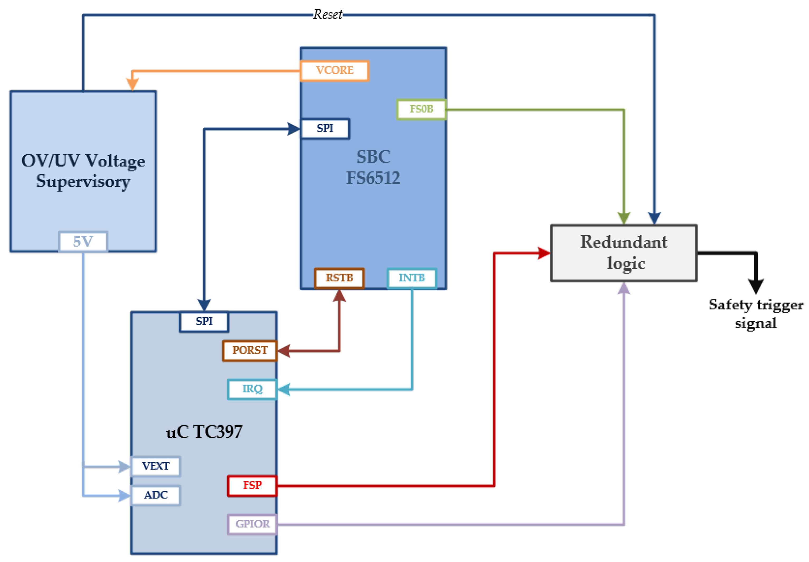
5.1. Safety Connections

The selection of the best safety mechanism, as listed in this paper, will be a tradeoff between performance and cost. Because improved detection cannot be done from the components point of view, an additional circuit will be considered and, thus, the total cost of the application will increase. This additional cost cannot be avoided, because the statement of safety first prevails. The effort made for the design to meet safety constraints is moved now into design efforts to create a proper interconnection switch-off path for the TCU considering all the three blocks: the microcontroller, the SBC, and the overvoltage and undervoltage monitoring circuit. This section provides a good safety activation concept, looking step by step at safety activation signal configuration for each main block.

5.1.1. Check the SBC Safety Activation

The FS6512 SBC plays an important role in safety-oriented TCU system partitioning. A dedicated fail-safe state machine is implemented to bring and maintain the TCU application into a safe state. The SBC provides an overvoltage and undervoltage monitoring feature of the FB_CORE, which is part of the fail-safe state machine, as can be seen in Figure 10.
If the FB_CORE is above or below the value specified by the SBC datasheet, RSTB (the reset pin) and/or FS0B (depending on the device configuration) are asserted as low. The reset pin controls and monitors the microcontroller’s reset pin. The FS0B is available to control or deactivate any fail-safe circuitry in redundancy with the microcontroller. Both RSTB and FS0B shall be integrated in the switch-off concept. In addition, FS6512 has an interrupt output pin, called the INTB pin, for error information, connected at the microcontroller’s non-maskable interrupt interface.

5.1.2. Check the µC Safety Activation

In order to fulfill technical safety requirements, the TC397 microcontroller has a PMS (Power Management Systems, as shown in Figure 11) module, which implements software with staggered voltage monitoring. The PMS is built upon a primary and a secondary monitor, providing adequate redundancy to activate the safe state in case of under or overvoltage faults. The primary monitoring circuit can generate only an undervoltage detection for the following voltages: 5 V, 3.3 V, and 1.25 V. In case of undervoltage detection, in the primary monitoring unit of the PMS, a power-on reset will be generated. In the secondary monitoring block, both functions of under and overvoltage protection are implemented. In case of detection in the secondary monitoring unit of the PMS, the SMU (Safety Monitoring Unit) will generate an alarm on the error pin (FSPx, the fail-safe pin). Detection thresholds can be set in the software code via SWDUVVAL/SWDOVVAL bits in the PMS_EVRUVMON/PMS_EVROVMON registers. The signal provided by the microcontroller at the FSP pin shall be part of the switch-off concept.

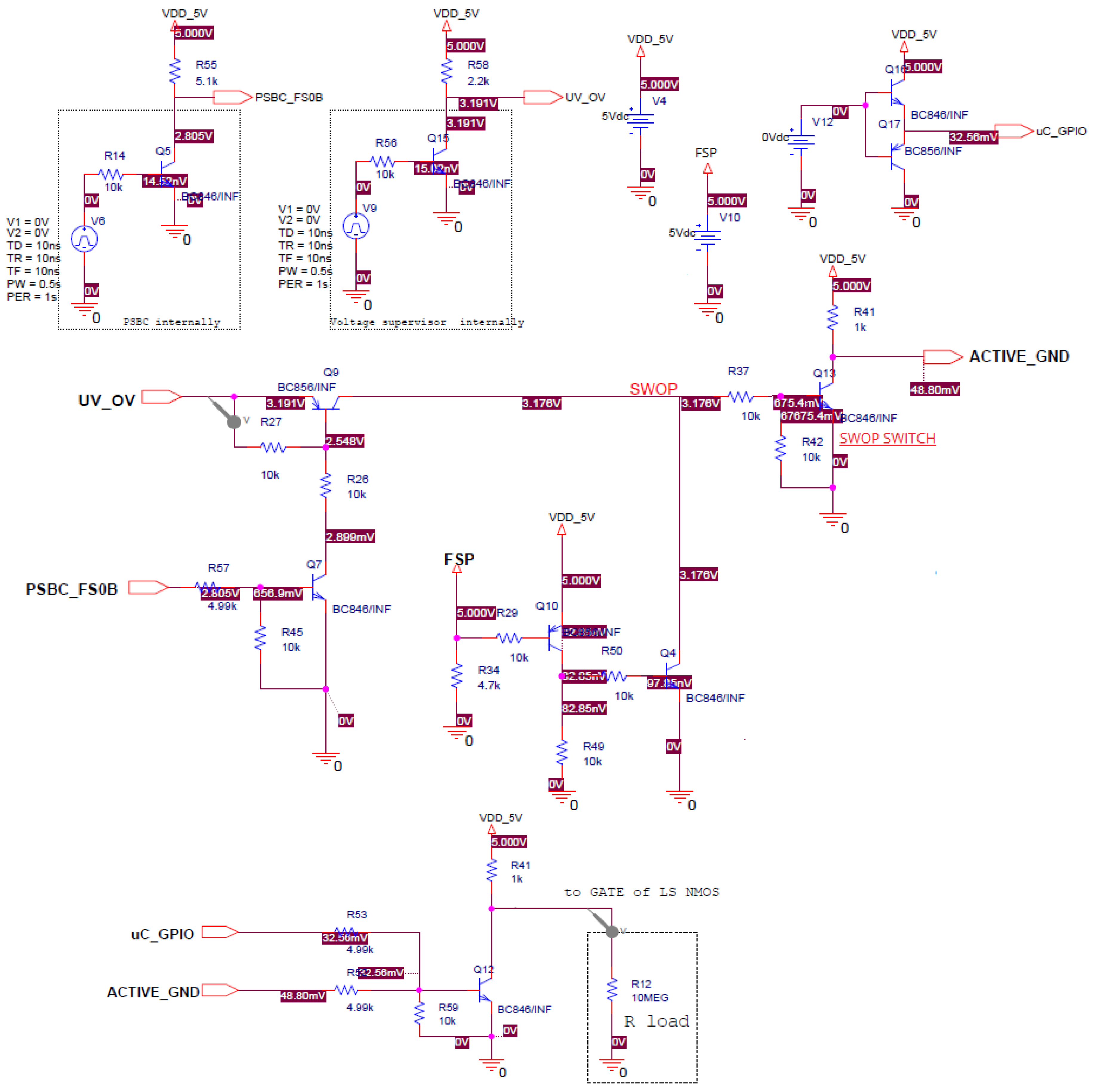
5.2. Safety Architecture for the Switch-Off Concept

Continuous monitoring of the voltage levels alone in critical applications may not be enough for safety implementation. Any out-of-order fault event detected by the redundant supervisors (the SBC via the internal FB_CORE, or the microcontroller via the PMS or voltage supervisory) needs to be reported in order to take appropriate corrective action (switch off or on the actuation, depending on the application). For TCUs, the SWOP represents the off position; all actuators will be stopped (e.g., motors will be put on break mode). For ACUs (airbag control units), this is also a safety-relevant application. The SWOP represents the on position for the switch-on path, because the appropriate restraint systems shall be triggered. When the SWOP is created, the designers shall consider in a redundant logic all the activation signals to guarantee the safe state of the application and cover the stringent ASIL-C or D requirements. A simple but efficient approach is the logic OR (a gate circuit which produces an output if there is a signal on any of its inputs). The article proposed a switch-off path architecture concept (represented by Figure 12) that is deployed by collecting in a node all the activation signals in a redundant way as follows:
  • FS0B from the SBC;
  • FSP from the microcontroller;
  • Redundant digital output pin from the microcontroller (GPIOR pin);
  • Under or overvoltage reset pin from the voltage supervisor block (OV/UV).
As listed in Step 6 of the design flow proposed in Section 2, before releasing the concept by the functional safety manager and stating the PCB manufacturing, it is mandatory to add proofs for proper functioning of safety activation using redundant logic. An OrCAD PSpice simulation of the circuit was performed, considering all four redundant signals (UV_OV, FS0B, FSP, uC_GPIO), as is depicted in Figure 13. For the FS0B and UV_OV signals from the voltage monitoring circuit, the internal open drain structure was emulated. Because the SWOP concept chosen is to switch off, an intermediary signal, called ACTIVE_GND, is considered. The function of this signal is as follows: only when ACTIVE_GND is low (0 V) and the uC_GPIO pin is low can the gate of the bridge switches (LS- low side MOSFETs) used in actuation be controlled. When a fault is raised by the FS0B, FSP, or UV_OU signals, ACTIVE_GND goes to a high level, which leads to the actuation switching off (gate pulled to the ground). After compiling the simulation for all cases and combinations of signals (low and high levels for each signal), the SWOP concept was released.
The schematic and layout board were started to finally obtain the evaluation board, a TCU board, as shown in Figure 14. On the PCB, voltage fault test cases were performed to see that the safety reaction was working as expected from the simulation. The measurements were performed with a digital multimeter by considering stable under or overvoltage faults (e.g., generating an external UV or OV fault) or open signals (e.g., disconnection pins). For all tested cases, the safe state was ensured and thus provided the reason for why the proposed SWOP concept could be extended to all safety-relevant applications.

6. Discussion

The focus of this paper was to provide a novel, safety-relevant supply design (with only 5 V delivered by an SBC to a microcontroller) which will withstand automotive requirements in terms of safety. The proposed design procedure was broken down into an original step-by-step action that every designer can follow to create a proper safety circuit between the supply and the microcontroller in safety-relevant applications. In other words, following the proposed design methodology, designers can reduce financial, legal, and safety risks and help to ensure satisfactory performance for an application in case of voltage faults. Hardware robustness was validated through worst-case analysis for proper selection of components. A complete safety reaction was considered and validated through simulation. In the SWOP circuit, there are four redundant ways to generate a safety reaction in case of over or undervoltage fault occurrence: three are software-based integrated solutions in the SBC and microcontroller and one is hardware-based on an external monitoring circuit. All four ways are essential for achieving safety, ensuring that the TCU design is robust and reliable upon voltage fault occurrence. Additionally, the authors plan to expand the method and supply concept for other ECUs with higher grades of ASIL requirements after a complete product validation.

Author Contributions

Writing—original draft preparation, D.R.B.; conceptualization, S.M.; methodology, S.M.; software, D.R.B. and A.I.; validation, D.R.B., A.I., and C.S.; formal analysis, D.R.B. and C.S.; investigation, D.R.B. and A.I.; resources, M.C.A.; data curation, C.S.; writing—review and editing, M.C.A.; visualization, S.M.; supervision, M.C.A.; project administration, M.C.A. All authors have read and agreed to the published version of the manuscript.

Funding

This research was funded by University POLITEHNICA Timisoara, GNaC2018 ARUT, no.1357/01.02.2019.

Acknowledgments

The authors would like to thank the Continental Automotive Powertrain Transmission Department for support, cooperation, and for disposal of equipment, tools, and resources, indispensable for the proposed investigation presented in this work.

Conflicts of Interest

The authors declare no conflict of interest.

References

  1. FS6500-FS4500—Safety Power System Basis Chip with CAN FD and LIN Transceivers—Datasheet (REV 6.0), 4 October 2017. Available online: https://www.nxp.com/docs/en/product-numbering-scheme/FS6500-FS4500SDS.pdf (accessed on 23 February 2019).
  2. ISO 26262—Road Vehicles—Function Safety; International Organization for Standardization. Available online: https://www.iso.org/standard/68383.html (accessed on 5 March 2019).
  3. IEC 61508 Standard—Electrical, Electronic and Programmable Electronic Safety Related Systems. Available online: https://www.iecee.org/dyn/www/f?p=106:49:0::::FSP_STD_ID:5516 (accessed on 26 February 2019).
  4. AURIXTM TC3xx. Available online: https://www.infineon.com/dgdl/Infineon-AURIX_TC3xx_Part1-UserManual-v01_00-EN.pdf?fileId=5546d462712ef9b701717d3605221d96 (accessed on 14 March 2019).
  5. Ismail, A.; Jung, W. Research trends in automotive functional safety. In Proceedings of the 2013 International Conference on Quality, Reliability, Risk, Maintenance, and Safety Engineering (QR2MSE), Chengu, China, 15–18 July 2013; pp. 1–4. [Google Scholar]
  6. Mariani, R. The impact of functional safety standards in the design and test of reliable and available integrated circuits. In Proceedings of the 2012 17th IEEE European Test Symposium (ETS), Annecy, France, 28–31 May 2012; p. 1. [Google Scholar]
  7. Park, J.S.; Suh, I.; Choe, C.Y.; Ro, M.; Brewerton, S.P. Intelligent ECU End of Line Testing to Support ISO26262 Functional Safety Requirements. SAE Int. J. Passeng. Cars Electron. Electr. Syst. 2013, 6, 162–168. [Google Scholar] [CrossRef]
  8. Leu, K.L.; Huang, H.; Chen, Y.Y.; Huang, L.R.; Ji, K.M. An intelligent brake-by-wire system design and analysis in accordance with ISO-26262 functional safety standard. In Proceedings of the International Conference on Connected Vehicles and Expo (ICCVE), Shenzhen, China, 19–23 October 2015; pp. 150–156. [Google Scholar]
  9. Hillenbrand, M.; Heinz, M.; Adler, N.; Matheis, J.; Müller-Glaser, K.D. Failure mode and effect analysis based on electric and electronic architectures of vehicles to support the safety lifecycle ISO/DIS 26262. In Proceedings of the 21st IEEE International Symposium on Rapid System Protyping, Fairfax, VA, USA, 8–11 June 2010; pp. 1–7. [Google Scholar]
  10. Chang, Y.C.; Huang, L.R.; Liu, H.C.; Yang, C.J.; Chiu, C.T. Assessing automotive functional safety microprocessor with ISO 26262 hardware requirements. In Proceedings of the 2014 International Symposium on VLSI Design, Automation and Test (VLSIDAT), Hsinchu, Taiwan, 28–30 April 2014; pp. 1–4. [Google Scholar]
  11. Azevedo, L.S.; Parker, D.; Walker, M.; Papadopoulos, Y.; Araújo, R.E. Assisted Assignment of Automotive Safety Requirements. IEEE Softw. 2014, 31, 62–68. [Google Scholar] [CrossRef]
  12. Takeichi, M.; Sato, Y.; Suyama, K.; Kawahara, T. Failure rate calculation with priority FTA method for functional safety of complex automotive subsystems. In Proceedings of the 2011 International Conference on Quality, Reliability, Risk, Maintenance, and Safety Engineering (ICQR2MSE), Xi’an, China, 17–19 June 2011; pp. 55–58. [Google Scholar]
  13. Sinha, P. Architectural design and reliability analysis of a fail operational brake-by-wire system from ISO 26262 perspectives. Reliab. Eng. Syst. Saf. 2011, 96, 1349–1359. [Google Scholar] [CrossRef]
  14. Siegl, S.; Hielscher, S.; German, K.R.; Berger, C. Formal specification and systematic model-driven testing of embedded automotive systems. In Proceedings of the Design, Automation & Test in Europe Conference & Exhibition (DATE), Grenoble, France, 14–18 March 2011; pp. 1–6. [Google Scholar]
  15. Grimm, T.; Djones Lettnin, I.D.; Hübner, M. A Survey on Formal Verification Techniques for Safety-Critical Systems-on-Chip. Electronics 2018, 7, 81. [Google Scholar] [CrossRef] [Green Version]
  16. Ferlini, F.; Seman, L.O.; Bezerra, E.A. Enabling ISO 26262 Compliance with Accelerated Diagnostic Coverage Assessment. Electronics 2020, 9, 732. [Google Scholar] [CrossRef]
Figure 1. Supply concept overview of a unique 5 V supply generated by a system basis chip (SBC).
Electronics 09 01580 g001
Figure 2. SBC (NXP) component nomenclature. Reproduced from [1].
Electronics 09 01580 g002
Figure 3. Microcontroller (AURIX Infineon) component nomenclature. Reproduced from [4].
Electronics 09 01580 g003
Figure 4. Proposed power supply design steps for safety-relevant applications.
Electronics 09 01580 g004
Figure 5. F6512 SBC 5 V, VCORE design. Reproduced from [1].
Electronics 09 01580 g005
Figure 6. Typical values recommended by the F6512 SBC datasheet.
Electronics 09 01580 g006
Figure 7. Buck converter stability in transient and Bode plots.
Electronics 09 01580 g007
Figure 8. Microcontroller proposed supply overview.
Electronics 09 01580 g008
Figure 9. Mathcad plot overview of the detection range in a worst-case scenario.
Electronics 09 01580 g009
Figure 10. F6512 SBC internal safety activation circuit. Reproduced from [1].
Electronics 09 01580 g010
Figure 11. TC397 Power management system block diagram. Reproduced from [4].
Electronics 09 01580 g011
Figure 12. Safety switch off path proposal for transmission control unit (TCU) safety activation.
Electronics 09 01580 g012
Figure 13. Simulation of safety switch-off path proposal for TCU safety activation.
Electronics 09 01580 g013
Figure 14. TCU evaluation board.
Electronics 09 01580 g014
Table 1. Microcontroller supply operation range.
TC3xx, C40 nm Technology
RangeBehavior
5.6–6.5 V60 h (Safety case, reset asserted, rated max. voltage +30%)
5.6–6.5 V10 h (Safety case, reset unasserted, rated max. voltage +30%)
5.3–5.6 V100 h (Safety case, reset unasserted)
4.5–5.3 V100% of lifetime (Normal functioning, rated max. voltage of 6%)

