Article

Multi-Chip IGBT Module Failure Monitoring Based on Module Transconductance with Temperature Calibration

School of Electrical Engineering and Automation, Wuhan University, Wuhan 430072, China
*
Author to whom correspondence should be addressed.
Electronics 2020, 9(10), 1559; https://doi.org/10.3390/electronics9101559
Submission received: 5 August 2020 / Revised: 20 September 2020 / Accepted: 21 September 2020 / Published: 23 September 2020
(This article belongs to the Special Issue Challenges and New Trends in Power Electronic Devices Reliability)

Abstract

:
The Insulated Gate Bipolar Transistor (IGBT) is the component with the highest failure rate in power converters, and its reliability is a critical issue in power electronics. IGBT module failure is largely caused by solder layer fatigue or bond wires fall-off. This paper proposes a multi-chip IGBT module failure monitoring method based on the module transconductance, which can accurately monitor IGBT module chip failures and bond wire failures. The paper first introduces the failure mechanism and module structure of the multi-chip IGBT module; then, it proposes a reliability model based on the module transconductance and analyzes the relationship between chip failure, bond wire failure, and the transmission characteristic curve of the IGBT module. Finally, the module transconductance under chip failure and bond wire failure is measured and calculated through simulation, and the temperature is calibrated, which can eliminate the influence of temperature on health monitoring. The results show that the method has a high sensitivity to chip failures and bond wire failures, can realize the failure monitoring of multi-chip IGBT modules, and is of great significance for improving the reliability of power converters.

1. Introduction

The Insulated Gate Bipolar Transistor (IGBT) module is a power electronic integrated module composed of multiple IGBT chips, diode chips, solder layers, bond wires, ceramic copper-clad substrates, heat dissipation base plates, and power terminals. IGBT modules are mainly used in inverters, frequency converters, uninterruptible power supplies, wind power, and solar power generation. They are the core components of power converters and have one of highest failure rates out of all the power converters [1]. To reduce the failure rate and improve the reliability of the power converter, it is of great significance to monitor the failure status of the IGBT module [2].
At present, many scholars at home and abroad are committed to the reliability research of IGBT modules, most of which focus on the online measurement of IGBT health-sensitive parameters (HSPs) or thermosensitive electrical parameters (TSEPs). Researchers measure the collector, gate, emitter, and appropriate Kelvin terminals of the IGBT module to obtain the external electrical parameters of the IGBT module, and realize the health monitoring of the IGBT module through the fault characteristic parameters [3,4,5]. Reference [6,7] proposed measuring IGBT saturation voltage drop VCE(sat) during the operation of the power converter. This method must ensure that the measured current is constant during operation, but it is difficult to achieve in practice. Reference [8,9,10] proposes using the on-state voltage drop VCE(ON)a under load current to monitor the shedding of IGBT bond wires in real time. Still, this parameter has a weak anti-interference ability. In reference [11], the on-state voltage drop VCE(on)B at the inflection point is used to monitor the aging and shedding of bond wires, which has strong resistance to junction temperature interference. However, the measurement of the on-state voltage drop VCE(ON) needs to consider the high-voltage isolation problem, and the measurement is from thousands of volts in the off phase to a few volts in the on phase. The measurement range is broad, and the measurement circuit must consider a large VCE voltage swing. There are certain difficulties in practical applications. Reference [12] uses on-state resistance RCE(ON) to monitor the aging degree of the IGBT module package online. Although it has high sensitivity, its resistance to junction temperature interference is low, and the first bond wire lift-off in the IGBT module cannot be detected. Reference [13,14,15] uses the peak gate current IGPeak to monitor the shedding of the bond wire in the parallel IGBT module. Although this parameter has a strong resistance to changes in junction temperature, detecting the peak gate current value is difficult in practical applications. In addition, the gate current is relatively small, and the measurement is performed on the side close to the IGBT module. The detection circuit also needs to deal with the challenge of electromagnetic interference. In reference [16], the grid emitter voltage variation dVCE/dt was used to detect the drop of the bond wire during the process of turning the circuit on and off. This method could not identify the first bond wire lift-off. Reference [17] proposes using the gate-emitter pre-threshold voltage VGE(pre-th) to monitor IGBT chip failures in multi-chip IGBT modules. This method can only monitor chip failures and cannot monitor a small number of bond wire fall-off failures. Most of the above research methods can only monitor one of the failures of the IGBT bond wire lift-off or the IGBT chip failure, and it cannot be monitored at the same time. Temperature-sensitive electrical parameters need to be considered when used as fault characteristic parameters. However, in the above studies, temperature-sensitive electrical parameters have not been normalized to eliminate the impact of temperature on failure monitoring.
Aiming at the shortcomings of the existing research methods, this paper proposes using the IGBT module transconductance as the characteristic quantity to identify both the chip failure and the bond wire failure in the multi-chip IGBT module and realize the failure monitoring of the IGBT module. The paper first analyzes the failure mechanism and module structure of the multi-chip IGBT module; then, it proposes a reliability model based on the module transconductance and analyzes the relationship between chip failure, bond wire failure, and the IGBT module transmission characteristic curve (iC-uGE) Finally, the quantitative relationship between chip failure and bond wire failure and module transconductance is measured and calculated through simulation. Furthermore, the temperature is normalized, which can eliminate the influence of temperature on failure monitoring. The results show that the method has good sensitivity to chip failures and bond wire failures, can realize the failure monitoring of multi-chip IGBT modules, and is of great significance for improving the reliability of power converters.
The sections of this article are arranged as follows. In Section 2, the failure mechanism and module structure of the multi-chip IGBT module are introduced in detail. In Section 3, a reliability model based on the module transconductance is constructed. Section 4 is based on the reliability model to monitor the chip failure and bond wire failure status of the DIM800NSM33-F IGBT module. The results are discussed and analyzed in Section 5.

2. Multi-Chip IGBT Module Failure Mechanism and Structure

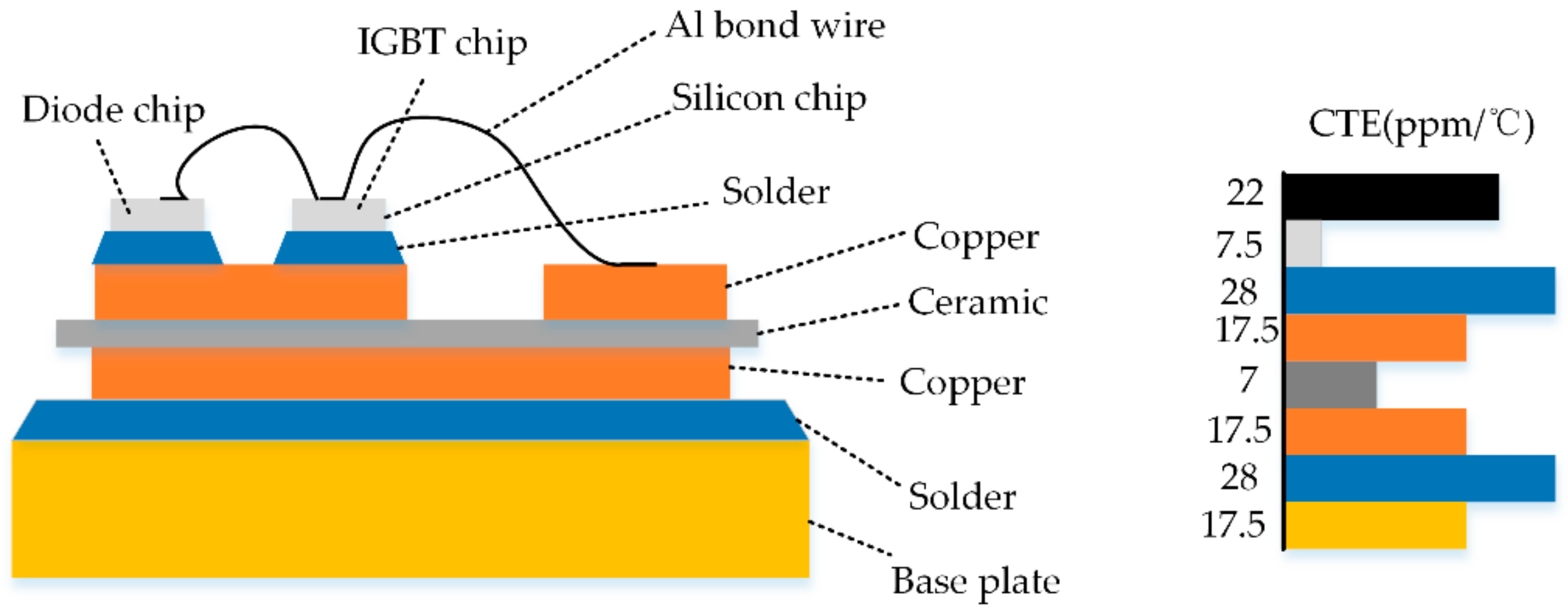
The failure of the solder layer and the falling off of the bond wires are the main aging failure mechanisms of IGBT modules. The bond wire is mainly used to connect the chip (IGBT chip or diode chip) and the terminal (gate or emitter). The main reason for the bond wire to fall off is the inconsistent coefficient of thermal expansion (CTE) of each layer of the semiconductor device. Figure 1 shows the IGBT module packaging structure and the coefficient of thermal expansion of each layer of material. The IGBT chip and the diode chip are electrically connected by bond wires, as are the chip and the copper substrate. During the normal operation of the IGBT, the heat generated by the power loss of the semiconductor chip will pass through the multi-layer structure to the heat sink to produce a junction temperature fluctuation ΔT, which causes the bond wire to generate shear stress at its welding point, and the changing stress produces cracks, which leads to the bond wires fall-off [18,19]. Initially, cracks are generated at both ends of the bond wire; then, they are gradually extended to the middle until the bond wire completely falls off. Once a bond wire in the module falls off, the current passing through the remaining bond wires will increase immediately, thereby accelerating the fall-off process of the remaining bond wires [20]. The deformation εt of the IGBT due to the fluctuation of the junction temperature can be expressed by Equation (1):
εt = LAl − αSi)·ΔT
where αAl and αSi are the CTEs of aluminum and silicon, L is the length of the aluminum bond wire; ΔT is the junction temperature fluctuation.
For multi-chip IGBT modules, in addition to the parasitic parameters of the cell chip, stray parameters such as the substrate, board lining, solder layer, and bond wire in the module packaging process need to be considered [21]. Among the stray parameter changes caused by IGBT failure, the bond wire fall-off is the most typical. Therefore, the chip fault and bond wire fault studied in this paper are caused by the bond wire fall-off. If the bond wires of a certain unit IGBT chip are all falling off, the number of effective IGBT chips connected in parallel in the IGBT module will be reduced, and the fault type is chip failure at this time. If the bond wire of a certain unit IGBT chip falls off, the number of effective bond wires on the chip will be reduced, and the fault type is bond wire failure at this time. The reliability of multi-chip IGBT modules depends on the health of all parallel IGBT chips and bond wires. Therefore, it is very important to evaluate the overall health of the multi-chip IGBT module by monitoring IGBT chip failure and bond wire failure [22].
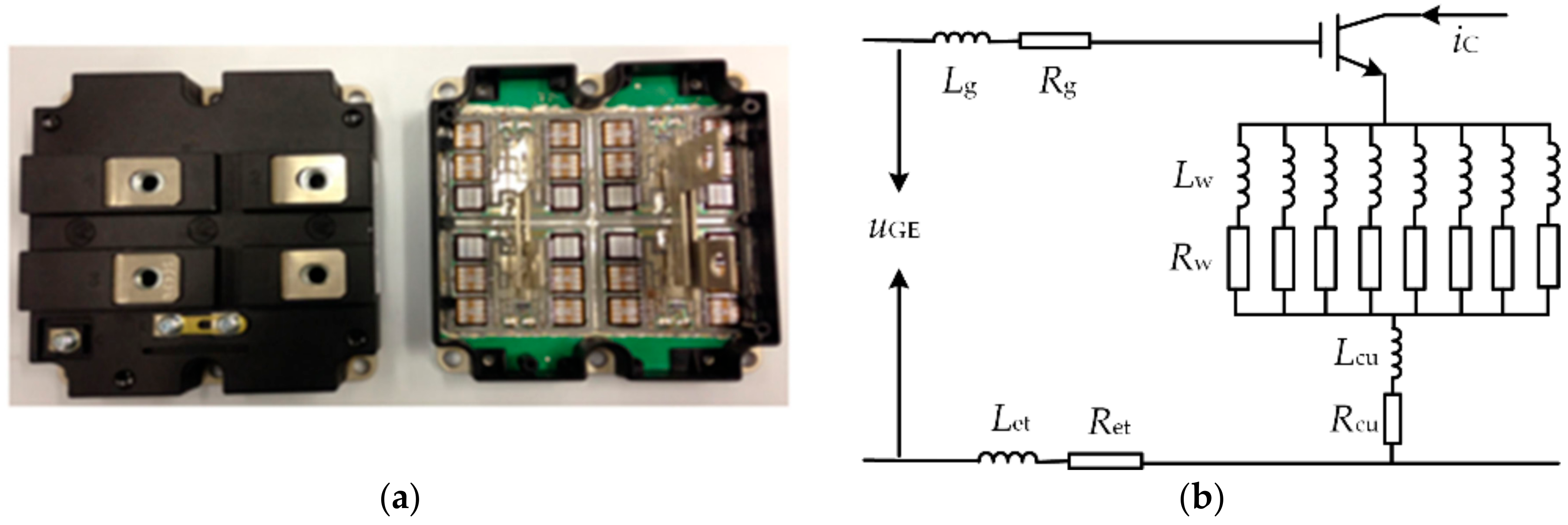
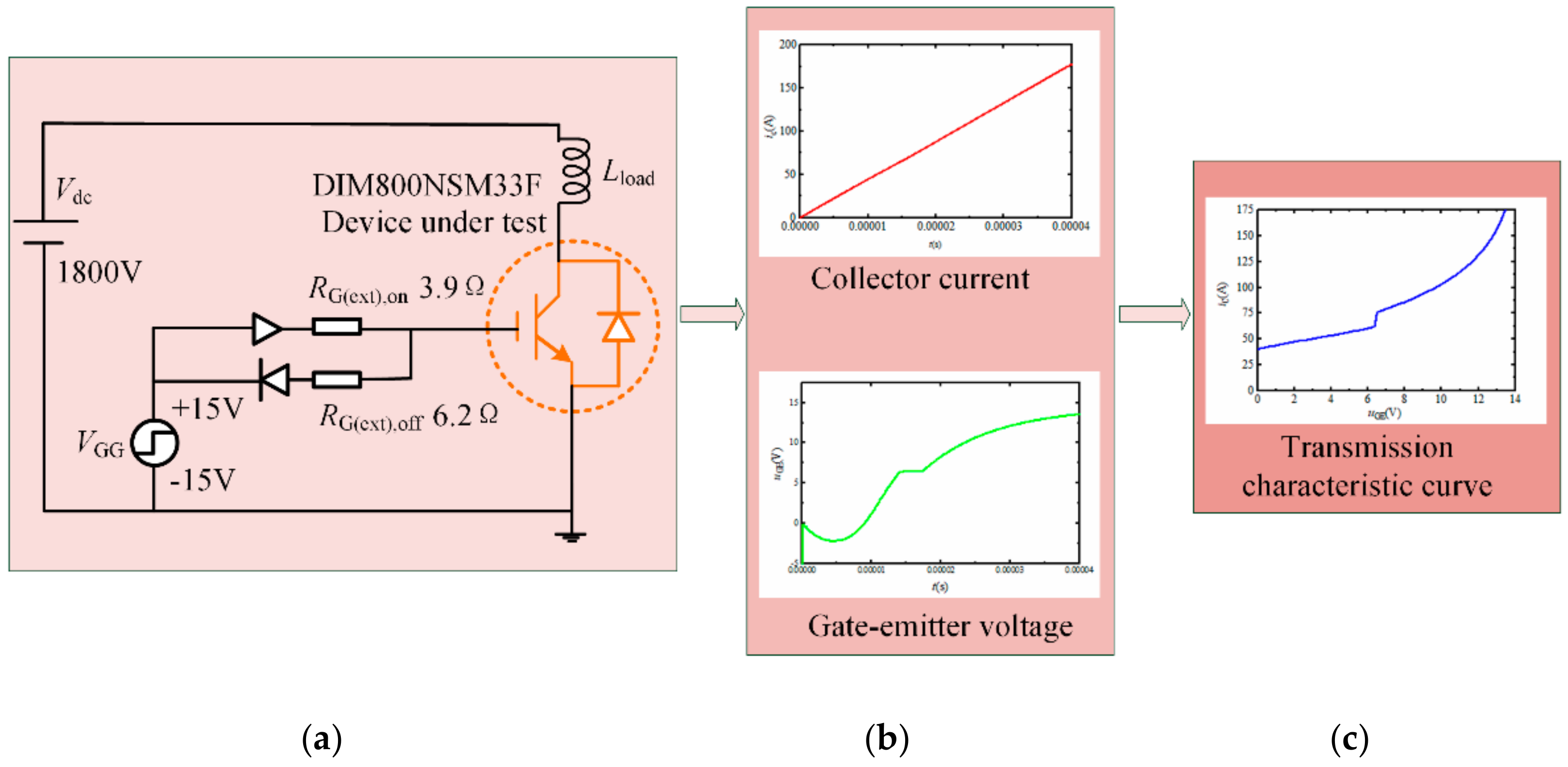
Figure 2 shows the equivalent diagram of the internal structure of the multi-chip IGBT module. There are n IGBT chips in parallel. This article takes the DIM800NSM33-F IGBT module as the research object. This module is a commercial module. The physical map and the internal equivalent circuit of a single chip in the module are shown in Figure 3. The module is a 16-unit IGBT module. Each chip has eight emitter bond wires, and there are 128 emitter bond wires in total. Refer to the data sheet for the basic parameters of the module, as shown in Table 1. The acceptable number of chip losses for IGBT modules depends on the working environment and working requirements. Generally, 10% chip losses in IGBT modules and 70% bond wire lift-off on the chip are considered acceptable [23]. Therefore, for the DIM800NSM33-F IGBT module, the detection of two chip failures in 16 chips is set as the safety margin. The failure simulation is the situation of the first two chips that failed; the first chip that failed is called “Chip 1”, the second chip that failed is called “Chip 2”.

3. Reliability Model Based on Module Transconductance

The transmission characteristic curve of the IGBT module usually adopts Auto Curve Tracer to test, the horizontal axis is the gate-emitter voltage uGE, and the vertical axis is the collector current iC, which is affected by temperature. The general definition of transconductance refers to the slope of the transmission characteristic curve of the IGBT chip, which is the characteristic parameter of the IGBT chip itself. For the entire IGBT module, its module transconductance is affected by IGBT chip fatigue and bond wire failure. The transmission characteristic of IGBT refers to the response function of iC to uGE changes at different temperatures. The gradient of the transmission characteristic at a given temperature is called the transconductance of the device at that temperature. IGBT is a device that uses input voltage to control output current. The ratio of output current to input voltage is represented by transconductance, which also reflects the gain of IGBT. The chip transconductance gmc reflects the sensitivity of ic to uGE, and the module transconductance gm reflects the sensitivity of ic to ui. This article mainly focuses on the failure research of the IGBT module chip and bond wire, which belongs to module package level failure: a slow and gradual process.
The relationship between IGBT chip fatigue, bond wire lift-off, and module transconductance is analyzed in detail below. According to the working principle of the IGBT chip, when the IGBT chip operates in the active area, the governing equation of the collector current ic is shown in Equation (2) [24]:
i c = μ ni C OX Z 2 L ( 1 α pnp ) ( u G U GE ( th ) ) 2 = A ( u GE U GE ( th ) ) 2
where μni is the electron migration speed, COX is the oxide layer capacitance, Z and L are the length and width between the gate-emitter of the MOSFET, αpnp is the current gain of the PNP transistor, UGE(th) is the threshold voltage of the IGBT chip; the above parameters are all determined by the chip structure and material, but they are all affected by the junction temperature Tj of the chip.
For simplification, the parameter A is used to characterize the parameters related to the physical size and structure of the chip in Equation (2), and the chip transconductance gmc is the sensitivity of ic to uGE as shown in Equation (3):
g mc = d i c d u GE = 2 A ( u GE U GE ( th ) ) .
From Figure 3b, we can see that for a single IGBT branch, the circuit equation during the switching transient device is Equation (4):
u G = u i i C R w L G d i G d t i G R G ( L cu + L et ) d ( i G + i C ) d t ( i G + i C ) ( R cu + R et )
where Rw is the equivalent parasitic resistance of bond wires; Rcu and Lcu are the equivalent parasitic resistance and inductance of the copper layer; ui is the gate drive voltage of the IGBT module; and iG is the gate current of the IGBT module. Let is the equivalent stray inductance of the IGBT emitter lead, and Ret is the equivalent stray resistance of the IGBT emitter lead.
The parasitic resistance of the IGBT is about 40 μΩ, the parasitic inductance is about 30 nH, and the bonding wire resistance is about 50 mΩ. The parasitic resistance and all parasitic inductances are relatively small compared to the bonding wire resistance. In practical applications, dic/dt is about 3000 A/μs, and dig/dt is about 0.2 A/μs. When the IGBT works in the safe active region, the collector current ic and the gate current ig remain almost constant. Considering that the measurement of the transconductance gm of the detection parameter module in this paper is when the IGBT is working in the safe active area, Equation (4) can be simplified to Equation (5):
uG = uiicRw.
When ui is equal to UGE(th), the current flowing through the IGBT is zero. In order to study the influence of IGBT module transconductance and bond wire resistance RW on the module transconductance, we substitute Equation (5) into Equation (1) and perform appropriate transformations to obtain the relationship between ic and ui as Equation (6):
i c = 2 A R w u i U GE ( th ) + 1 4 A R w u i U GE ( th ) + 1 2 A R w 2 .
The module transconductance gm of the IGBT module reflects the sensitivity of ic to ui, which can be derived as Equation (7):
g m = d i c d u i = 1 R w 1 1 4 A R w u i U GE ( th ) + 1 .
Comparing Equations (2) and (6), we can see that the relationship between chip transconductance gmc and module transconductance gm is as shown in Equation (8):
g m = 1 R w + 1 / g mc .
The transconductance of the IGBT module is not only related to the transconductance of the IGBT chip itself but also to the health of the parallel chip and the bond wires. The module transconductance will decrease as Rw increases during the aging failure process. From Equation (2), we can get Equation (9):
u i U GE ( th ) = R i c A + i c A .
Then, we put Equation (9) into Equation (7) to get the module transconductance, as shown in Equation (10). The transconductance expression of this module has nothing to do with the threshold voltage affected by the gate oxide layer.
g m = 1 R w 1 1 4 A i c R w 2 + 4 A i c R w + 1
Among the failure modes of power devices, package-related failures are the most common and are generally considered to be the main factors affecting the life of IGBTs. It can be seen from Equation (10) that the module transconductance is a function of parameter Rw, parameter A, and collector current ic. Parameter A characterizes the physical size and structural parameters of the chip, and it is generally believed that these parameters will not change with aging. In this case, the bond wire lift-off is the only aging factor that affects the module transconductance change. For multi-chip IGBT modules, the chip characteristics and bond wire resistance on each branch may not be consistent, and the gate oxide degradation of each chip may also be different. For simplicity, it is assumed that the chip branches are consistent, and the aging process is also consistent, so as to eliminate the influence of the threshold voltage UGE(th).
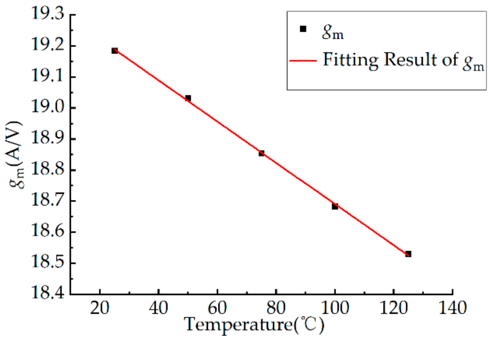
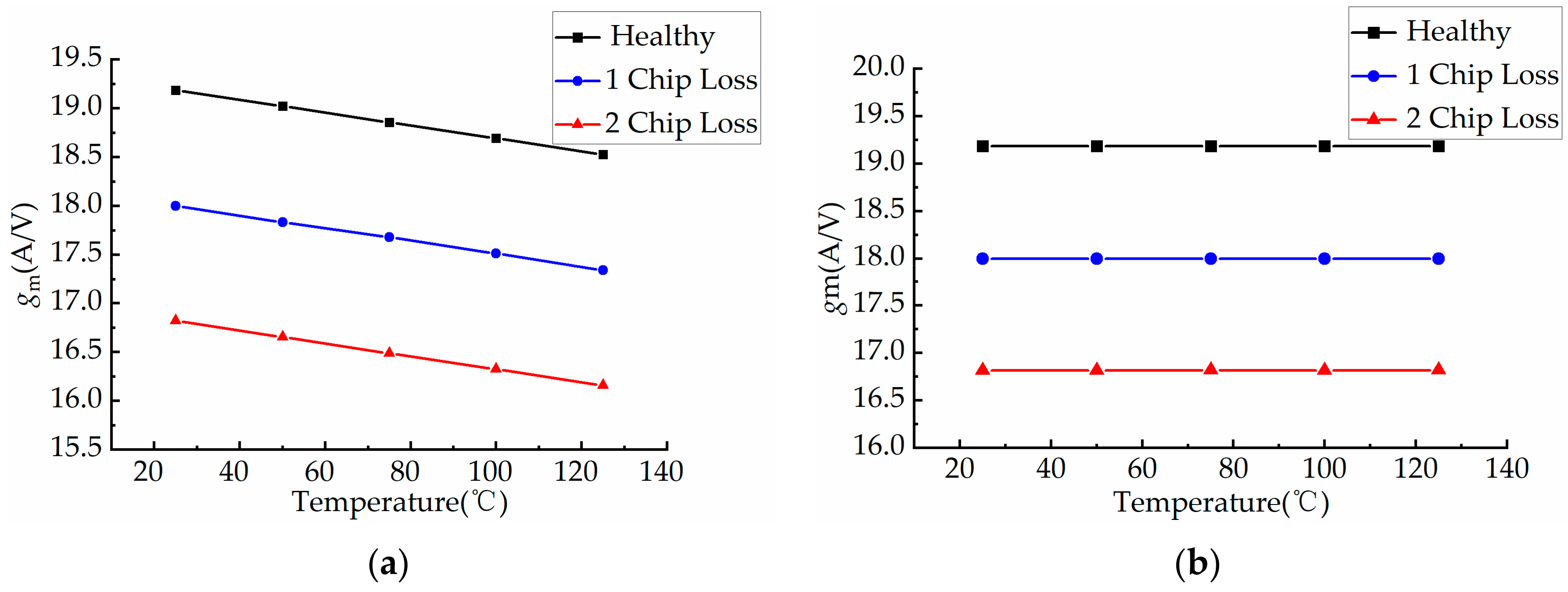
The junction temperature will affect the electrical characteristics of the IGBT. The dependence of the physical material parameters of the silicon-based semiconductor on temperature determines the temperature dependence of its operating characteristics. The lifetime of carriers increases with the decrease of temperature and mobility, and the charge storage in the drift region decreases with the increase of temperature, so the IGBT switching process is affected by temperature. In the IGBT module, both the parameter Rw and the parameter A are affected by the junction temperature, and the transconductance of the module under the same collector current can be expressed as Equation (11):
gm = f(Rw,T).
In actual engineering, with the aging of the IGBT module, the equivalent resistance of the module will change accordingly. At the same time, the junction temperature Tj will also fluctuate during the normal operation of the power converter [25,26]. The influence of fluctuation on the transconductance of the module can be expressed by Equation (12):
Δ g mi _ T = f T i , R w 0 f T 0 , R w 0 Δ g mi _ Rw = f T 0 , R w i f T 0 , R w 0
where T0 is the selected reference temperature; Rw0 is the equivalent resistance of bonding wire in the healthy state of the IGBT module; Ti is the temperature after change; and Rwi is the bond wire equivalent resistance after module aging failure.
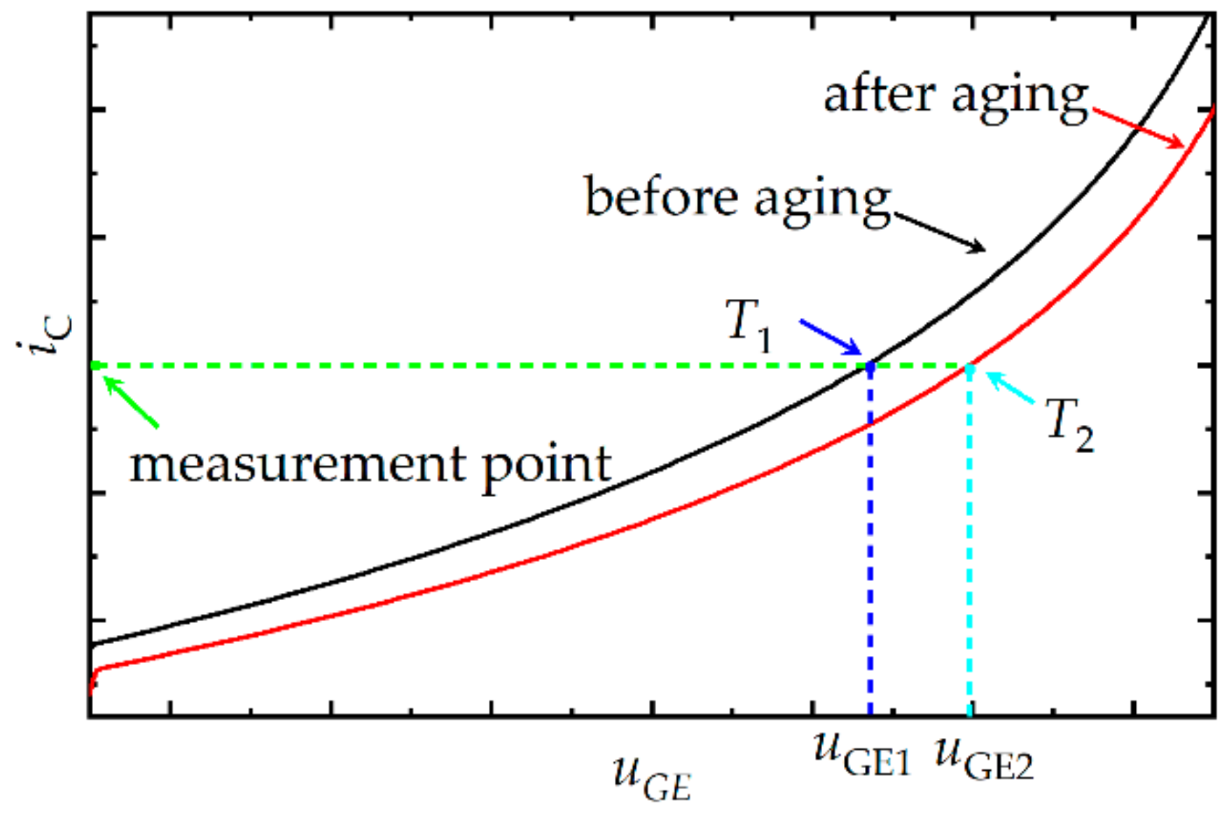
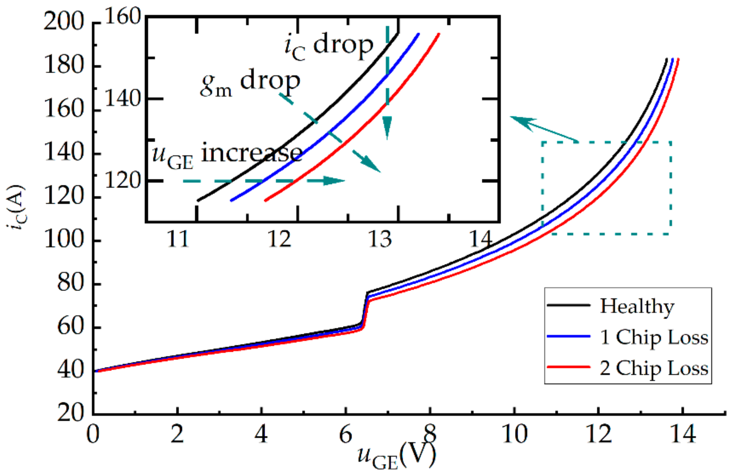
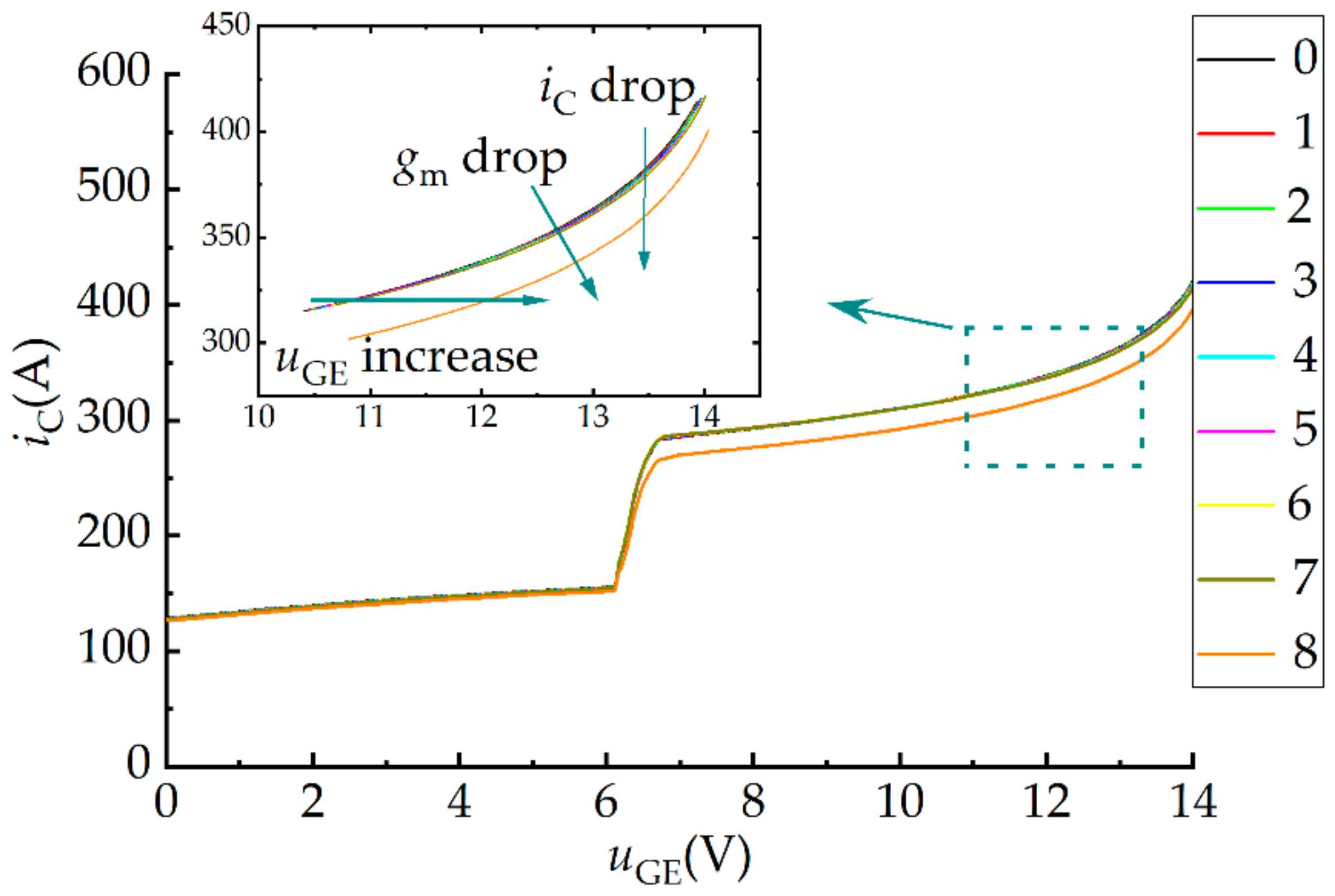
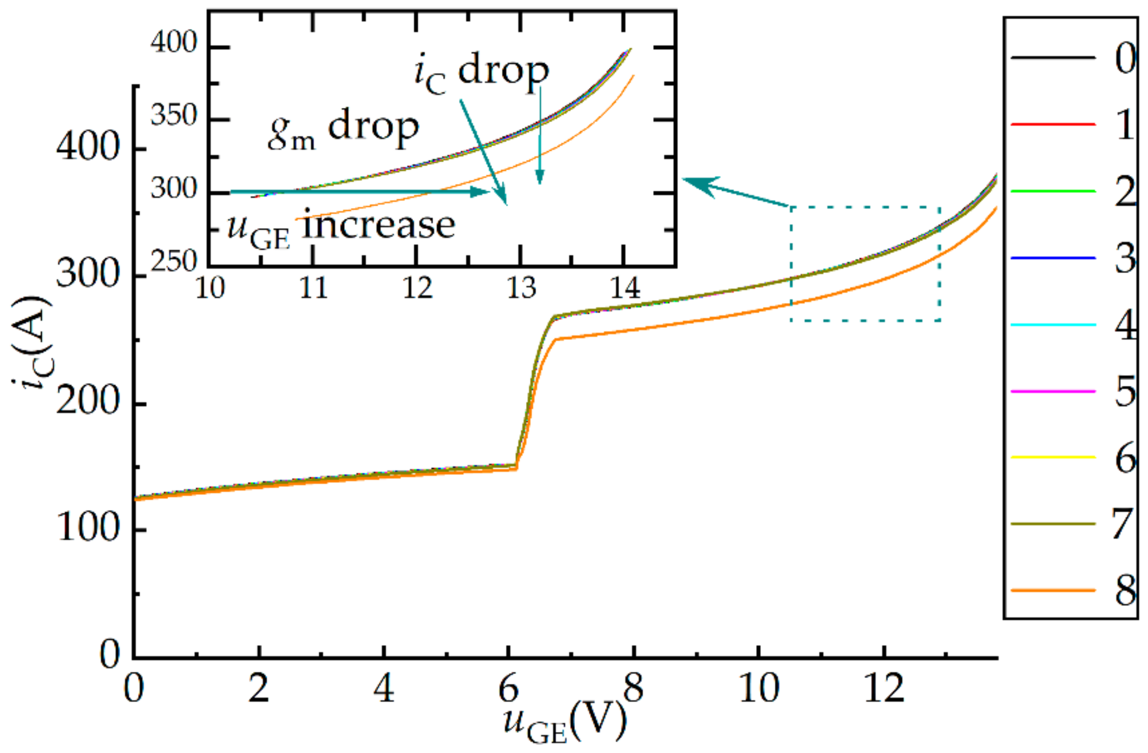
Figure 4 shows the transmission characteristic curve before and after the IGBT module bonding wire lift-off. As the bond wires fall off, the collector current gradually decreases in the active area. At the same collector current iC measurement point, the gate-emitter voltage after the bond wire falling off increases from uGE1 to uGE2, and the power loss of the IGBT module will also increase, which will lead to an increase in junction temperature and failure of the bond wire. The resulting junction temperature difference is T2T1. Therefore, when the module transconductance is used to monitor the health of a multi-chip parallel IGBT module, it is necessary to eliminate the effect of junction temperature. The extraction of module transconductance requires the chip to work in the active area, and it is also necessary to consider that the IGBT module is located in the safe operating area (SOA).

4. Model and Test

Figure 5 shows the schematic diagram of multi-chip IGBT module failure monitoring based on module transconductance. According to the test circuit, the collector current and gate emitter voltage are measured to obtain the transmission characteristic curve, and then the transconductance of the module is calculated according to the transmission characteristic curve. The DC bus power supply voltage of the test circuit is 1800 V, and the load is an inductive load of 400 μH. The tested IGBT module is driven by the gate driver with a voltage pulse of approximately −15 to +15 V. Between the ideal pulse voltage power supply and the IGBT gate terminal, 3.9 Ω turn-on gate resistance RG(ext),on and 6.2 Ω turn-off gate resistance RG(ext),off are used. In this paper, the test of the transmission characteristic curve under the condition of chip failure and bonding wire failure is completed in Matlab/Simulink.

4.1. IGBT Chip Failure

The type of chip failure studied in this paper is that all bond wires on a chip fall off or the IGBT chip is completely fatigued due to the optimus effect caused by overcurrent, overvoltage, overheating, or beyond the shutdown safe working area. The research object DIM800NSM33-F IGBT module of this paper is a multi-chip parallel IGBT module. All parallel chip branches are regarded as the same, and chip failure is simulated by changing the number of parallel chip branches. Considering the safety margin of the module under study—two chip failures, the chip position has a relatively small influence, so the influence of the chip failure position is not considered for the time being. Select the reference temperature T0 = 2 °C, and consider the safety margin of the selected IGBT module. In the above model, the IGBT module is tested under three different health conditions: “health”, “one chip failure”, and “two chip failure”. The transmission characteristic curve of the IGBT module under different chip fault conditions is shown in Figure 6. With the increase of the number of chip failures, under the same collector current iC, the gate-emitter voltage uGE gradually increases; under the same gate-emitter voltage uGE, the collector current iC gradually decreases. The slope of the transmission characteristic curve of the IGBT module also decreases gradually. That is, the transconductance of the IGBT module decreases gradually. When the gate voltage uGE is less than the threshold voltage VGE(th), the IGBT is in the off state. In most of the collector current range after the IGBT is turned on, iC and uGE have a good positive correlation. Considering that the IGBT works in the active area and is located in the safe working area, and the transmission characteristic curves have obvious differences under different fault conditions, the uGE value is selected as 12 V to calculate the transconductance value of the module. According to the transmission characteristic curve, the transconductance value of the IGBT module under different chip fault states is calculated, as shown in Table 2. It can be seen that the transconductance of the module gradually decreases with the increase of IGBT failure chips, and the transconductance of the module decreases by about 6.2% when an IGBT chip fails. When two IGBT chips in the module fail, the transconductance of the module is reduced by 12.472%. At this time, the health status of the module has exceeded the safety margin, and the module is close to failure. It should be repaired or replaced in time to improve the reliability of the power converter.
When the IGBT is aging and failing, it will cause changes in parameters such as the thermal resistance and heat capacity, which will change the junction temperature of the IGBT, which will affect the transconductance parameters of the IGBT module. This article attributes the effect of aging failure to the effect of temperature on the transconductance, so it is necessary to exclude the effect of temperature on the module transconductance. When the IGBT module was in a healthy state, that is, when there was no chip failure and no bond wire fall-off, we measured and calculated the transconductance of the IGBT module at 25, 50, 75, 100, and 125 °C, as shown in Table 3. When the module is in a healthy state, as the temperature increases, the transconductance of the IGBT module gradually decreases. Figure 7 shows the relationship between the IGBT module transconductance and temperature. It can be seen from the figure that the module transconductance and temperature show a very good linear relationship, so the linear fitting can be used to obtain the module transconductance and temperature. The relationship, as shown in Equation (13), has a linear fit of up to 0.998. In order to eliminate the influence of temperature, the module transconductance at different temperatures can be calibrated to 25 °C according to Equation (13). At this time, the module transconductance is only related to the module’s health status.
gmT,j_25 °C = gmT,j + 0.00664 (T − 25)
where T is the temperature, j is the module’s different health states, gmT,j is the transconductance at different temperatures and different health states, and gmT,j_25 °C is the module’s transconductance calibrated to 25 °C.
We tested different IGBT chip fault types at 25, 50, 75, 100, and 125 °C and calculated the IGBT module transconductance, as shown in Table 4. It can be seen that the module transconductance decreases as the number of IGBT chips increases, and it decreases as the temperature increases. Figure 8a shows the module transconductance under different temperatures and health conditions. Within a certain temperature range, the module transconductance can be used to determine the number of IGBT module chip failures and realize the health status monitoring of the IGBT module.
In order to monitor the health status of the IGBT module more accurately and eliminate the influence of temperature, the module transconductance at different temperatures is calibrated to the reference temperature T = 25 °C according to Equation (13). Figure 8b shows the module transconductance after temperature calibration. Compared with the module transconductance that has not undergone temperature correction, gm after temperature calibration is only related to the module’s health status. The latter can more intuitively and clearly judge the type of chip failure and more accurately assess the health of the IGBT module status.

4.2. Bond Wire Failure

The bond wire failure studied in this paper is caused by the bond wire lift-off. The DIM800NSM33-F IGBT module has eight bond wires on each IGBT chip. Considering the maximum safety margin of the IGBT module, the following will test and analyze different types of bond wire faults on Chip 1 and Chip 2.
For Chip 1, the state of the bond wire is i (i = 0, 1, 2, …, 8) bond wire lift-off. When the reference temperature TC = 25 °C, the transmission characteristic curve of the measurement of Chip 1 under different bond wire failure states is shown in Figure 9. After the eighth bond wire lift-off, the transmission characteristic curve is completely separated from other curves, and Chip 1 is completely invalid at this time. This is because all the bond wires fall off so that the chip is completely faulty and invalid, and the electrical characteristics of the IGBT module have changed significantly, making the transmission characteristic curve clearly separated. According to the transmission characteristic curve, the module transconductance corresponding to the number of bond wire shedding is calculated, as shown in Table 5. It can be seen from Table 5 that the module transconductance gradually decreases with the increase in the number of bond wires falling off. Each time a bond wire lifts off, the module transconductance decreases about 0.753% on average. When the last bond wire falls off, the transconductance of the module changes significantly.
The same measurements and calculations are done for different bond wire fault states of Chip 1 at different temperatures, and the module transconductance is obtained, as shown in Table 6. It can be seen from Figure 10a that under the same bond wire state, the temperature is different, the module transconductance value is also different, and the temperature has a great influence on the type of bond wire failure of the monitoring of Chip 1, and it is impossible to accurately determine the number of Chip 1 bond wires falling off. For example, when Chip 1 is in a healthy state, the decrease of the module transconductance caused by the temperature increase may be misjudged as a bond wire failure state.
In order to reduce the error rate of bond wire fault monitoring and improve the accuracy of IGBT module health monitoring, it is necessary to eliminate the influence of temperature. Therefore, Equation (13) can be used to calibrate the module transconductance at different temperatures to the reference temperature TC = 25 °C, as shown in Table 7; then, the temperature calibrated module transconductance can be used to achieve IGBT module health condition monitoring. The module transconductance interval is different under different bond wire failure states; that is, the module transconductance difference is different, and the percentage of change is different. When the last bond wire falls off, the module transconductance interval is the largest, and the module transconductance change is the largest. The module transconductance and junction temperature show a good linear relationship under the bonding wire failure state. Figure 10b shows the transconductance of the IGBT module after temperature correction. It can be seen from the figure that the calibrated module transconductance can accurately distinguish the chip bonding wire off at any temperature, and it is basically not affected by temperature changes. It can accurately monitor the health status of the IGBT module.
Similarly, in order to monitor the health status of the bond wires of Chip 2, when the temperature is 25 °C, the transmission characteristic curves of different bond wires of Chip 2 under fault conditions are measured, as shown in Figure 11. The change rule of the transmission characteristic curve is the same. According to the calculation of the transmission characteristic curve, the module transconductance corresponding to the number of bond wires lift-off is shown in Table 8. It can be seen from Table 8 that the module transconductance gradually decreases with the increase in the number of bond wires lift-off. For each bond wire lift-off, the module transconductance decreases by about 0.812% on average. The change rule is basically the same as that of the Chip 1 bond wire failure state.
In order to study the influence of temperature on the monitoring of the fault state of the bond wire of Chip 2, the transmission characteristic curves of different bond wire fault states are measured at temperatures of 25, 50, 75, 100, and 125 °C, and the IGBT is obtained by calculation. The module transconductance is shown in Table 9. It can be seen from Figure 12a that with the increase of temperature, the module transconductance decreases gradually, which is consistent with the change of the number of bond wires lift-off. The increase of IGBT module transconductance caused by temperature rise is easy to be misjudged as the falling off of bond wire, so the influence of temperature change will interfere with the monitoring of the failure state of bond wires.
In order to eliminate the interference of temperature factors on health status monitoring, Equation (13) is used to normalize the module transconductance at different temperatures to the reference temperature Tc = 25 °C, as shown in Table 10. Then, the module transconductance after temperature calibration is used to monitor the health status of the IGBT module. Figure 12b shows the transconductance of the IGBT module after temperature correction. It can be seen from the figure that the calibrated module transconductance can accurately distinguish the chip bond wire lift-off condition at any temperature and monitor the health status of the IGBT module.

4.3. Result Verification

In the reference [27] “Research on Accelerated Aging and Aging Characteristic Parameters of IGBT Modules”, the author chooses multi-chip parallel IGBT modules as the research object and uses the method of artificial wire cutting to simulate the falling off of the IGBT module bonding wires. Among them, the experimental test results of Chip 1 falling off zero, one, two, three, and four bonding wires are shown in Table 11. The simulation results of this article are also recorded in Table 11 for comparison.
It can be seen from Table 11 that the transconductance gm of the two modules are similar, and with the increase in the number of bond wires falling off, the change trend and rate of change of the transconductance gm of the module are also very close; that is, the parallel IGBT module experiment result is similar to the parallel IGBT module simulation. The results are basically the same, with only slight differences, and the number of bond wires falling off can be judged by the percentage of transconductance change. Therefore, based on the experimental data, this paper can preliminarily show that the theoretical method and simulation results are correct and effective.

5. Result Analysis

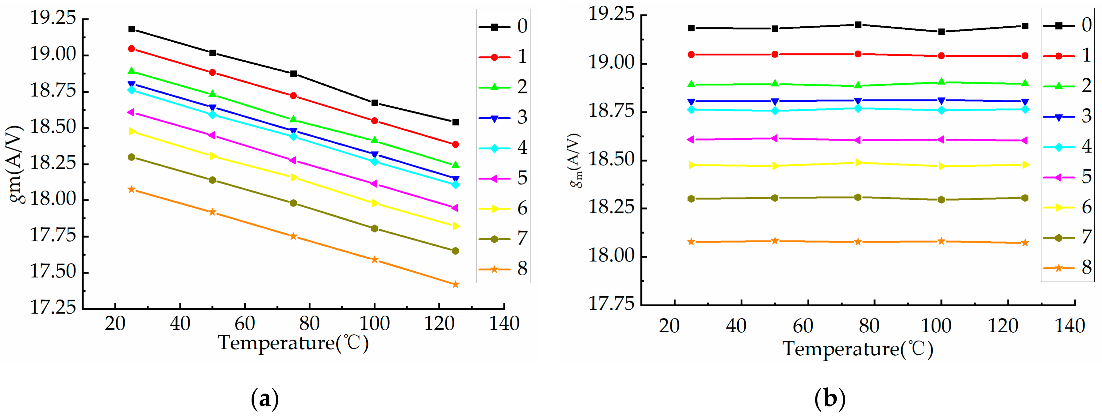
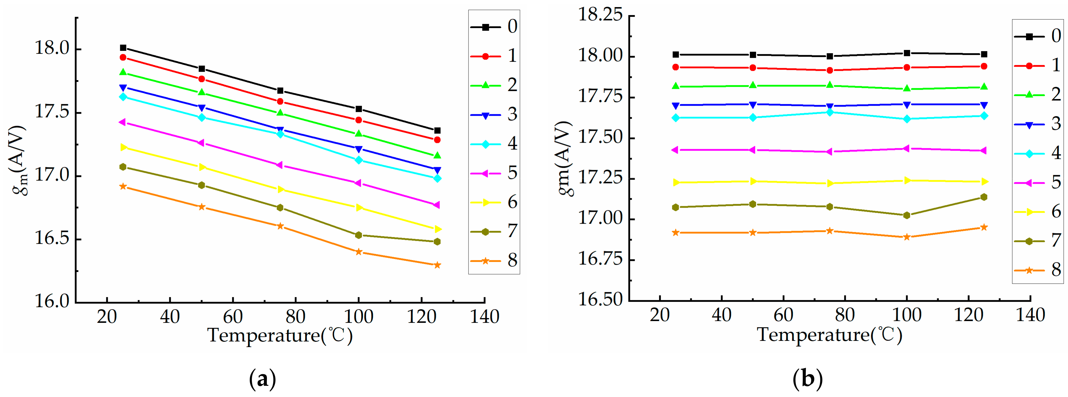
According to the above theoretical analysis and test results, it can be known that the chip failure and bond wire failure in the multi-chip IGBT module will cause the module transmission characteristic curve uGE-iC to change, and the module transconductance value calculated from the transmission characteristic curve can be used as characteristic parameters for health monitoring of the IGBT module. Since the temperature dependence of the module transconductance can conceal its fault characteristics or reduce its ability to monitor bond wire or chip faults, temperature calibration processing is required to eliminate temperature effects. The temperature-corrected module transconductance can effectively monitor chip failures and bond wire failures in IGBT modules.
For the IGBT module selected in this article, when one IGBT chip fails, the value of the module transconductance decreases by 6.243%. When two IGBT chips fail, the value of the module transconductance decreases by 12.472%. At this time, it can be basically determined that the IGBT module is in an aging failure state. It means that system failure will occur at any time, and the IGBT module should be repaired or replaced in time. If 70% of the bond wires on one IGBT chip fall off, it can be determined that the chip is close to aging failure [28]. When six bond wires in Chip 1 lift off, the value of the module transconductance is reduced by 3.721%, which means that Chip 1 is about to fail; when six bond wires lift off in Chip 2, the value of the module transconductance decreases by 10.286%, which means that the system is at risk of failure, Chip 2 is about to age and fail, and the module should be degraded or repaired.
Table 12 compares different state monitoring methods. Under the same test object and condition, the pre-threshold voltage VGE(pre-th) during the gate-emitter turn-on transient, collector-emitter voltage change rate dVCE/dt, and gate peak current IG(peak) have high sensitivity, but the three fault characteristic parameters are affected by temperature, and VGE(pre-th) and dVCE/dt cannot be used to monitor bond wire faults. dVCE/dt has a weak anti-interference ability. The IG(peak) measurement circuit needs to consider electromagnetic interference. The advantages of the method proposed in this article are as follows. (1) It can monitor chip faults and bonding wire faults at the same time, and it has good sensitivity. (2) This method has low sampling signal frequency and short measurement time, and it can ignore external heat sources and other electrical signals. It has a strong anti-interference ability such as the influence of external noise. (3) The parameter module mentioned in this article has a good linear relationship between the transconductance and temperature. This method is added to the temperature calibration process, which can be more accurately achieved under different junction temperatures IGBT module fault status monitoring. The method proposed in this paper can be used for in situ monitoring of the fault status of multi-chip parallel IGBT modules. It can be used to perform in situ monitoring when the converter is shut down (such as when the fan cuts off the wind speed, when the electric vehicle is stopped, etc.). Limitations and challenges include the stability of in situ monitoring devices, the lack of a standardized analysis of fault diagnosis, and condition assessment technology. However, this method cannot locate the specific location of chip faults and bond wire faults in the IGBT module and will continue to study the real-time online location and monitoring of IGBT module faults in the future.

6. Conclusions

This paper presents a method for monitoring the health of a multi-chip IGBT module based on module transconductance. According to the reliability model based on the module transconductance, the transmission characteristic curve of the selected IGBT module is measured in the test circuit, and its module transconductance value is calculated. The results show that the method can accurately identify the type of chip failure and the type of bond wire failure, and after temperature calibration, it can identify the aging failure process of the IGBT module without the influence of temperature. The method proposed in this article can simultaneously monitor the chip failure and the bond wire failure in the multi-chip IGBT module, and it is not affected by temperature. Compared with the existing monitoring method, it has better comprehensive characteristics, can realize the failure monitoring of the IGBT module, and improve the power inverter reliability.

Author Contributions

Conceptualization, methodology, software, validation, formal analysis, investigation, resources, C.W. (Chenyuan Wang) and Y.H.; data curation, writing—original draft preparation, C.W. (Chuankun Wang); writing—review and editing, X.W.; visualization, L.L. All authors have read and agreed to the published version of the manuscript.

Funding

This research was supported by the National Natural Science Foundation of China (Grant No. 51977153, 51977161, and 51577046), the State Key Program of National Natural Science Foundation of China (Grant No. 51637004), the national key research and development plan “important scientific instruments and equipment development” of China (Grant No.2016YFF0102200), the Equipment research project in advance of China (Grant No.41402040301).

Conflicts of Interest

The authors declare no conflict of interest.

References

  1. Schulze, H.; Niedernostheide, F.; Pfirsch, F.; Baburske, R. Limiting Factors of the Safe Operating Area for Power Devices. IEEE Trans. Electron Devices 2013, 60, 551–562. [Google Scholar] [CrossRef]
  2. Ghimire, P.; de Vega, A.R.; Beczkowski, S.; Rannestad, B.; Munk-Nielsen, S.; Thogersen, P. Improving power converter reliability: Online monitoring of high-power IGBT modules. IEEE Ind. Electron. Mag. 2014, 8, 40–50. [Google Scholar] [CrossRef]
  3. Wang, Z.; Qiao, W. An Online Frequency-domain Junction Temperature Estimation Method for IGBT Modules. IEEE Trans. Power Electron. 2015, 30, 4633–4637. [Google Scholar] [CrossRef]
  4. Bruckner, T.; Bernet, S. Estimation and Measurement of Junction Temperatures in a Three-level Voltage Source Converter. IEEE Trans. Power Electron. 2007, 22, 3–12. [Google Scholar]
  5. Eleffendi, M.A.; Johnson, C.M. Application of Kalman Filter to Estimate Junction Temperature in IGBT Power Modules. IEEE Trans. Power Electron. 2016, 31, 1576–1587. [Google Scholar]
  6. Choi, U.; Blaabjerg, F.; Jørgensen, S.; Munk-Nielsen, S.; Rannestad, B. Reliability Improvement of Power Converters by Means of Condition Monitoring of IGBT Modules. IEEE Trans. Power Electron. 2017, 32, 7990–7997. [Google Scholar]
  7. Beczkowski, S.; Ghimre, P.; de Vega, A.R.; Munk-Nielsen, S.; Rannestad, B.; Thogersen, P. Online Vce Measurement Method for Wear-out Monitoring of High Power IGBT Modules. In Proceedings of the 15th European Conference on Power Electronics and Applications (EPE), Lille, France, 2–6 September 2013; pp. 1–7. [Google Scholar]
  8. Smet, V.; Forest, F.; Huselstein, J.; Rashed, A.; Richardeau, F. Evaluation of Vce Monitoring as a Real-time Method to Estimate Aging of Bond wire-IGBT Modules Stressed by Power Cycling. IEEE Trans. Ind. Electron. 2013, 60, 2760–2770. [Google Scholar]
  9. Ji, B.; Pickert, V.; Cao, W.; Zahawi, B. In Situ Diagnostics and Prognostics of Wire Bonding Faults in IGBT Modules for Electric Vehicle Drives. IEEE Trans. Power Electron. 2013, 28, 5568–5577. [Google Scholar]
  10. Oh, H.; Han, B.; Mccluskey, P.; Han, C.; Youn, B.D. Physics-of-failure, Condition Monitoring, and Prognostics of Insulated Gate Bipolar Transistor Modules: A review. IEEE Trans. Power Electron. 2015, 30, 2413–2426. [Google Scholar]
  11. Singh, A.; Anurag, A.; Anand, S. Evaluation of Vce at Inflection Point for Monitoring Bond Wire Degradation in Discrete Packaged IGBTs. IEEE Trans. Power Electron. 2017, 32, 2481–2484. [Google Scholar]
  12. Eleffendi, M.A.; Johnson, C.M. In-service Diagnostics for Wire-bond Lift-off and Solder Fatigue of Power Semi-conductor Packages. IEEE Trans. Power Electron. 2017, 32, 7187–7198. [Google Scholar]
  13. Baker, N.; Dupont, L.; Munk-Nielsen, S.; Iannuzzo, F.; Liserre, M. IR Camera Calidation of IGBT Junction Temperature Measurement via Peak Gate Current. IEEE Trans. Power Electron. 2017, 32, 3099–3111. [Google Scholar]
  14. Baker, N.; Munk-Nielsen, S.; Iannuzzo, F.; Liserre, M. IGBT Junction Temperature Measurement via Peak Gate Current. IEEE Trans. Power Electron. 2016, 31, 3784–3793. [Google Scholar] [CrossRef]
  15. Mandeya, R.; Chen, C.; Pickert, V.; Naayagi, R.T. Prethreshold Voltage as A Low-component Count Temperature Sensitive Electrical Parameter without Self-heating. IEEE Trans. Power Electron. 2018, 33, 2787–2791. [Google Scholar] [CrossRef]
  16. Kexin, W.; Mingxing, D.; Linlin, X.; Jian, L. Study of bonding wire failure effects on external measurable signals of IGBT module. IEEE Trans. Device Mater. Reliab. 2014, 14, 83–89. [Google Scholar] [CrossRef]
  17. Mandeya, R.; Chen, C.; Pickert, V.; Naayagi, R.T.; Ji, B. Gate-Emitter Pre-threshold Voltage as a Health-Sensitive Parameter for IGBT Chip Failure Monitoring in High-Voltage Multichip IGBT Power Modules. IEEE Trans. Power Electron. 2019, 35, 9158–9169. [Google Scholar] [CrossRef] [Green Version]
  18. Du, M.; Kong, Q.; Ouyang, Z.; Wei, K.; Hurley, W.G. Strategy for Diagnosing the Aging of an IGBT Module by ON-State Voltage Separation. IEEE Trans. Electron. Devices 2019, 66, 4858–4864. [Google Scholar] [CrossRef]
  19. Musallam, M.; Johnson, C.M. Real-time Compact Thermal Models for Health Management of Power Electronics. IEEE Trans. Power Electron. 2010, 25, 1416–1425. [Google Scholar] [CrossRef]
  20. Hui, H.; Mawby, P.A. A Lifetime Estimation Technique for Voltage Source Inverters. IEEE Trans. Power Electron. 2013, 28, 4113–4119. [Google Scholar]
  21. Luo, H.; Chen, Y.; Sun, P.; Li, W.; He, X. Junction Temperature Extraction Approach with Turn-Off Delay Time for High-Voltage High-Power IGBT Modules. IEEE Trans. Power Electron. 2016, 31, 5122–5132. [Google Scholar] [CrossRef]
  22. Sun, P.; Gong, C.; Du, X.; Peng, Y.; Wang, B.; Zhou, L. Condition Monitoring IGBT Module Bond Wires Fatigue Using Short-Circuit Current Identification. IEEE Trans. Power Electron. 2017, 32, 3777–3786. [Google Scholar] [CrossRef]
  23. Chen, C.; Pickert, V.; Al-Greer, M.; Jia, C.; Ng, C. Localization and Detection of Bond Wire Faults in Multichip IGBT Power Modules. IEEE Trans. Power Electron. 2020, 35, 7804–7815. [Google Scholar] [CrossRef] [Green Version]
  24. Wang, K.; Zhou, L.; Sun, P.; Du, X. Monitoring Bond Wires Defects of IGBT Module Using Module Transconductance. IEEE J. Emerg. Sel. Top. Power Electron. 2020, in press. [Google Scholar] [CrossRef]
  25. Gao, B.; Yang, F.; Chen, M.; Ran, L.; Ullah, I.; Xu, S.; Mawby, P.A. Temperature Gradient-Based Potential Defects Identification Method for IGBT Module. IEEE Trans. Power Electron. 2017, 32, 2227–2242. [Google Scholar] [CrossRef]
  26. Hu, K.; Liu, Z.; Du, H.; Ceccarelli, L.; Iannuzzo, F.; Blaabjerg, F.; Tasiu, I.A. Cost-Effective Prognostics of IGBT Bond Wires with Consideration of Temperature Swing. IEEE Trans. Power Electron. 2020, 35, 6773–6784. [Google Scholar] [CrossRef]
  27. Li, Y. Research on Accelerated Aging and Aging Characteristic Parameters of IGBT Modules. Ph.D. Thesis, Chongqing University, Chongqing, China, 2018. [Google Scholar]
  28. Reigosa, P.D.; Wang, H.; Yang, Y.; Blaabjerg, F. Prediction of Bond Wire Fatigue of IGBTs in a PV Inverter Under a Long-Term Operation. IEEE Trans. Power Electron. 2016, 31, 7171–7182. [Google Scholar]
Figure 1. Insulated Gate Bipolar Transistor (IGBT) module structure and material coefficient of thermal expansion (CTEs).
Electronics 09 01559 g001
Figure 2. Internal structure diagram of multi-chip IGBT module.
Electronics 09 01559 g002
Figure 3. The physical diagram of the IGBT module and the internal equivalent circuit diagram of a single chip: (a) physical diagram; (b) equivalent circuit diagram.
Electronics 09 01559 g003
Figure 4. Transmission characteristic curve of the IGBT module before and after aging.
Electronics 09 01559 g004
Figure 5. Schematic diagram of failure monitoring: (a) Test circuit; (b) Measurement iC and uGE; (c) Acquisition of transmission characteristic curve.
Electronics 09 01559 g005
Figure 6. Transmission characteristic curves of IGBT modules under chip failure states.
Electronics 09 01559 g006
Figure 7. The relationship between IGBT module transconductance and temperature.
Electronics 09 01559 g007
Figure 8. Transconductance of the IGBT module with chip failure: (a) before temperature calibration (b) after temperature calibration.
Electronics 09 01559 g008
Figure 9. Transmission characteristic curves of Chip 1 under bond wire failure states.
Electronics 09 01559 g009
Figure 10. Transconductance of Chip 1 bonding wire fault module: (a) before temperature calibration and (b) after temperature calibration.
Electronics 09 01559 g010
Figure 11. The transmission characteristic curve of Chip 2 under bond wire failure states.
Electronics 09 01559 g011
Figure 12. Module transconductance of Chip 2 with bond wire failure: (a) before temperature calibration and (b) after temperature calibration.
Electronics 09 01559 g012
Table 1. Basic parameters of IGBT module.
Gate Voltage Source VGGInternal Gate Resistance RG(int)Gate-Emitter Capacitance CGEGate-Collector Capacitance CGCGate Inductance LG
±15 V2.16 mΩ8.8625 nF0.1375 nF12 nH
Table 2. Transconductance of IGBT modules under chip failure states.
Number of IGBT Chip FailuresIGBT Module Transconductance gm (A/V)Percentage Change (%)
019.18430
117.9982−6.243
216.8176−12.472
Table 3. Transconductance of the IGBT module in a healthy state at different temperatures.
Temperature (°C)IGBT Module Transconductance gm (A/V)
2519.1843
5019.0316
7518.8554
10018.6828
12518.5292
Table 4. Transconductance of IGBT modules under different temperatures and healthy states.
Number of IGBT Chip FailuresIGBT Module Transconductance gm (A/V)
T = 25 °CT = 50 °CT = 75 °CT = 100 °CT = 125 °C
019.184319.021218.855418.693718.5268
117.998217.832817.682317.513517.3416
216.817616.655316.487616.323116.1587
Table 5. Module transconductance under bond wire failure states of Chip 1.
Number of Chip 1 Bond Wires Lift-OffIGBT Module Transconductance gm (A/V)Percentage Change (%)
019.18430
119.0469−0.723
218.8914−1.542
318.8065−1.988
418.7641−2.211
518.6086−3.030
618.4774−3.721
718.3015−4.646
818.0772−5.827
Table 6. Module transconductance of Chip 1 in bond wire fault states at different temperatures.
Number of Bond Wires Lift-OffIGBT Module Transconductance gm(A/V)
T = 25 °CT = 50 °CT = 75 °CT = 100 °CT = 125 °C
i = 019.184319.018718.875418.675318.5412
i = 119.046918.885218.723118.549818.3864
i = 218.891418.731618.557618.413518.2418
i = 318.806518.645118.483218.321818.1517
i = 418.764118.593518.442618.268718.1102
i = 518.608618.450618.277518.117417.9483
i = 618.477418.307918.162117.978917.8235
i = 718.301518.142717.981217.805617.6518
i = 818.077217.918517.750917.590317.4186
Table 7. Module transconductance of Chip 1 bond wire fault state after temperature calibration.
Number of Bond Wires Lift-OffIGBT Module Transconductance gm (A/V)
T = 25 °CT = 50 °CT = 75 °CT = 100 °CT = 125 °C
i = 019.184319.182419.202819.166419.1960
i = 119.046919.048919.050519.040919.0412
i = 218.891418.895318.88518.904618.8966
i = 318.806518.808818.810618.812918.8065
i = 418.764118.757218.770018.759818.7650
i = 518.608618.614318.604918.608518.6031
i = 618.477418.471618.489518.470018.4783
i = 718.301518.306418.308618.296718.3066
i = 818.077218.082218.078318.081418.0734
Table 8. Module transconductance of Chip 2 under bond wire failure states.
Number of Bond Wires Lift-OffIGBT Module Transconductance gm (A/V)Percentage Change (%)
018.0147−6.156
117.9369−6.565
217.8167−7.198
317.7036−7.793
417.6258−8.203
517.4279−9.244
617.2299−10.286
717.0743−11.105
816.9188−11.924
Table 9. Module transconductance of Chip 2 with bond wire failure at different temperatures.
Number of Bond Wire Lift-OffIGBT Module Transconductance gm (A/V)
T = 25 °CT = 50 °CT = 75 °CT = 100 °CT = 125 °C
i = 018.014717.847917.675417.531617.3618
i = 117.936917.768217.589717.442917.2865
i = 217.816717.658117.496217.331517.1589
i = 317.703617.545417.370517.218317.0535
i = 417.625817.465117.332617.128716.9842
i = 517.427917.264517.089816.946516.7706
i = 617.229917.073116.895616.749816.5802
i = 717.074316.930516.751016.534516.4832
i = 816.918816.755416.603116.401016.2972
Table 10. Module transconductance of Chip 2 with bond wire failure after temperature normalization.
Number of Bond Wires Lift-OffIGBT Module Transconductance gm (A/V)
T = 25 °CT = 50 °CT = 75 °CT = 100 °CT = 125 °C
i = 018.014718.011618.002818.022718.0166
i = 117.936917.931917.917117.934017.9413
i = 217.816717.821817.823617.8022617.8137
i = 317.703617.709117.697917.709417.7083
i = 417.625817.628817.660017.619817.6390
i = 517.427917.428217.417217.437617.4254
i = 617.229917.236817.223017.240917.2350
i = 717.074317.094217.078417.025617.1380
i = 816.918816.919116.930516.892116.9520
Table 11. Verification of simulation results.
Number of Bond Wires Lift-OffTransconductance gm1 Experiment Results (A/V)gm1 Percentage Change (%)Transconductance gm2 Simulation Results (A/V)gm1 Percentage Change (%)
022.528019.1840
122.326−0.9019.047−0.723
222.259−1.2018.891−1.542
321.998−2.3518.807−1.988
421.730−3.5418.764−2.211
Table 12. Comparison of IGBT module chip fault monitoring methods.
Method1 Chip Failure70% of the Bonding Wires Fall OffAffected by TemperatureAnti-Interference Ability
VGE(pre-th)485 mV (8.182%)-yesstrong
dVCE/dt113.175 V/μs (7.545%)-yesweak
IG(peak)0.1734 A (−9.372%)0.04135 A (−2.235%)yesstrong
This article1.1861 A/V (−6.243%)0.7069 A/V (−3.721%)nostrong

