Abstract
In practice, the input filter is an important component in matrix converter (MC) systems for removing high harmonic components from input currents. Due to the input filter, the input power factor (IPF) at the main power supply does not always achieve unity. To investigate the behavior of the IPF, this paper analyzes the IPF compensation capacity of MCs with an LC input filter based on space vector theory and the conservation of energy law. The study shows that the range of voltage transfer ratio (VTR) to achieve unity IPF depends strongly on the quality factor, which is determined by the system parameters. If the quality factor is greater than 0.375, the MC can never achieve unity IPF for the whole range of VTR. If the quality factor is lower than 0.375, the MC can only achieve unity IPF for a certain range of VTR, except at a very low or very high VTR. Experimental results are provided to confirm the correctness of the study.
1. Introduction
A matrix converter (MC) is a type of direct ac–ac converter that can transfer input power to the output side directly without intermediate energy storage elements [1,2,3,4]. In recent years, MCs have received considerable research interest because they provide many attractive features compared with back-to-back converters, such as sinusoidal input/output waveforms, bidirectional energy-flow capability, controllable input-power factor (IPF), compact realization, high-temperature operating capability, and longevity [5,6,7,8]. With these potential advantages, MCs can be employed in specific industrial applications such as electric vehicles, military aircraft, and marine systems, where the converters are required to meet the demands of high-power density, reliability, and high-temperature operation [9,10]. To date, some commercial MC products have been launched by Yaskawa, Eupec, and Fuji companies [11,12,13].
An MC consists of nine bidirectional switches that connect any output phase directly to any input phase. In addition, an input filter is necessary to remove high harmonic components from the input currents and to meet electromagnetic interference (EMI) requirements at the MC’s input side [14,15,16]. Among many different topologies, the traditional second-order LC filter is most widely used [17]. To mitigate the oscillations around the LC resonance frequency, it is necessary to include a damping resistor in parallel with the inductor [18,19]. Figure 1 shows a common MC configuration, including the input filter.
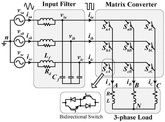
Figure 1.
A common matrix converter configuration.
However, the input filter can result in a displacement angle between the source voltage and source current, which causes an IPF degradation at the main power supply. Several IPF compensation algorithms have been proposed to improve the IPF for MCs [20,21,22,23]. Some papers have analyzed and compared many different control strategies regarding aspects including the IPF [24,25]. However, systematic investigation of the IPF compensation capability of MCs has not to date been presented in the literature.
To fulfil IPF control, this paper presents a study on the IPF compensation capacity of MCs. The IPF is analyzed with a traditional LC input filter (due to its widespread use). The analysis for other input filters is similar. The study is conducted using space vector theory and the conservation of energy law. The study of IPF compensation capability shows that MCs can only operate with unity IPF within a certain range of voltage transfer ratio (VTR). The IPF cannot reach unity at very low or very high VTR for every load value. In this case, the maximum achievable IPF versus VTR is presented. These results are useful for designing input filters and optimal IPF compensation algorithms for MCs. Experimental results carried out on an MC prototype with the traditional space vector modulation (SVM) method are presented to confirm the study.
The remainder of this paper is organized as follows. Section 2 briefly presents the traditional SVM method for MCs. Section 3 analyzes the input filter in MCs. Section 4 presents the principal study on the IPF compensation capability of MCs. Experimental results are provided in Section 5 to validate the study. Finally, Section 6 summarizes the contributions of this paper.
2. SVM Method for MCs
In a three-phase ac system, the source voltage is defined as follows:
The three instantaneous source voltages can be represented by the space vector :
Similarly, the space vectors of input voltage, output voltage, input current, and output current are defined, respectively, as follows:
Basically, the switching states of 9 bidirectional switches must satisfy the two main rules to provide safe operation of the MC: i) no short circuit at the input side, and ii) no open circuit at the output side.
As a result of these constraints, the three-phase MC has 27 possible switching states categorized into three groups as shown in Table 1:

Table 1.
Possible switching states in a matrix converter.
- (1)
- Group I includes 18 active-vector states,
- (2)
- Group II includes three zero-vector states,
- (3)
- Group III includes six rotating-vector states.
Conventionally, the rotating-vector states in Group III are not used to drive the MC, since their angular positions always change together with the input voltage making it difficult to create a repetitive pattern [6]. Therefore, in the traditional SVM method, active-vector states in Group I are selected to generate the desired output voltage vector [18], then zero-vector states are used to fulfil one sampling period.
For instance, when and are both in sector 1 as shown in Figure 2a,b, active-vector states among , and are selected to generate the reference output voltage vector . Meanwhile, from Figure 2b, to generate the input current vector in sector 1, active-vector states should be among and . Common states are chosen to generate both and in sector 1. Moreover, the states with higher magnitudes should be considered to maximize the capacity of the VTR. As can be seen from Figure 3, when the input current vector is in sector 1, two higher input line-to-line voltages are and . By looking up Table 1, it is, therefore, possible to conclude that four active-vector states (, , , and ) are selected to generate and in this case.
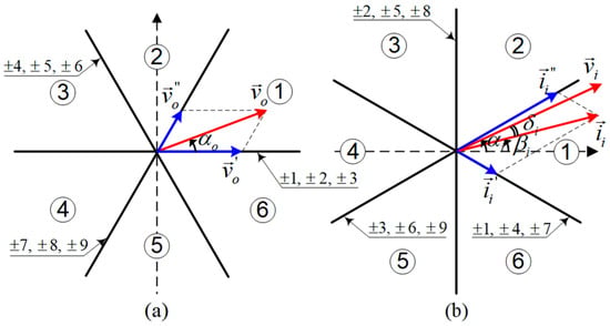
Figure 2.
The location of (a) the output voltage vector and (b) the input current vector.
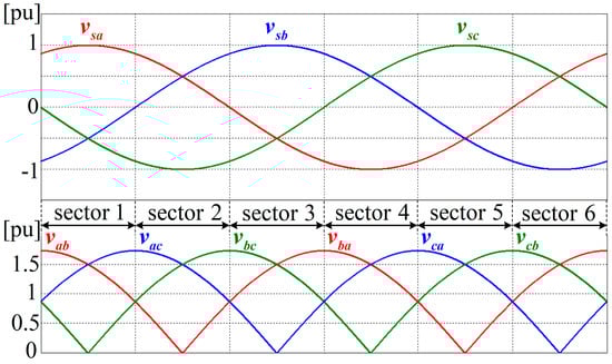
Figure 3.
Input phase and line-to-line voltages at main power supply.
Using the same procedure, the selected active-vector states for any combinations of output voltage and input current sectors are summarized in Table 2.
Table 2.
Selected active-vector states for each combination of output voltage and input current sectors in the traditional space vector modulation method.
Finally, zero-vector states are applied to fulfil the sampling period with the duty cycle:
All duty cycles must be non-negative and lower than or equal to unity:
Expressions (14) lead to the limit of the VTR in an MC:
From (15), the compensated angle is limited as follows:
3. Input Filter Analysis
In practice, the input filter is an essential component to smooth the input currents and to satisfy the EMI requirements at the MC’s input side [26]. Due to the input filter, the source current leads the source voltage at a high displacement angle, especially at light-load conditions, resulting in poor IPF. Therefore, to utilize maximum IPF at the main power supply, we need to investigate the displacement angle caused by the input filter.
Figure 1 shows a typical input filter configuration for MCs, namely, a second-order LC filter with a damping resistor and an inductor in parallel [16]. Figure 4 shows a simplified model of this input filter, from which the relationship between and is shown as follows:
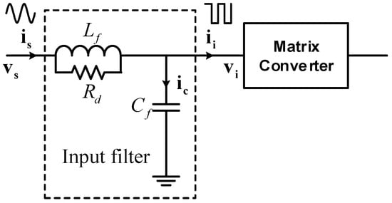
Figure 4.
Equivalent circuit of input filter.
To ensure sufficient damping of the input current and voltage oscillations, , so Equations (17) and (18) become (19) and (20), respectively, as follows:
Because the voltage drop across the input filter is very small compared with the source voltage, the input voltage of the MC and the source voltage are the same:
From Equations (19) and (21), the vector diagram of input voltages and currents is illustrated in Figure 5.
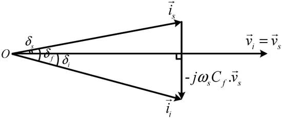
Figure 5.
Vector diagram of input voltages and currents.
To accomplish maximum achievable IPF at the main power source, we need to investigate the displacement angle between the MC input-current vector and the input-voltage vector , namely, .
4. Study on IPF Compensation
The conservation of energy law for MCs is expressed as follows:
where ; ; .
Therefore, from Equation (22), the source current amplitude is obtained as follows:
It should be noted that Equation (23) is true for any modulation case.
4.1. No Compensation
Figure 6 shows the vector diagram of input voltages and currents with no compensated angle, namely, . From Figure 6, it is possible to obtain the following relationship:
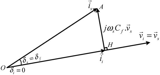
Figure 6.
Vector diagram of input voltages and currents with no compensated angle ().
From Equations (23) and (24), we can obtain the expression of displacement angle at the main power supply under the non-compensation condition as follows:
For each fixed value of VTR , is a constant value.
4.2. General Compensation
Figure 7 shows the vector diagram of input voltages and currents with the compensated angle δi = 0. We need to determine the displacement angle at the main power supply after applying a compensated angle δi between the MC input-current vector and input-voltage vector .
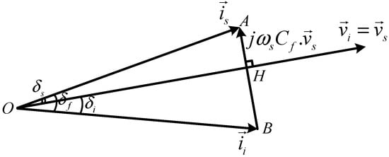
Figure 7.
Vector diagram of input voltages and currents with compensated angle .
From Equation (23), the power factor at the main power supply is always as follows:
Therefore, from Figure 7, the value of is:
From Figure 7, we can determine the relationship between and as follows:
When comparing Equations (25) and (28), the relationship between and becomes:
4.3. Unity IPF
From Equation (28), to achieve unity IPF at the main power source, namely, , the compensated angle must be as follows:
Let us define the quality factor for the IPF as follows:
From Equations (16), (30), and (31), the condition for achieving unity IPF is expressed as follows:
where .
Thus, from Equation (32), we can derive the following condition:
From Equation (33), it is possible to determine the VTR range to achieve unity IPF as follows:
under the following condition:
Figure 8, Figure 9 and Figure 10 present illustrations of the IPF at the main power supply when , , and , respectively. In Figure 8, when the quality factor is set to 0.1, the IPF at the main power supply can achieve unity in the range of . This result is in good agreement with the theoretical result in Equation (34). In Figure 9, when the quality factor is set to 0.375, the IPF at the main power supply can only achieve unity at . In Figure 10, when the quality factor is set to 0.54, the IPF at the main power supply cannot achieve unity within the entire range of VTR.
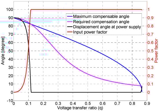
Figure 8.
Maximum allowable compensated angle, required compensation angle, displacement angle, and input power factor at the main power supple at .
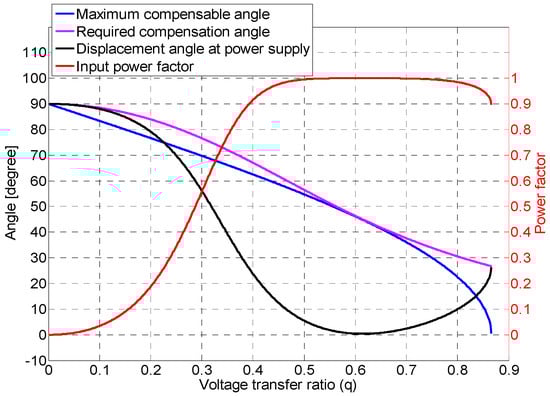
Figure 9.
Maximum allowable compensated angle, required compensation angle, displacement angle, and IPF at the main power supple at .
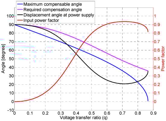
Figure 10.
Maximum allowable compensated angle, required compensation angle, displacement angle, and IPF at the main power supple at .
.
5. Experimental Results
To verify the effectiveness of the study, a prototype three-phase MC was used to supply a three-phase symmetrical passive RL load. The parameters used in the experiments are shown in Table 3. The MC was realized with 18 discrete IGBTs (IRG4PF50WD). The digital control system was implemented with fixed-point digital signal processors (TMS320F2812). A complex programmable logic device (EPM7128SLC84-15) was implemented for a four-step commutation. The input line-to-line voltages were sampled by voltage sensors (AD202) and a 12-bit A/D converter (AD7864).
Table 3.
System parameters.
As can be seen from Equation (35), the quality factor is a function of the output angular frequency , thus one easy way to change is to adjust . To verify the study, the quality factor is investigated at three values, i.e., lower than 0.375, equal to 0.375, and greater than 0.375. With reference to the values of the system parameters shown in Table 3, the MC is performed at , corresponding to the quality factor of 0.1, 0.375, and 0.54, respectively.
Figure 11, Figure 12 and Figure 13 show the input/output waveforms with no compensation at , , and , respectively. As can be seen, with no compensation, the source current inherently leads the source voltage with a certain angle due to the input filter. Figure 14, Figure 15 and Figure 16 show the input/output waveforms with maximum achievable IPF at , , and , respectively.
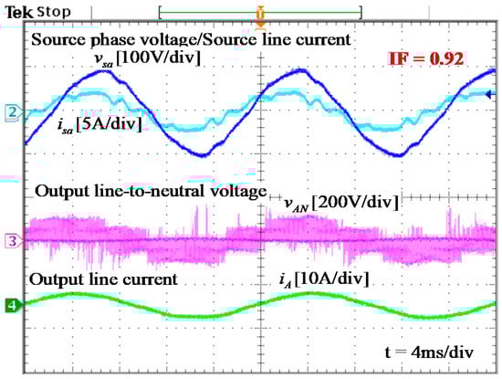
Figure 11.
Source phase voltage/source current, output line-to-neutral voltage, and output line current at with no compensation.
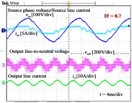
Figure 12.
Source phase voltage/source current, output line-to-neutral voltage, and output line current at with no compensation.
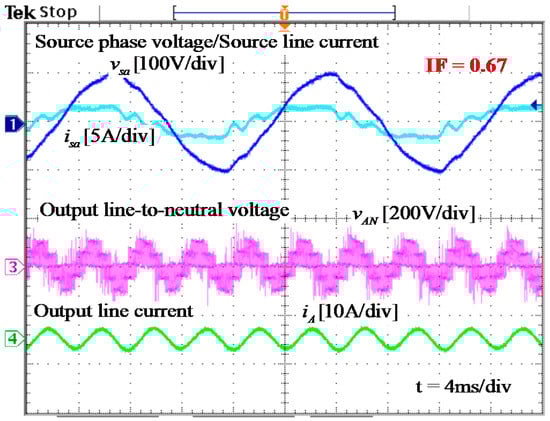
Figure 13.
Source phase voltage/source current, output line-to-neutral voltage, and output line current at with no compensation.
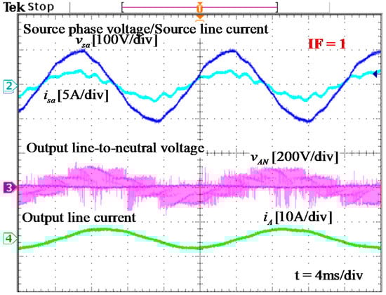
Figure 14.
Source phase voltage/source current, output line-to-neutral voltage, and output line current at with unity IPF compensation.
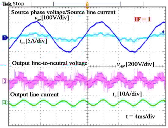
Figure 15.
Source phase voltage/source current, output line-to-neutral voltage, and output line current at with maximum compensated angle.
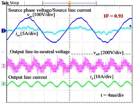
Figure 16.
Source phase voltage/source current, output line-to-neutral voltage, and output line current at with maximum compensated angle.
At Q = 0.1 < 0.375, from Equations (25) and (31), we can see that the displacement angle at low value of Q is also small and easy to be compensated, therefore, the IPF at the main power supply can be easily achieved unity. Figure 17 shows a comparison between IPF under no compensation and maximum compensated angle conditions at Q = 0.1. With maximum compensated angle condition, the MC can achieve unity IPF for a wide range of the VTR. This result is in good agreement with the theoretical study shown in Figure 8.
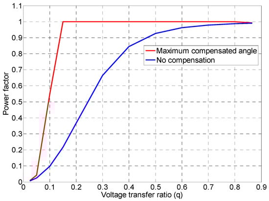
Figure 17.
Comparison between IPF under no compensation and maximum compensated angle conditions at .
At , the IPF at the main power supply can be achieved unity only at q = 0.6 as shown in Figure 18. At Q = 0.54 > 0.375, from Equations (25) and (31), the displacement angle at high value of Q is very large and difficult to be compensated, therefore, the IPF at the main power supply can never be achieved unity for entire range of the VTR as shown in Figure 19. These results are in good agreement with the theoretical results shown in Figure 9 and Figure 10.
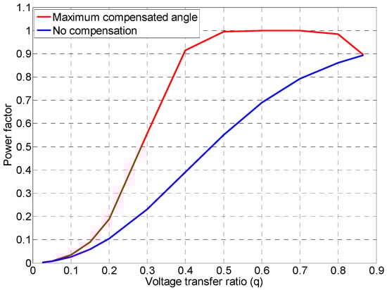
Figure 18.
Comparison between IPF under no compensation and maximum compensated angle conditions at .
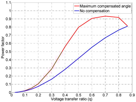
Figure 19.
Comparison between IPF under no compensation and maximum compensated angle conditions at .
The study shows that it difficult to achieve the unity IPF for MCs at high values of Q. From Equation (35), we can see that the value of Q is dependent on the input frequency, the input filter parameters, the output load parameters, and the output frequency. In practice, the input frequency and the input filter parameters are usually fixed, therefore, the value of Q is greatly dependent on the output load parameters and the output frequency. From this point of view, it is difficult to achieve the unity IPF when the MC operates at a high output frequency.
6. Conclusions
This paper has presented a study on the IPF compensation capacity of MCs with a traditional LC input filter. The study was defined by space-vector theory and the conservation of energy law. The study shows that the MC cannot always achieve unity IPF within the entire range of VTR, regardless of system parameters. The range of VTR for achieving unity IPF depends on the quality factor. The MC can achieve unity IPF for a wide range of VTR at a low-quality factor. The greater the quality factor, the narrower the range of VTR within which to achieve unity IPF. If the quality factor is greater than 0.375, the MC can never achieve unity IPF within the entire range of VTR. Experimental results verified that IPF behavior is in good agreement with the theoretical study.
Author Contributions
H.-N.N. established the major part of this paper, which includes study theory, doing experiment, and original draft preparation. M.-K.N. contributed to review and editing. T.-D.D. contributed to English revise. T.-T.T. contributed to doing experiment. Y.-C.L. provided resources and supervision. J.-H.C. provided resources and funding acquisition. All authors have read and agreed to the published version of the manuscript.
Funding
This research received no external funding.
Acknowledgments
This research was supported in part by the Korea Electric Power Corporation (Grant number: R18XA04). This work was supported by the Korea Institute of Energy Technology Evaluation and Planning (KETEP) and the Ministry of Trade, Industry & Energy(MOTIE) of the Republic of Korea (No. 2019381010001B).
Conflicts of Interest
The authors declare no conflict of interest.
Nomenclature
| Three-phase source voltage vector, | |
| , , | Instantaneous source phase voltages |
| Source voltage amplitude | |
| Angular frequency of source voltage | |
| Initial phase angle of source voltage | |
| Space vector of three-phase source voltage | |
| Space vector of three-phase source current | |
| Amplitude of source current, | |
| , , | Instantaneous input phase voltages of MC |
| , , | Instantaneous output phase voltages of MC |
| , | Amplitudes of MC input and output voltages |
| , | Phase angles of MC input and output voltages |
| , | Space vectors of MC input and output voltages |
| , , | Instantaneous input line currents of MC |
| , , | Instantaneous output line currents of MC |
| , | Amplitudes of MC input and output currents |
| , | Phase angles of MC input and output currents |
| , | Space vectors of MC input and output currents |
| Sampling period | |
| Duty cycles of zero and active vectors | |
| Voltage transfer ratio of MC, | |
| Output voltage sector | |
| Input current sector | |
| , | Inductance and capacitance of input filter |
| Damping resistance of input filter | |
| Displacement angle due to input filter, | |
| Compensated angle, | |
| Displacement angle at main power supply, | |
| Displacement angle at main power supply with no compensated angle | |
| Load displacement angle at output frequency, | |
| , , | Load resistance, inductance and impedance |
| Output frequency | |
| Output angular frequency |
References
- Empringham, L.; Kolar, J.W.; Wheeler, P.W.; Clare, J.C. Technological issues and industrial application of matrix converters: A review. IEEE Trans. Ind. Electron. 2013, 60, 4260–4271. [Google Scholar] [CrossRef]
- Kolar, J.W.; Friedli, T.; Rodriguez, J.; Wheeler, P.W. Review of three-phase PWM ac–ac converter topologies. IEEE Trans. Ind. Electron. 2011, 58, 4988–5006. [Google Scholar] [CrossRef]
- Villalba, L.R.M.; Lozano-Garcia, J.M.; Gutierrez-Torres, D.A.J.; Avina-Cervante, J.G.; Pizano-Martinez, A. Four-step current commutation strategy for a matrix converter based on enhanced-PWM MCU peripherals. Electronics 2019, 8, 547. [Google Scholar] [CrossRef]
- Nguyen, H.N.; Lee, H.H. A DSVM Method for Matrix Converters to Suppress Common-mode Voltage with Reduced Switching Losses. IEEE Trans. Power Electron. 2016, 31, 4020–4030. [Google Scholar] [CrossRef]
- Wheeler, P.W.; Rodríguez, J.; Clare, J.C.; Empringham, L.; Weinstein, A. Matrix converters: A technology review. IEEE Trans. Ind. Electron. 2002, 49, 276–288. [Google Scholar] [CrossRef]
- Rodriguez, J.; Rivera, M.; Kolar, J.W.; Wheeler, P.W. A review of control and modulation methods for matrix converters. IEEE Trans. Ind. Electron. 2012, 59, 58–70. [Google Scholar] [CrossRef]
- Nguyen, H.N.; Lee, H.H. An enhanced SVM method to drive matrix converters for zero common-mode voltage. IEEE Trans. Power Electron. 2015, 30, 1788–1792. [Google Scholar] [CrossRef]
- Friedli, T.; Kolar, J.W.; Rodriguez, J.; Wheeler, P.W. Comparative evaluation of three-phase ac–ac matrix converter and voltage dc-link back-to-back converter systems. IEEE Trans. Ind. Electron. 2012, 59, 4487–4510. [Google Scholar] [CrossRef]
- Nguyen, H.N.; Lee, H.H. A modulation scheme for matrix converters with perfect zero common-mode voltage. IEEE Trans. Power Electron. 2016, 31, 5411–5422. [Google Scholar] [CrossRef]
- Kwak, S.S. Investigation of fault-mode behaviors of matrix converters. J. Power Electron. 2009, 9, 949–959. [Google Scholar]
- Friedli, T.; Kolar, J.W. Milestones in matrix converter research. IEEJ J. Ind. Appl. 2012, 1, 2–14. [Google Scholar] [CrossRef]
- Zhang, J.; Li, L.; Dorrell, D.G. Control and applications of direct matrix converters: A review. Chin. J. Electr. Eng. 2018, 4, 18–27. [Google Scholar]
- Lei, J.; Feng, S.; Zhou, B.; Nguyen, H.; Zhao, J.; Chen, W. A simple modulation scheme with zero common-mode voltage and improved efficiency for direct matrix converter fed PMSM drives. IEEE J. Emerg. Sel. Topics Power Electron. 2019. [Google Scholar] [CrossRef]
- Nguyen, H.N.; Nguyen, T.D.; Lee, H.H. A modulation strategy to eliminate CMV for matrix converters with input power factor compensation. In Proceedings of the 42nd Annual Conference of the IEEE Industrial Electronics Society, Florence, Italy, 23–26 October 2016; pp. 6237–6242. [Google Scholar]
- Dasgupta, A.; Sensarma, P. Filter design of direct matrix converter for synchronous applications. IEEE Trans. Ind. Electron. 2014, 61, 6483–6493. [Google Scholar] [CrossRef]
- Varajao, D.; Araujo, R.E.; Miranda, L.M.; Lopes, J.A.P. EMI filter design for a single-stage bidirectional and isolated AC–DC matrix converter. Electronics 2018, 7, 318. [Google Scholar] [CrossRef]
- Klumpner, C.; Nielsen, P.; Boldea, I.; Blaabjerg, F. A new matrix converter-motor (MCM) for industry applications. In Proceedings of the Conference Record of the 2000 IEEE Industry Applications Conference, Thirty-Fifth IAS Annual Meeting and World Conference on Industrial Applications of Electrical Energy, Rome, Italy, 8–12 October 2000; Volume 3, pp. 1394–1402. [Google Scholar]
- Trentin, A.; Zanchetta, P.; Clare, J.; Wheeler, P. Automated optimal design of input filters for direct ac/ac matrix converters. IEEE Trans. Ind. Electron. 2012, 59, 2811–2833. [Google Scholar] [CrossRef]
- Sahoo, A.K.; Basu, K.; Mohan, N. Systematic input filter design of matrix converter by analytical estimation of RMS current ripple. IEEE Trans. Ind. Electron. 2015, 62, 132–143. [Google Scholar] [CrossRef]
- Nguyen, H.M.; Lee, H.H.; Chun, T.W. Input power factor compensation algorithms using a new direct-SVM method for matrix converter. IEEE Trans. Ind. Electron. 2011, 58, 232–243. [Google Scholar] [CrossRef]
- Schafmeister, F.; Kolar, J.W. Novel hybrid modulation schemes significantly extending the reactive power control range of all matrix converter topologies with low computational effort. IEEE Trans. Ind. Electron. 2012, 59, 194–210. [Google Scholar] [CrossRef]
- Li, X.; Su, M.; Sun, Y.; Dan, H.; Xiong, W. Modulation strategy based on mathematical construction for matrix converter extending the input reactive power range. IEEE Trans. Power Electron. 2014, 29, 654–664. [Google Scholar]
- Li, X.; Sun, Y.; Zhang, J.; Su, M.; Huang, S. Modulation methods for indirect matrix converter extending the input reactive power range. IEEE Trans. Power Electron. 2017, 32, 4852–4863. [Google Scholar] [CrossRef]
- Das, D.; Basak, A.; Mukherjee, K.; Syam, P. Degradation of input displacement power factor by input current filter and its compensation for a matrix converter. In Proceedings of the PEDES, Chennai, India, 18–21 December 2018. [Google Scholar]
- Malekjamshidi, Z.; Jafari, M.; Zhu, J.; Xiao, D. Comparative analysis of input power factor control techniques in matrix converters based on model predictive and space vector control schemes. IEEE Access. 2019, 7, 139150–139160. [Google Scholar] [CrossRef]
- Casadei, D.; Serra, G.; Trentin, A.; Zarri, L.; Calvini, M. Experimental analysis of a matrix converter prototype based on new IGBT modules. In Proceedings of the IEEE International Symposium on Industrial Electronics, Dubrovnik, Croatia, 20–23 June 2005; Volume 2, pp. 559–564. [Google Scholar]
© 2020 by the authors. Licensee MDPI, Basel, Switzerland. This article is an open access article distributed under the terms and conditions of the Creative Commons Attribution (CC BY) license (http://creativecommons.org/licenses/by/4.0/).