Article

Performance Degradation of Nanofilament Switching Due to Joule Heat Dissipation

by
Mohammad Shah Al-Mamun
and
Marius K. Orlowski
*
Bradley Department of Electrical and Computer Engineering, Virginia Polytechnic Institute and State University, Blacksburg, VA 24061, USA
*
Author to whom correspondence should be addressed.
Electronics 2020, 9(1), 127; https://doi.org/10.3390/electronics9010127
Submission received: 5 November 2019 / Revised: 15 December 2019 / Accepted: 5 January 2020 / Published: 9 January 2020
(This article belongs to the Section Microelectronics)

Abstract

:
When a memory cell of a Resistive Random Access Memory (ReRAM) crossbar array is switched repeatedly, a considerable amount of Joule heat is dissipated in the cell, and the heat may spread to neighboring cells that share one of the electrode lines with the heat source device. The remote heating of a probed memory cell by another cell allows separating the influence of temperature effects from the impact of the electric field on the resistive switching kinetics. We find that the cell-to-cell heat transfer causes severe degradation of electrical performance of the unheated neighboring cells. A metric for the thermal degradation of the I–V characteristics is established by a specific conditioning of a so-called “marginal” device used as a temperature-sensitive probe of electrical performance degradation. We find that even neighboring cells with no common metal electrode lines with the heated cell suffer substantial electrical performance degradation provided that intermediate cells of the array are set into a conductive state establishing a continuous thermal path via nanofilaments between the heated and probed cells. The cell-to-cell thermal cross-talk poses a serious electro-thermal reliability problem for the operation of a memory crossbar array requiring modified write/erase algorithms to program the cells (a thermal sneak path effect). The thermal cross-talk appears to be more severe in nanometer-sized memory arrays even if operated with ultra-fast, nanosecond-wide voltage/current pulses.

1. Introduction

Traditional non-volatile memory based on a floating gate MOSFET transistor reached its scaling limits and, hence, the development of alternative memory cells is imperative. Resistive random-access memory (ReRAM) is one of prime candidates to replace the current non-volatile technology due to its simple architecture, excellent scaling potential, low power consumption, high switching speed, large on/off ratio, and good retention and endurance properties [1,2,3]. Resistive memory cells also hold promise for neuromorphic applications [4,5]. The resistive switching device is a two-terminal device, such as Cu/TaOx/Pt, composed of a solid electrolyte insulating layer (here TaOx) sandwiched between two metal electrodes. The solid electrolyte layer displays a change between high and low resistance states in response to a suitably applied electric field. In so-called bipolar resistive devices, the transition from a low resistive state (LRS), characterized by the resistance Ron, to a high resistance state (HRS), characterized by the resistance Roff, occurs at an opposite polarity than the switching from HRS to LRS. The resistance switching effect is ascribed to the formation and rupture of conductive nanofilaments (CF) in the insulating material matrix due to ionic and charged defect electromigration, as well as to the thermal effects [6]. In the case of so-called electrochemical metallization [7] responsible for the formation of a metal atom CF, metal cations of the active electrode (here Cu) drift in the electric field toward the counter, also called the inert, electrode (here Pt), where they are stopped and neutralized. Over time, the Cu metal atoms pile up on the Pt interface and form a metal nanofilament between the two electrodes. This process constitutes the so-called SET operation. In contrast, when a negative voltage is applied to the active electrode, a large current flows through the filament, depositing Joule heat and causing the Cu atoms to diffuse out, leading to the rupturing of the filament at a critical current Ireset. The rupturing of the filament is called the RESET operation. In both SET and RESET operations, Joule heating is of crucial importance. It was amply demonstrated [8,9,10,11,12] that the RESET process is dominated by Joule heating. The self-heating effects associated with the switching of the cell lead to the deterioration of the Roff/Ron ratio [13], since, for the off-state associated with a semiconductor behavior, i.e., resistance, Roff decreases as the temperature increases, while the on-state exhibits metallic behavior with the resistance Ron increasing with increasing temperature. Walczyk et al. [13] found that the Roff/Ron ratio decreased from a value of 20 to approximately five over the temperature interval of 213–413 K. Such changes in Ron and Roff of ReRAM cells also cause significant degradation in the computational accuracy of ReRAM-based neuromorphic computing systems [5]. Specifically, a hotter cell is more susceptible to generating an incorrect output. The thermal reliability of ReRAM is also a concern for embedded memories for automotive applications [14]. Chang et al. [12] found two different modes of resistive switching for identical devices with the exception of a different thickness of the bottom Pt electrode. The difference in switching behavior was explained in terms of the temperature-dependent stability of the CF. Thinner thickness of the bottom electrode makes the dissipation of Joule heat less efficient and, hence, the filament is heated to a higher temperature and becomes more unstable at the same operation conditions than the device with a thicker Pt electrode.
Switching of a cell repeatedly leads to an increasing deposition of Joule heat in the device. Our results demonstrate that this Joule heat is transported preferentially along the electrode metal lines, affecting the neighboring cells disposed along the same electrode lines and causing the deterioration of their electrical properties. Due to this non-local cell heating configuration, the influence of temperature by dint of remote Joule heating of a heated cell and of the electric field on the switching kinetics of its neighbor cell could be studied separately. We found that even cells with no common metal lines with the heated cell are liable to thermal degradation provided that the intermediate cells are set into an on-state, thus establishing a continuous thermal pathway between the heated cell and the probed neighbor cell. A preliminary report of this work was submitted at the MRS Spring 2019 conference [15].

2. Device Fabrication and Electrical Characterization Methodology

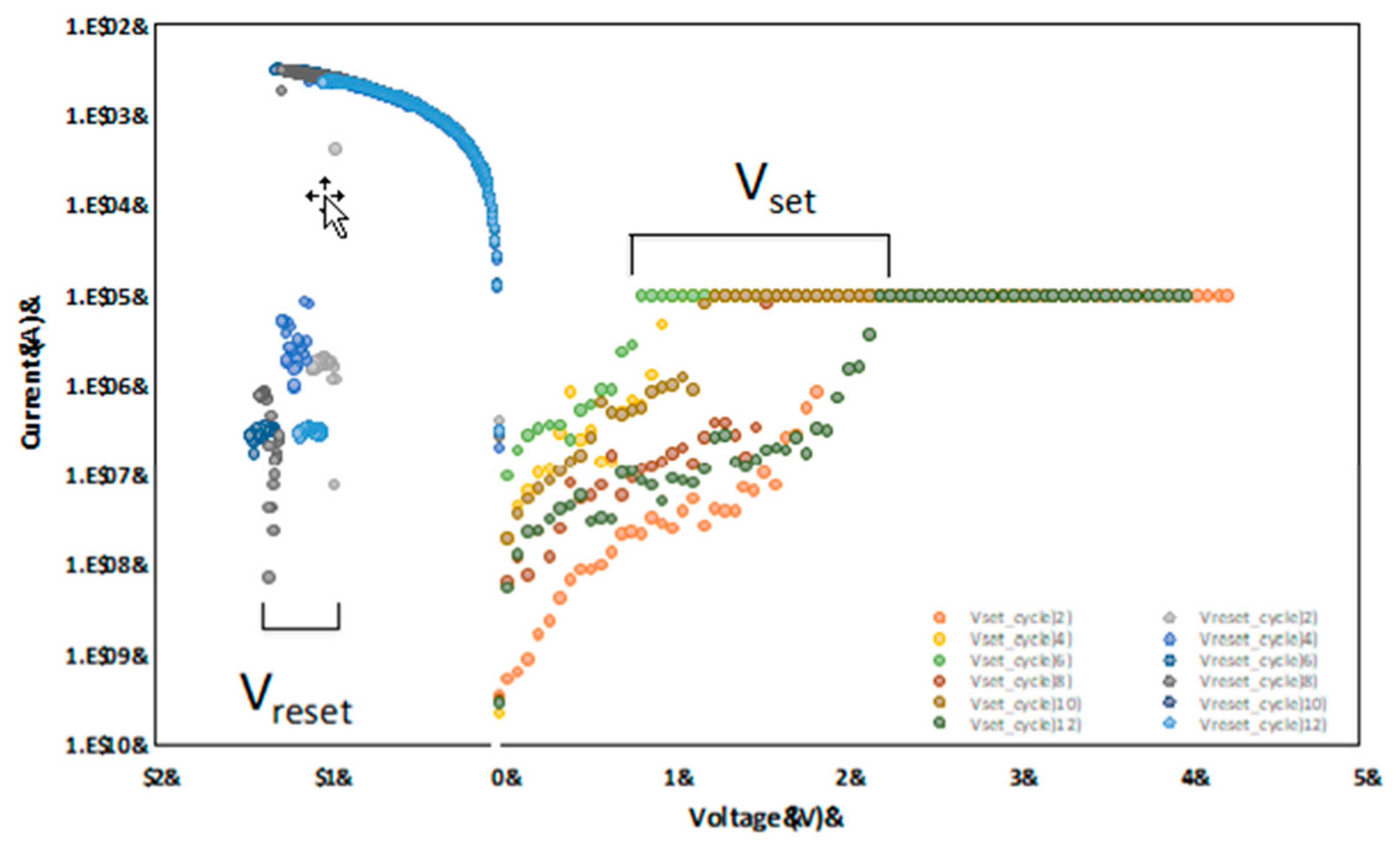
In the most common architecture, ReRAM cells lie at the intersection of perpendicular metal electrode lines in a crossbar array as shown in Figure 1a. The Cu/TaOx/Pt/Ti resistive RAM cells were fabricated in a crossbar array on a thermally oxidized Si wafer [3] with an SiO2 layer 730 nm thick. The cross-section of the resistive switching cell manufactured on an oxidized Si wafer is shown in Figure 1b. Cu (150 nm), Pt (50 nm), and Ti (20 nm) layers were deposited in a Kurt Lesker e-beam PVD-250 chamber and patterned by lift-off technology with a photoresist thickness of 2 μm to make sure that the sidewalls were sloped gently. A thin Ti layer of 20 nm was used between Pt and SiO2 to improve the adhesion of the Pt layer. The thickness of TaOx was 25 nm. The thickness of the TaOx on the sloped sidewalls of the Pt line was 98% of the planar thickness as confirmed by Ta2O5 atomic layer cells manufactured with Ta2O5 deposition by atomic layer deposition (ALD) [16]. The oxygen-deficient TaOx (x ≈ 1.9) was also deposited in the PVD-250 chamber by evaporating Ta2O5 pellets without O2 injection into the evaporation chamber. The details of the sample manufacturing process were given in Reference [16], where the role of the parameter x in TaOx (as opposed to the stoichiometric Ta2O5) on resistive switching properties was discussed in detail. The width of metal lines varies between 5 μm and 35 μm resulting in rectangular device areas of the device in the range of (5 to 5) × (35 to 35) μm2. The neighboring line pitch is between 155 μm and 185 μm. The memory cells used in this investigation were described in much detail in References [17,18]. The electrical characterization was performed at 300 K on a probe station equipped with a Keithley 4200-SCS. Before a measurement was taken, the two grounded needles were placed on the cell contacts for at least 20 s to make sure that the cell capacitor was fully discharged. Then, for the SET operation, the voltage of the Cu electrode starting at 0 V was ramped at a ramp rate (rr) ranging from 0.02 V/s to 2.00 V/s. During the SET operation, a compliance current (Icc) of 5 μA to 1 mA was imposed without an off-chip resistance, lest the device be damaged. A Cu conductive filament was established at a critical positive voltage Vset, and the conductive filament was ruptured at a negative voltage bias, when a critical voltage, denoted by Vreset, was reached. Typical I–V characteristics for a single cell are shown for the SET and RESET operations in Figure 2.

3. Thermal Cell-to-Cell Cross-Talk Effects in ReRAM Array

During the electrical characterization of the memory cells, it was noted that the electrical switching of a fresh cell A was degraded when a direct neighbor of cell A, cell B, was heated by repeated SET–RESET cycles. The degradation manifested itself by the onset of volatility after the device was cycled only a few times. This degradation of electrical properties disappeared when cell A was tested again after 10, 15, or 20 min or a longer cool-off time period. We assume that the thermally induced degradation subsided after times smaller than 5 min. Tests between various Pt and Cu lines proved that there are no sneak paths [19]. We hypothesize that the degradation of the electrical performance of the cell A was due to inter-cell thermal cross talk, which subsided within a few minutes when the heat was dissipated to the environment.

3.1. Definition of a “Marginal” Device as a Probe into Cross-Talk Effects

In order to quantify the thermal cross-talk, we fashioned a so-called “marginal” memory cell. By a cell being “marginal”, we mean following behavior of the cell after being subjected to a specific SET condition. We set a device at an Icc of only 10 μA and a voltage ramp rate rr = 1.1 V/s. When the cell was set in such conditions, the cell became volatile after a limited number of sequential SET–RESET switching cycles. One manifestation of volatility was spontaneous RESET events. The marginality of the device was demonstrated further when the device was set at slightly lower and slightly higher Icc. When applying Icc < 7 μA, the device could not be set permanently in an LRS state. When the same device was set at higher compliance currents of 8–10 μA, the LRS state was stable albeit only for a very small number of sequential switching cycles, typically 11–14, after which the cell eventually became volatile. A test was applied to ~100 cells set at Icc = 10 μA, and a maximum of consecutive switching cycles was determined. We obtained a mean of Mx = 12.7 cycles and standard deviation of σ = 1.3. A low rr = 0.1 V/s was applied during the RESET operation to allow for a long heating time. For a low rr, the current lingered for a long time and, hence, a low rr maximized heat dissipation. When the maximum number of switching cycles (Mx) was reached, the device was driven to highly unstable performance. On the other hand, a device set at Icc = 40–100 μA can be switched repeatedly more than 100 times. Thus, a “marginal” device demarcates the boundary between stable and unstable (volatile) behavior of the cell. Hence, a “marginal” device set at Icc = 10 μA was our “canary in the coal mine”, and the number of switching cycles, N < Mx, was our metric to quantify the degree of the thermal cross-talk. We found that such a marginal device when heated remotely by another cell would have a maximum number of switching cycles smaller than Mx = 13, depending by the amount of heating experienced by the cell. Thus, the measure N/Mx defines the onset of the cell’s volatility in response to the local temperature of the cell. The volatility is caused by the accumulated Joule heat during its consecutive switching. When such a probed cell is heated remotely from another (heated) cell, the temperature at which the cell becomes unstable should be reached after fewer I–V cycles. Thus, the remote heat superposes on the heat generated locally by the switching of the cell itself. In our experimental set-up, the time between heating cell B and characterization of probed cell A was about 50 s, i.e., the time required to replace manually the needles on the probe station.
When testing the first, second, third, and fourth neighboring cells in such a way, we found that the first neighbor suffered the highest degree of degradation yielding at most an N of three switching cycles, while the third and fourth neighbors were degraded only slightly, showing N of 9–11 compared with a mean of Mx = 13 for a fresh or thermally unaffected cell.

3.2. Dissipation and Transport of Joule Heat in ReRAM Arrays

At this point, it is instructive to estimate the heat dissipated in the cell during a single reset operation, characterized by a reset current Ires = Vres/Ron. Here, Ron is the resistance of the LRS state. The reset current is typically 1 mA < Ires < 6 mA. For a cell to which a constant voltage ramp rate is applied, the Joule heat QJH can be calculated using Equation (1).
Q J H = 0 t r e s V 2 ( t ) R o n d t = 0 V r e s / r r r r 2 × t 2 R o n d t = V r e s 3 × I c c 3 × r r × K
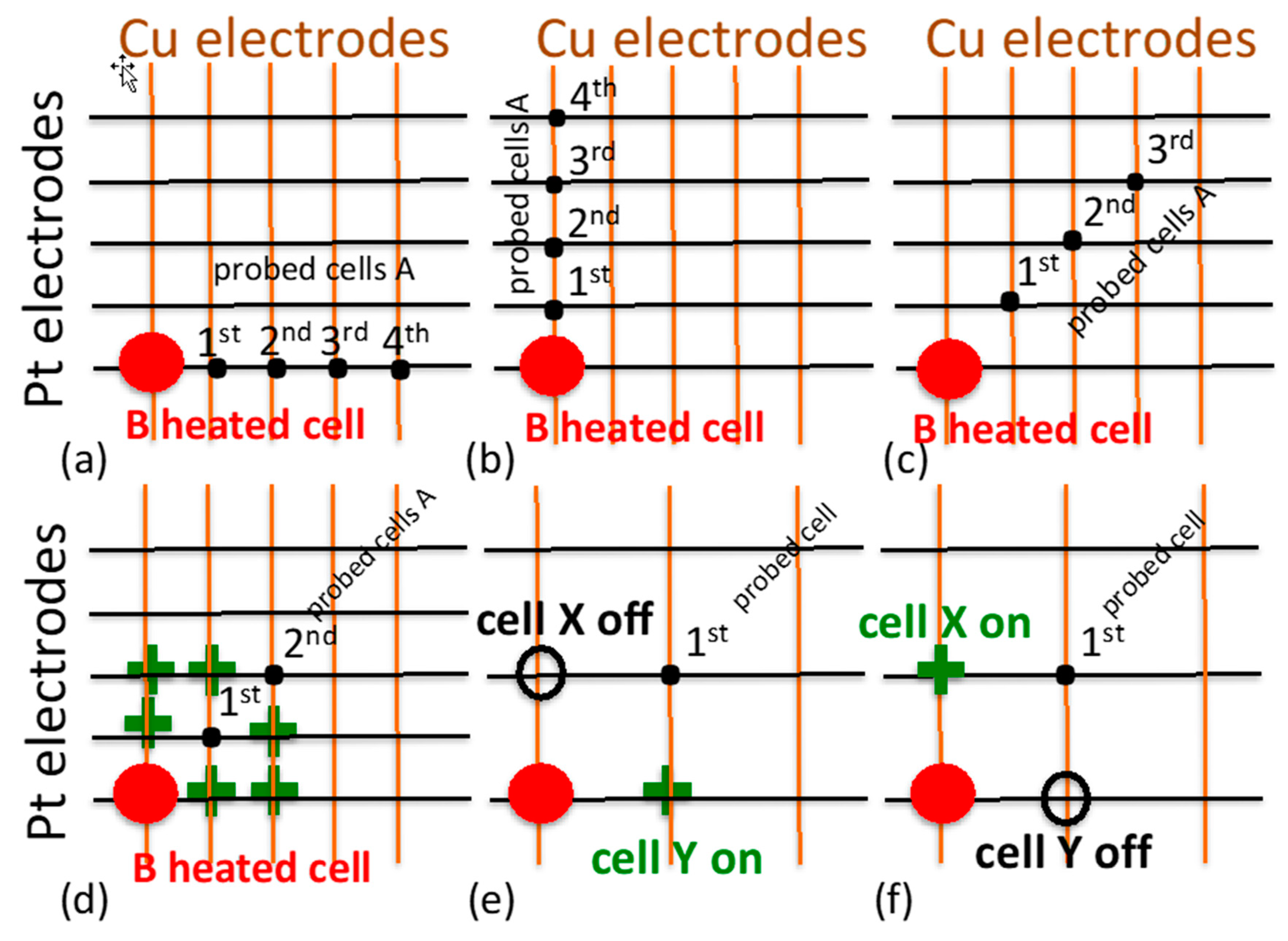
Here, the reset time tres at an applied voltage ramp rate rr is given by tres = Vres/rr [20,21]. In Equation (1), the well-known relationship between Ron device is described in terms of experimentally measurable parameters, namely, the compliance current Icc, the voltage ramp rate rr, and the reset voltage Vres. It was shown [22] that Ron depends on Icc via Ron = K/Incc with n ≈ 1 and K ≈ 0.2 V for Cu/TaOx/Pt devices. Depending on the chosen values for Icc and rr, QJH can vary from 3 to 60 μJ. When the cell is switched N times on and off repeatedly and in quick succession (50 s idle time between the set and reset operations), the total heat deposited in the cell is Qtot = N × QJH × f, where f is a dimensionless, positive number, less than unity, accounting for the heat removal out of the device between the subsequent switching events when the device is not electrically stressed. We estimate f to be between 0.6 and 0.85. The heat transferred to a neighboring cell n, as shown in Figure 3a,b, is then Qtran(n) = N × QJH × f × ttran(n), where the coefficient ttran(n) < 1 describes the efficiency of thermal transfer from the heat source cell B to the n-th neighboring cell A along one of the shared electrodes (Figure 3). Of course, ttran(n) > ttran(n + 1). Since the thermal conductivity of Cu (390 W/(mK)) and Pt (72 W/(mK)) is at least two orders of magnitude higher than the thermal conductivity of TaOx of 0.7 (W/(mK)) [23], it is clear that the dominant transport path to dissipate Joule heat takes place via the metallic connections within the crossbar array. Also, due to the thickness of the top Cu electrode of 150 nm (vs. 50 nm of the Pt electrode) and the finite size of the cell, the low thermal convection through air is very inefficient in dissipating the heat. Since the memory array was manufactured on a Si wafer with a grown field oxide of 650 nm thickness, it is reasonable to assume that the main heat transfer is achieved mainly via the metal electrode lines. The Cu filaments in the cells set to the on-state complement the network of electrode lines. Icc imposed at the SET operation of the intermediate cell can modulate the heat transport efficiency through its filament. High Icc leading to a low resistance filament provides a highly conductive thermal path between the Cu and Pt electrode. A low Icc provides an inefficient heat transport path because of the thinness of the filament and on account of a small thermal contact area with the Cu electrode.
Several thermal models exist in the literature describing the temperature distribution in ReRAM cells. Mickel et al. [24] established a geometrically equivalent circuit to describe the heat flows through a conductive filament, yielding temperature distribution of the memory cell. The critical temperature responsible for the rupturing of a filament was calculated to be ~1225 K. In another study, Mickel et al. [25] proposed a set of constitutive equations describing the evolution of heat transport. Based on this work, the temperature responsible for the rupturing of the filament can be as high as ~1500 K. Sun et al. [26] also found that the peak temperature of the filament was somewhere between 600 °C and 900 °C [26]. Thus, there is broad consensus that the local temperature of the filament is very high, and this temperature can only increase further when the cell is switched on and off sequentially and frequently.
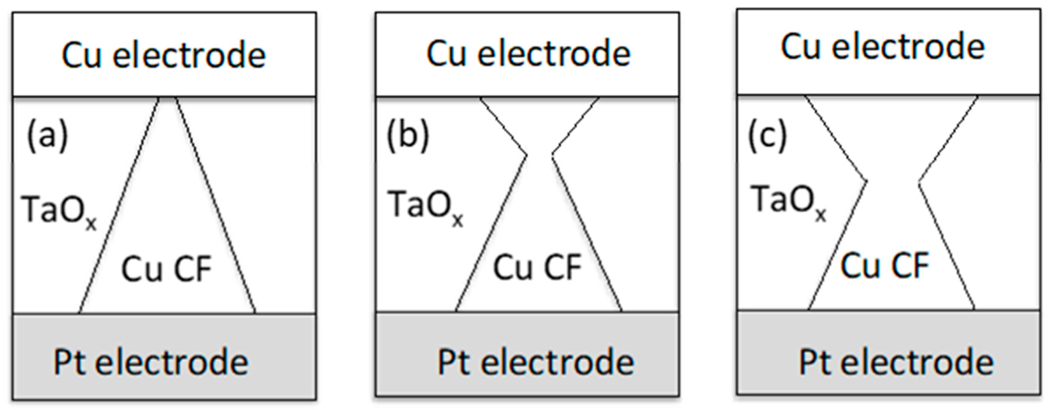
Since a weak filament is highly resistive with a constriction at the tip of the truncated cone-shaped filament, the area of contact formed with the Cu electrode is smaller than the area of contact with the Pt electrode (see Figure 4a). Hence, one would expect a more efficient heat transport from the filament to the Pt line rather than to the Cu line, despite the more than five-fold larger thermal conductivity of Cu than of Pt. Hence, based on this argument, one would expect that cells neighboring the heated cell and disposed on the Pt line should experience a larger heat transfer than the neighbors disposed along the Cu line. However, experimental data discussed below contradict such a conjecture.

3.3. Degradation of Electric Performance of Cells Sharing the Pt Electrode

We begin the discussion of the electrical degradation of the neighbor cells disposed along the Pt electrode line. They were characterized, one by one, immediately after heating by the heated cell marked by a red dot in Figure 3. The metric for degradation is established customarily by degradation defined in this context as
D = M x ( u n h e a t e d   c e l l ) N ( h e a t e d   c e l l ) M x ( u n h e a t e d   c e l l )
The mean of Mx for an unheated cell was found to be 13 SET–RESET cycles, as mentioned before. The cell degradation results for cells disposed along the Pt electrode are shown in Table 1 based on 66 devices measured. It can be seen that, for the nearest neighbors, the degradation was about D = 67%. In contrast, the degradation of the fourth device located on the Pt electrode was much smaller, D = 13%. The results could be explained by the heat transfer over a distance of n × 160 μm where n = 1, 2, 3, or 4, corresponding to the first, second, third, or fourth neighboring cell.
The switching behavior of cell A was impacted whenever a neighboring cell B (heat source device) went through repeated switching cycles. This means, quite surprisingly, that the thermal cross-talk was effective over distances of multiple integers of 160 μm. At the same time, this means that the electrode lines could not be assumed to be effective heat sinks, even for devices subject to no electrical stress. The heat transport over such large distances was further supported by the experimental dependence of the degradation effect on the width of the metal lines. For a wider Pt line (35 μm), the first neighbor was degraded much less N = 6 or D = (13 − 6)/13 = 54% than for a narrow Pt line (10 μm) cell, N = 3 or D = (13 − 3)/13 = 77%, as the heat was dissipated faster along the wider 35-μm line than along the 10-μm Pt line.

3.4. Degradation of Electric Performance of Cells Sharing the Cu Electrode

We turn our attention to the degradation behavior of cells A located along the Cu electrode that were neighbors of the heat source cell B. The neighbor cells of the heated memory cell disposed now along the Cu electrode (Figure 3b) were characterized analogously. The degradation results are summarized in Table 1 (Cu electrode) based on 53 tested cells. The degradation in terms of N for cells located on the Cu line was significantly larger than of those cells disposed on the Pt electrode. It can be observed that, for the Cu line, the distant neighboring cells were more severely degraded than those for the Pt electrode. Comparison of the fourth cell on the Pt electrode with the fourth cell on the Cu electrode shows that the degradation was five-fold larger for the Cu electrode. This appears to be consistent with the much better heat conductivity of Cu (385W/(mK) and 150 nm thick) lines than Pt (72 W/(mK) and 50 nm thick) lines, but is at odds with the assumptions of a much larger contact area of the Cu filament with the Pt than with the Cu electrode (see Figure 4a). As a general trend, we find for Cu line cells the same line width dependence as for the Pt lines discussed above; for a wide Cu line of 35 μm, the next neighbor is degraded much less than for a narrower Cu line of 10 μm. We also find that the coefficient ttrans for the Cu line is larger than for the Pt line due to larger electrode thickness and due to higher thermal conductivity of the Cu line than of the Pt line.

3.5. Degradation of Electric Performance of Cells with No Common Electrodes with the Heated Cell

Finally, we investigate the neighboring devices A that had neither Pt nor Cu electrode lines in common with the heated cell B. Figure 3c shows such three neighbor cells of the heated device that do not share any Pt and Cu electrodes with it. The cells in Figure 3c were electrically characterized under two different conditions: (1) the intermediate cells between the heated cell B and the tested cell A were in a non-conductive off-state, and (2) the intermediate cells were preset to a conductive on-state at Icc = 100 μA marked in Figure 3d by the green crosses. The Icc = 100 μA applied to the cells marked by green crosses ensured that a low-resistance Cu filament was formed with Ron typically between 450 Ω and 550 Ω. Such a low-resistance, robust conductive filament is assumed to provide a path of high thermal conductivity between Pt and Cu electrodes.
In the first case, as could be expected, we found no degradation of maximum switching cycles N for any of the diagonal neighbors of the heated device. This was expected since there was no thermally (metallic) conductive path between the heated cell B and the probed cell A. When, however, the cells marked by green crosses were preset to a conductive, i.e., LRS, state (see Figure 3d), the (diagonal) neighboring cell was found to be degraded considerably. A degradation of D = 19% was found for the first diagonal neighbor. The product of degradation 0.67 × 0.80 = 0.53 = 53% (see Table 1) is larger than 19% indicating that the Cu filament, despite its nanometer cross-section, provides an efficient conduit for heat transport, apparently by virtue of its very small length of 25 nm. It may be, therefore, concluded that the thermal cross-talk along the Cu electrode was 15-fold more efficient than along the Pt electrode.
It is known that the heat transport is proportional to the temperature gradient, to the wire cross-section, and to the thermal conductivity of the material, and it is inversely proportional to the length of the wire. The higher heat transport over the Cu line would indicate that the high conductivity of the Cu line more than compensated for the small contact area between the filament and the Cu electrode. The diameter of the filament, assumed to be of cylindrical shape for simplicity, was about 15 nm. When the thermal conductivity of the Cu filament is assumed to be roughly half of the thermal conductivity of bulk Cu, i.e., around 190 W/mK, then one could conclude that the heat transport via the 25-nm-long Cu filament is comparable with the heat transport along the Pt electrode over a distance of ~150 μm, assuming similar contact areas with the Cu and Pt electrodes.

3.6. Inference of the Nanofilament Shape

A more cogent explanation of the more efficient heat transport over the Cu line could be provided by assuming a revised shape of the Cu CF. Rather than a truncated cone shape, an hourglass shape is hypothesized for the Cu CF. A modified shape of the filament is shown in Figure 4b,c. For low Icc, the hourglass shape has a large base with the Pt electrode and a small base with the Cu electrode (Figure 4b). As the Icc increased, the base with Cu electrode grows while the base with Pt stays more or less constant (Figure 4c). The hourglass-shaped filament would be more consistent with our data as it provides now a larger contact area with the Cu electrode and would, thus, explain the large heat transport from the filament along the Cu electrode line to the neighboring cells along the Cu electrode. In the hourglass shape of the filament, its base with the Pt electrode is likely to be weakly dependent on the applied compliance current Icc, while the base of the hourglass with the Cu electrode should be a strong function of Icc.

4. Analysis and Implications for High-Pitch Nanometer-Sized Commercial Arrays

It should be noted that, in the case of the first diagonal device shown in Figure 3d, there exist two thermal conduction paths between the heated cell and the first diagonal cell. Evaluation of the electrical degradation of the first diagonal cell with intermediate cells partly in LRS and partly in HRS states, as shown in Figure 3e,f, reveals that the two individual paths contribute differently to the probed diagonal device’s electric degradation. The path first along the Cu and then along the Pt electrode (Figure 3e) causes a more severe degradation of the first diagonal cell than the conductive path first along Pt and then along the Cu electrode, as shown in Figure 3f. In the case of Figure 3e, the degradation of the first diagonal cell was 7%; in the case of Figure 3f, the degradation of the first diagonal device was 11%. This can be compared to the degradation of the second cells along the Cu and Pt lines, which were 75% and 53%, showing that the thermal connection via the Cu filament poses, despite good thermal conductivity, a heat transfer bottleneck when compared with the heat transport along the comparatively massive electrode lines. It can also be seen that the two paths contributed constructively (additively) to the overall degradation of (7% + 11%) ≈ 19%. These results demonstrate that a low-resistance Cu filament in cells X and Y provides an efficient thermal path to transmit the Joule heat to the diagonal cell. Testing the degradation of the neighbor cells as a function of the width of the metal lines, which in our case varied between 5 μm and 35 μm, we found that it took Joule heat less time to reach the fourth neighbor cell A for a 35-μm Cu line than for 5-μm or 10-μm Cu lines. This indicates that the heat was transmitted faster over or large distance of 700 μm by a wider Cu electrode line than by a narrow Cu electrode line.
At this point, the question arises as to how the present results apply to commercial ReRAM arrays that are a factor of 1000 smaller in geometrical dimensions than our memory cells, with correspondingly much tighter pitch to boot, and where the SET and RESET operations are performed with voltage and current pulses rather than by the relatively slow voltage or current ramps taking up to several seconds to successfully complete the operation. In commercial applications, a RESET voltage pulse is typically 5 V with a pulse width of a typically 200 ns [27]. Assuming a representative value for Ron = 2000 Ω, the Joule heat dissipated at the RESET QJHpulse = 200 ns × 52 V2/2000 Ω = 2.5 nJ. This is four orders of magnitude smaller than the Joule heat QJHramp dissipated at a ramped voltage given by Equation (1), which is typically 25 μJ. However, the commercial arrays are much smaller with a much tighter pitch. Therefore, consideration of the Joule heat density for both array cases can admits a meaningful comparison. For a commercial ReRAM array, we assume that, for an electrode thickness 50 nm, width 50 nm, and a pitch of 100 nm, we obtain a typical array unit volume of 2.5 × 10⁻¹⁶ cm3. We can now calculate the heat density for the commercial array in the vicinity of a reset cell as qcom = 2.5 nJ/2.5 × 10−16 cm3 = 107 J/cm3. In our university-fabricated memory arrays used in this work, the thickness and width of the Cu electrode were 150 nm and 10 μm, respectively, with a pitch of 160 μm that led to a corresponding volume of 2.4 × 10⁻¹⁰ cm3, six orders of magnitude larger than the corresponding volume for commercial memory arrays. With a switching Joule heat of 25 μJ, we obtained a heat density of qac = 105 J/cm3. Thus, the Joule heat density in commercial cutting edge arrays is two orders of magnitude higher than in our memory arrays.
This calculation indicates that, for commercial memory arrays, despite much lower switching Joule heat, the cell-to-cell thermal cross-talk poses a more serious conundrum because of the much smaller dimensions. There are two ways to mitigate the high heat density issue. Firstly, it can be done by reducing the generated Joule heat, and nip the problem in the bud, so to speak, at its origin, by lowering the reset current [28] or by using ultra-fast pulses of sub-ns widths [27]. The other possibility is an enhanced ability to remove the heat from the arrays quickly and efficiently. The heat dissipation could be increased by usage of metallic materials for the electrodes with higher thermal conductivity. One possibility would be to integrate the metal electrodes with graphene [29] which boasts a thermal conductivity of 3000–5000 W/(mK). However, higher thermal conductivity of the electrodes leads to another tradeoff; an electrode material of high thermal conductivity would induce a quicker heat dissipation of the heated device and allow a quicker return to non-degraded switching operation than an electrode material characterized by low thermal conductivity. A material with higher thermal conductivity, on the other hand, would transport the heat faster to the more distant cells in the crossbar array which then, in turn, would be affected more than in the case of a material with low thermal conductivity. Finally, we wish to mention that, in terms of heat transport modeling, our results indicate that the electrodes of the ReRAM cell cannot be treated as perfect heat sinks [8,30,31] especially when one cell is switched on and off repeatedly in rapid succession. Our results indicate that the local temperature of the metal electrode lines may considerably exceed the ambient room temperature assumed frequently in many thermal models of nanofilament heating.

5. Conclusions

In conclusion, we found that the heat deposited in a cell stressed by frequent switching is transported to the neighboring cells, causing their serious degradation in terms of electrical performance. Since the degradation of the cell performance occurs only when a cell nearby undergoes repeated switching cycles, its observed degradation, in the absence of other discoverable factors, was attributed to the impact of the heated cell in which heat is being dissipated over a number of switching cycles.
The neighbor cells disposed along one of the electrodes common with the heated device degrade the most. Cells with no electrode lines in common with the heated cell experience electrical degradation in terms of maximum switching cycles only in the case when an uninterrupted thermal (and, by the same token, electrical) path is provided between the probed neighbor and the heated cell. This occurs when the intermediate cells along the Cu and Pt line shared with the heated device (similar to the electric sneak path problem) are set into an LRS state. The electrical performance of a memory cell conditioned properly can be used as a probe into heat transfer phenomena. We find that the cell performance degradation is potentially more severe in nanometer-sized memory arrays despite much lower switching heat delivered by voltage or current pulses of ns widths.

Author Contributions

M.S.A.-M. manufactured the Cu/TaOx/Pt samples and performed electrical characterization of the cells. Both M.K.O. and M.S.A.-M. contributed to the theoretical explanations of the results and their implication for the reliability and performance of the ReRAM memory arrays. All authors have read and agreed to the published version of the manuscript.

Funding

This research has been partially funded by Semiconductor Research Consortium (SRC), grant number 444234.

Acknowledgments

Support of this research by Sean W. King of Intel Research Laboratories is gratefully acknowledged.

Conflicts of Interest

The authors declare no conflict of interest.

References

  1. Valov, I.; Waser, R.; Jameson, J.R.; Kozicki, M.N. Electrochemical metallization memories—fundamentals, applications, prospects. Nanotechnology 2011, 22, 254003. [Google Scholar] [CrossRef] [PubMed]
  2. Jeong, D.S.; Thomas, R.; Katiyar, R.S.; Scott, J.F.; Kohlstedt, H.; Petraru, A.; Hwang, C.S. Emerging memories: Resistive switching mechanisms and current status. Rep. Prog. Phys. 2012, 75, 076502. [Google Scholar] [CrossRef] [PubMed]
  3. Lee, M.J.; Lee, C.B.; Lee, D.; Lee, S.R.; Chang, M.; Hur, J.H.; Kim, Y.B.; Kim, C.J.; Seo, D.H.; Seo, S.; et al. A fast, high-endurance and scalable non-volatile memory device made from asymmetric Ta2O5−x/TaO2−x bilayer structures. Nat. Mater. 2011, 10, 625. [Google Scholar] [CrossRef] [PubMed]
  4. An, H.; Al-Mamun, M.S.; Orlowski, M.K.; Yi, Y. Learning Accuracy Analysis of Memristor-based Nonlinear Computing Module on Long Short-term Memory. In Proceedings of the International Conference on Neuromorphic Systems, Knoxville, Tennessee, 23–26 July 2018; ACM: New York, NY, USA, 2018. ISBN 978-1-4503-6544-4/18/07. [Google Scholar] [CrossRef]
  5. Beigi, M.V.; Memik, G. Thermal-Aware Optimizations of Reram-Based Neuromorphic Computing Systems. In Proceedings of the 55th Annual Design Automation Conference, San Francisco, CA, USA, 24–28 June 2018. [Google Scholar] [CrossRef]
  6. Liu, T.; Verma, M.; Kang, Y.; Orlowski, M. Volatile resistive switching in Cu/TaOx/δ-Cu/Pt devices. Appl. Phys. Lett. 2012, 101, 073510. [Google Scholar] [CrossRef] [Green Version]
  7. Kozicki, M.N.; Yun, M.; Hilt, L.; Singh, A. Applications of programmable resistance changes in metal-doped chalcogenides. J. Electrochem. Soc. 1999, 99, 298–309. [Google Scholar]
  8. Sun, P.; Lu, N.; Li, L.; Li, Y.; Wang, H.; Lv, H.; Liu, Q.; Long, S.; Liu, S.; Liu, M. Thermal crosstalk in 3-dimensional RRAM crossbar array. Sci. Rep. 2015, 5, 13504. [Google Scholar] [CrossRef]
  9. Mickel, P.R.; Lohn, A.J.; James, C.D.; Marinella, M.J. Isothermal switching and detailed filament evolution in memristive systems. Adv. Mater. 2014, 26, 4486–4490. [Google Scholar] [CrossRef]
  10. Russo, U.; Ielmini, D.; Cagli, C.; Lacaita, A.L. Self-accelerated thermal dissolution model for reset programming in unipolar resistive-switching memory (RRAM) devices. IEEE Trans. Electron Dev. 2009, 56, 193. [Google Scholar] [CrossRef]
  11. Ielmini, D. Modeling the universal set/reset characteristics of bipolar RRAM by field-and temperature-driven filament growth. IEEE Trans. Electron Dev. 2011, 58, 4309–4317. [Google Scholar] [CrossRef]
  12. Chang, S.H.; Chae, S.C.; Lee, S.B.; Liu, C.; Noh, T.W.; Lee, J.S.; Kahng, B.; Jang, J.H.; Kim, M.Y.; Kim, D.W.; et al. Effects of heat dissipation on unipolar resistance switching in Pt/NiO/Pt capacitors. Appl. Phys. Lett. 2008, 92, 183507. [Google Scholar] [CrossRef] [Green Version]
  13. Walczyk, C.; Walczyk, D.; Schroeder, T.; Bertaud, T.; Sowinska, M.; Lukosius, M.; Fraschke, M.; Wolansky, D.; Tillack, B.; Miranda, E.; et al. Impact of Temperature on the Resistive Switching Behavior of Embedded HfO2-Based RRAM Devices. IEEE Trans. Electron Dev. 2011, 58, 3124–3131. [Google Scholar] [CrossRef]
  14. Terai, M.; Saitoh, M.; Nagumo, T.; Sakotsubo, Y.; Yabe, Y.; Takeda, K.; Hase, T. High Thermal Robust ReRAM with a New Method for Suppressing Read Disturb. In Proceedings of the 2011 Symposium on VLSI Technology-Digest of Technical Papers, Honolulu, HI, USA, 14–16 June 2011. [Google Scholar]
  15. Al-Mamun, M.; Orlowski, M. Performance Degradation Due to Nonlocal Heating Effects in Resistive ReRAM Memory Arrays. MRS Adv. 2019, 4, 2593–2600. [Google Scholar] [CrossRef]
  16. Ghosh, G.; Kang, Y.; King, S.W.; Orlowski, M. Role of CMOS Back-End Metals as Active Electrodes for Resistive Switching in ReRAM Cells. ECS J. Solid State Sci. Technol. 2017, 6, N1–N9. [Google Scholar] [CrossRef]
  17. Kang, Y.; Liu, T.; Potnis, T.; Orlowski, M.K. Composite Cu/VO and VO/Cu Nanofilaments in Cu/Ta2O5/Pt Devices. ECS Solid State Lett. 2013, 2, Q54–Q57. [Google Scholar] [CrossRef]
  18. Liu, T.; Verma, M.; Kang, Y.; Orlowski, M.K. I-V characteristics of antiparallel resistive switching observed in a single Cu/TaOx/Pt cell. IEEE Electron Device Lett. 2012, 34, 108–110. [Google Scholar] [CrossRef]
  19. Linn, E.; Rosezin, R.; Kügeler, C.; Waser, R. Complementary resistive switches for passive nanocrossbar memories. Nat. Mater. 2010, 9, 403–406. [Google Scholar] [CrossRef]
  20. Ghosh, G.; Orlowski, M. Write and Erase Threshold Voltage Interdependence in Resistive Switching Memory Cells. IEEE Trans. Electron Dev. 2015, 62, 2850–2856. [Google Scholar] [CrossRef]
  21. Ghosh, G.; Orlowski, M.K. Correlation between set and reset voltages in resistive RAM cells. Curr. Appl. Phys. 2015, 15, 1124–1129. [Google Scholar] [CrossRef]
  22. Liu, T.; Kang, Y.; El-Helw, S.; Potnis, T.; Orlowski, M. Physics of the voltage constant in multilevel switching of conductive bridge resistive memory. Jpn. J. Appl. Phys. 2013, 52, 084202. [Google Scholar] [CrossRef]
  23. Landon, C.D.; Wilke, R.H.; Brumbach, M.T.; Brennecka, G.L.; Blea-Kirby, M.; Ihlefeld, J.F.; Marinella, M.J.; Beechem, T.E. Thermal transport in tantalum oxide films for memristive applications. Appl. Phys. Lett. 2015, 107, 023108. [Google Scholar] [CrossRef]
  24. Mickel, P.R.; Lohn, A.J.; Marinella, M.J. Detection and characterization of multi-filament evolution during resistive switching. Appl. Phys. Lett. 2014, 105, 053503. [Google Scholar] [CrossRef]
  25. Mickel, P.R.; Lohn, A.J.; Marinella, M.J. Memristive switching: Physical mechanisms and applications. Mod. Phys. Lett. B 2014, 28, 1430003. [Google Scholar] [CrossRef]
  26. Sun, P.; Li, L.; Lu, N.; Li, Y.; Wang, M.; Xie, H.; Liu, S.; Liu, M. Physical model of dynamic Joule heating effect for reset process in conductive-bridge random access memory. J. Comp. Electron. 2014, 13, 432–438. [Google Scholar] [CrossRef]
  27. Yang, X. Demonstration of Ultra-Fast Switching in Nanometallic Resistive Switching Memory Devices. J. Nanosci. 2016, 8132701. [Google Scholar] [CrossRef] [Green Version]
  28. Lanza, M. A Review on Resistive Switching in High-k Dielectrics: A Nanoscale Point of View Using Conductive Atomic Force Microscope. Materials 2014, 7, 2155–2182. [Google Scholar] [CrossRef]
  29. Al-Mamun, M.S.; Orlowski, M. Quick heat dissipation in ReRAM with graphene engineered electrodes. In preparation.
  30. Lohn, A.J.; Mickel, P.R.; Marinella, M.J. Analytical estimations for thermal crosstalk, retention, and scaling limits in filamentary resistive memory. J. Appl. Phys. 2014, 115, 234507. [Google Scholar] [CrossRef]
  31. Niraula, D.; Karpov, V.G. Heat transfer in filamentary RRAM devices. IEEE Trans. Electron Dev. 2017, 64, 4106. [Google Scholar] [CrossRef] [Green Version]
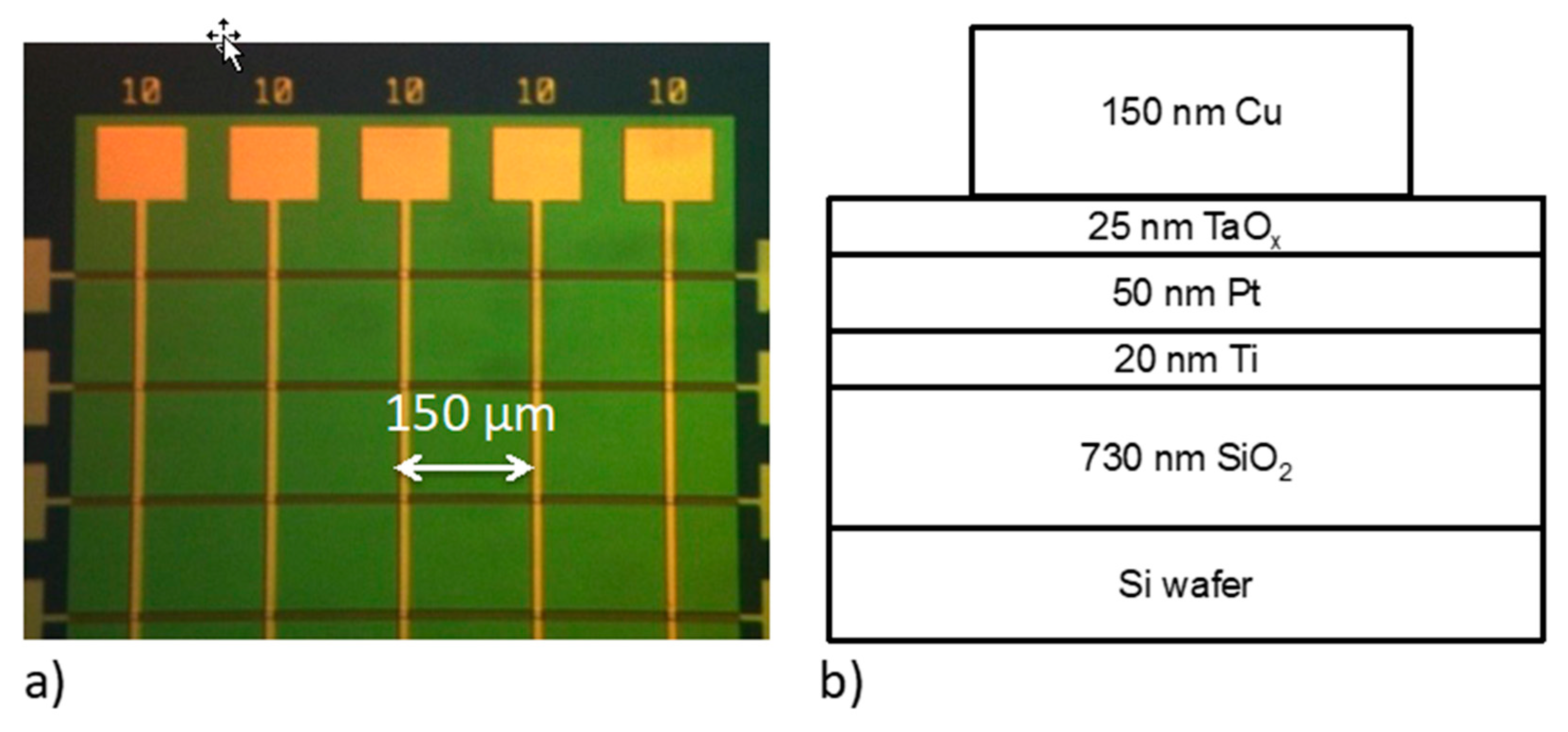
Figure 1. (a) Optical micrograph of the crossbar architecture of Cu/TaOx/(Pt and Ru) devices; (b) cross-section of the device with relevant layer thicknesses indicated.
Electronics 09 00127 g001
Figure 2. Even cycles of the typical first 12 switching set and reset cycles of a Cu/TaOx/Pt device.
Electronics 09 00127 g002
Figure 3. Location of neighbor cells relative to the heated cell marked by a red dot. Initially, the cells are set in an off-state. (a) Heat transport from the heated cell to its neighbors located on the Pt electrode. (b) Heat transport to its neighbors disposed along the Cu electrode. (c) Heat transport to its neighbors located diagonally with respect to the heated cell. (d) Heat transport to its neighbors at diagonal locations with intermediate cells (marked by green crosses) in the on-state. (e) Thermal path from the heated cell to first cell via cell Y. (f) Thermal path from the heated cell to first cell via cell X.
Electronics 09 00127 g003
Figure 4. Different geometrical shapes approximating the hypothesized form of a Cu filament: (a) conventionally assumed shape of a truncated cone; (b) an hourglass-shaped filament formed at low Icc; (c) an hourglass-shaped filament formed at high Icc.
Electronics 09 00127 g004
Table 1. Degradation D of the neighbor cells of the heated device.
Neighbor Cell to the Heated Cell Along Pt Metal LineNeighbor Cell to the Heated Cell Along Cu Metal Line
#neighbor1st2nd3rd4th1st2nd3rd4th
D [%]6753401380757067