Article

Parameters Design and Optimization of a High Frequency, Interleaved, Dual-Buck, Bidirectional, Grid-Connected Converter

School of Electrical and Information Engineering, Tianjin University, Tianjin 300072, China
*
Author to whom correspondence should be addressed.
Electronics 2019, 8(9), 973; https://doi.org/10.3390/electronics8090973
Submission received: 9 August 2019 / Revised: 26 August 2019 / Accepted: 29 August 2019 / Published: 31 August 2019
(This article belongs to the Special Issue Smart Energy Storage Systems)

Abstract

:
In this paper, a high frequency, interleaved, dual-buck, bidirectional, grid-connected converter topology is proposed. Free from the straight-through and dead-time distortion issues, both higher switching frequency and power density can be achieved. Due to the interleaved technique, the current ripple and stress for inductors and other power devices can be effectively reduced. Moreover, a novel filter parameter design method is proposed. The method is optimized with smaller inductance, higher filtering performance, and better steady-state performance. For one thing, the performance requirements under the two states of inverter and rectifier are comprehensively considered. For another, the relationship between the performance indexes and the filter parameters is analyzed. However, the results show that the relationship between the performance indexes is contradictory. A set of optimization parameters were obtained by setting the priority of the filter performance index. The specific design process of the filter parameters is given in detail. In order to verify the rationality of the parameter design, a 5 kW prototype was built and tested. The total harmonic distortions (THDs) of the grid currents in the among grid-connected inverter, off-connected inverter, and rectifier states under full load were 2.7%, 1.2%, and 4.5%, respectively, and the power density reached 36 W/in3.

1. Introduction

Energy storage units are widely used in distributed new energy, grid-connected power generation systems. On one hand, they reduce the power fluctuation of power grid systems. On the other hand, they improve the friendliness of the energy interaction between the users and grid. However, the efficiency and power density of the energy storage unit needs to be further improved [1,2,3]. Therefore, as the interface circuit of distributed energy storage units, the grid-connected converter needs to highlight two aspects of performance: (1) High efficiency to achieve the bidirectional flow of energy. (2) Smaller volume and lower weight. According to the research of relevant scholars, the methods of improving power density are as follows: (1) To increase the working frequency and reduce the size of the filter. (2) To design the filter parameters reasonably and to reduce the nominal value of the filter elements to achieve a higher power density [4,5,6,7,8,9,10].
Increasing the operating frequency of the converter can greatly reduce the size of the inductors and capacitors. Thereby, the power density of the converter is improved. However, the traditional bridge-based converter needs to inject dead-time, which limits the increase of the operating frequency. Further, the dead-time will lead to more waveform distortion. Therefore, compared with the traditional bridge circuit, the new type of grid-connected converter without straight-through (i.e., without injecting dead zone) has certain research value. References [11,12] present a dual-buck, bridge-less inverter topology, which overcomes the problem of straight-through without injecting dead-time. It is beneficial to realize high operating frequency of the converter. Reference [13] proposes a dual-input, dual-buck, bridge-free topology without dead-zone distortion. It greatly reduces the injection of low-order harmonics and has a high power factor. Reference [14] proposes a dual-output, dual-buck converter, which improves the load capacity while retaining the advantages of the buck converter. Reference [15] introduces an interleaved technology on the basis of a dual-buck converter to further reduce the inductance current ripple. It reduces the size of the filter and improves the power density of the converter. In the above literatures, dual-buck, bridge-free topology is used to effectively eliminate the problem of straight-through, reduce the injection of low-order harmonics, and significantly improve the quality of circuit waveforms. In addition, most of the converters use SiC devices, which effectively improves the switching frequency. However, the above literatures only discuss unidirectional power flow and do not involve bidirectional power flow. Therefore, the research on bidirectional, grid-connected converters still needs to be carried out.
Moreover, a series of research work about the design method of filter parameters has been carried out. In references [16,17], the inductance and capacitance of the filter were obtained by preset ripple, reactive power limitation, and resonant frequency. The design method was simple, feasible, and easy to calculate. However, the constraints among the filter parameters were not considered, which has a certain impact on the performance of the filter. Reference [18] comprehensively considered the relationship between the attenuation of resonant peaks and circuit losses and achieved the design of filter parameters. This design method improves the stability of the converter, however the introduction of filter resistance will have a certain impact on the efficiency. Reference [19] designed the filter parameters according to the relationship between filter parameters and total harmonic distortion (THD) and achieved a better filtering effect. In reference [20], the parameters of the filter were designed by using the restriction of the resonant frequency of the filter. The design method takes into account the harmonic suppression ability and the stability of the system and has high practicability. However, references [19,20] did not fully consider the relationship between filter parameters and performance indexes. Reference [21] synthetically considered the performance indexes of the filter and drew the relationship curves between the filter parameters and the performance indexes. The design method is more intuitive, however the process is more complicated. In the above literatures, the design of the filter is based on the characteristics of the circuit and the design objectives are clear and the design method is feasible. However, most of the above literatures take single performance as the optimization target and do not consider the constraints between various performances. Thus, it is difficult to take into account multiple performance requirements at the same time. What is more, the power density of the converter is not taken as the optimization target. In addition, the above parameter design methods are discussed on the basis of unidirectional power flow, which has not been extended to the case of bidirectional power flow and has certain limitations. Therefore, it is of great importance to study the design method of bidirectional converter filter parameters.
In this paper, based on SiC power devices, a high frequency, interleaved, dual-buck, bidirectional, grid-connected converter is proposed. The topology has two states: inverter state and rectifier state. Firstly, model analysis of the two states will be carried out in Section 2. Then, a parameter design method considering the performance requirements of both the inverter and rectifier states will be proposed in Section 3. In this method, the coupling relationship between the filter parameters and performance indexes is considered comprehensively. Taking power density, filtering performance, and stability as optimization targets, a set of reasonable parameters are obtained by setting a target priority. Finally, an experimental prototype with a rated power of 5 kW is built to verify the theoretical analysis in Section 4.

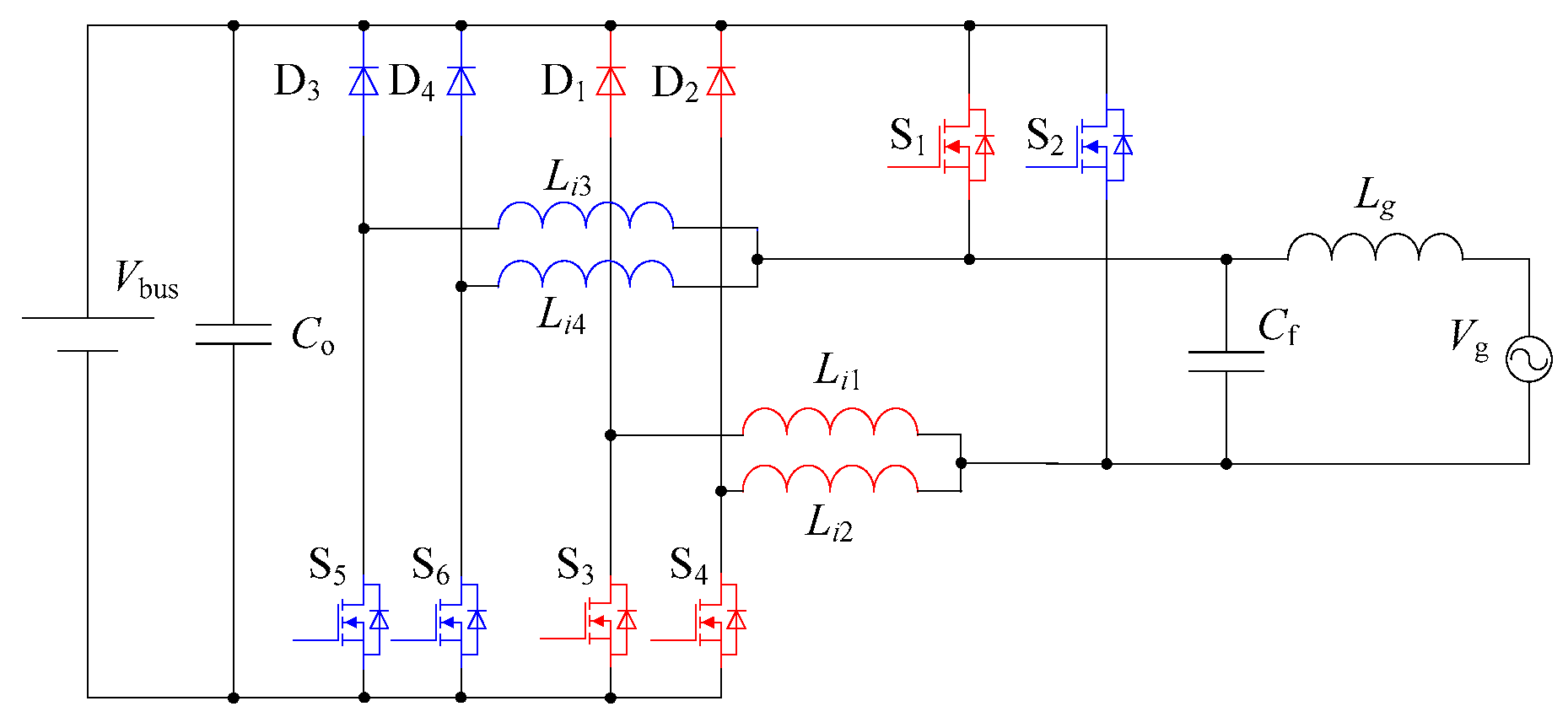
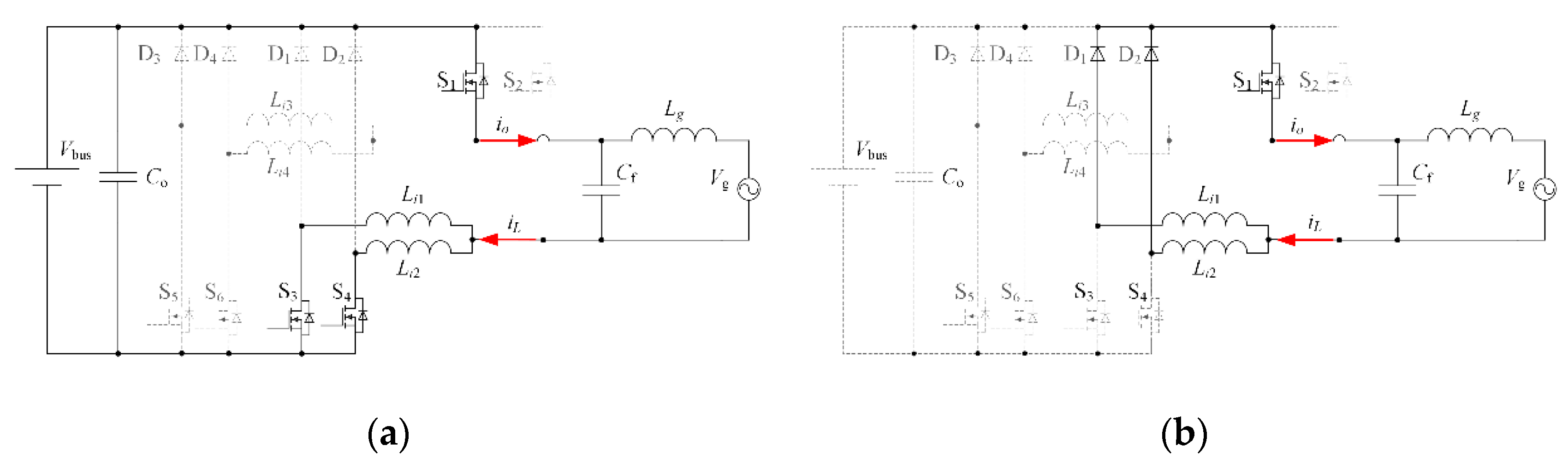
2. Topology Description and Operation Principles

2.1. Topology Description

The topology of the proposed interleaved, dual-buck, bidirectional, grid-connected converter is illustrated in Figure 1, which includes the inverter state and the rectifier state. In the inverter state, the circuit consists of four identical Buck circuits: S1, S3, D1, and Li1 form Buck1; S1, S4, D2, and Li2 form Buck2; S2, S5, D3, and Li3 form Buck3; and S2, S6, D4, and Li4 form Buck4. The driving signal of switch S3 of Buck1 leads that of switch S4 of Buck2 by 180 degrees, which constitutes inverter interleaving unit 1. The driving signal of switch S5 of Buck3 leads that of switch S6 of Buck4 by 180 degrees, which constitutes inverter interleaving unit 2. In a grid line period, two groups of inverter interleaving units work alternately in each half cycle to realize the inverter function.
In the rectifier state, the circuit consists of four identical Boost circuits: S5, Li3, D3, S3, S4, Li1, Li2, and Lg form Boost1; S6, Li4, D4, S3, S4, Li1, Li2, and Lg form Boost2; S3, Li1 D1, S5, S6, Li3, Li4, and Lg form Boost3; and S4, Li2, D2, S5, S6, Li3, Li4, and Lg form Boost4. The driving signal of switch S5 of Boost1 leads that of switch S6 of Boost2 by 180 degrees, which constitutes rectifier interleaving unit 1. The driving signal of switch S3 of Boost3 leads that of switch S4 of Boost4 by 180 degrees, which constitutes rectifier interleaving unit 2. In a grid line period, two groups of rectifier interleaving units work alternately in each half cycle to realize the rectifier function.

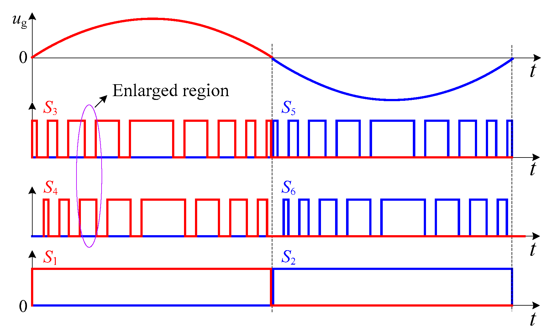
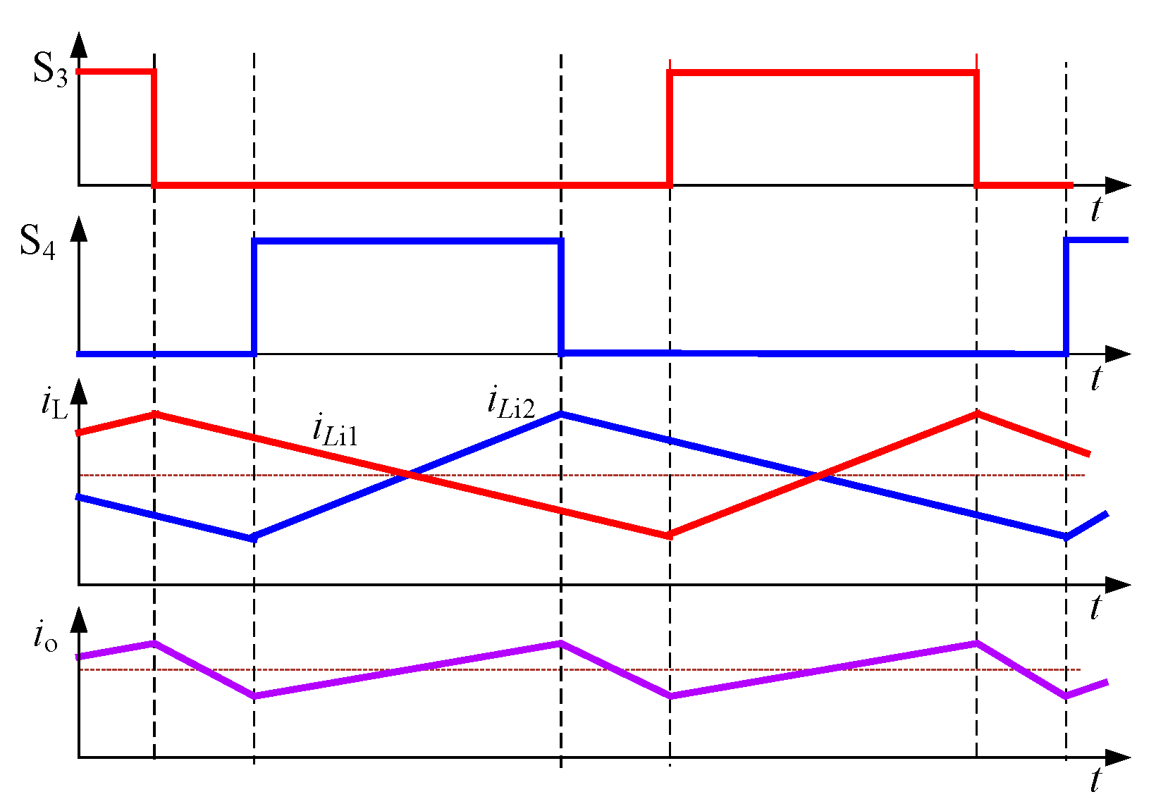
2.2. Operation Principles

In order to simplify the analysis, the following assumptions are proposed:
(1)
All devices in the topology are ideal.
(2)
Compared with the grid current, the current of output capacitor Cf is small enough to be ignored.
(3)
The circuit is in a steady state.
Based on the above assumptions, each state can be divided into four intervals according to the operation of the interleaving unit. The equivalent circuits of the four intervals in the inverter state are shown in Figure 2. The equivalent circuits of the four intervals in the rectifier state are shown in Figure 3.
Inverter interval a: In the positive half period of the grid, the inverter interleaving unit 1 works. S1 is always on and S5, S6, D1, D2, D3, and D4 are disconnected. There is a 180 degree phase difference between the driving signal of S3 and that of S4. S3 and S4 are interleaved turned on, and energy is supplied from the DC side to the AC side through inductors Li1, Li2, and Lg.
Inverter interval b: In the positive half period of the grid, the inverter interleaving unit 1 works. S1 is always on and S5, S6, S3, S4, D3, and D4 are disconnected. D1 and D2 turn-on, and energy in inductors Li1, Li2, and Lg is supplied to the AC side by diodes.
Inverter interval c: In the negative half period of the grid, the inverter interleaving unit 2 works. S2 is always on and S3, S4, D1, D2, D3, and D4 are disconnected. There is a 180 degree phase difference between the driving signal of S5 and that of S6. S5 and S6 are interleaved turned on, and energy is supplied from the DC side to the AC side through inductors Li3, Li4, and Lg.
Inverter interval d: In the negative half period of the grid, the inverter interleaving unit 2 works. S2 is always on and S3, S4, S5, S6, D1, and D2 are disconnected. D3 and D4 turn-on, and energy in inductors Li3, Li4, and Lg is supplied to the AC side by diodes.
Rectifier interval a: In the positive half period of the grid, the rectifier interleaving unit 1 works. S3 and S4 are always on. S1, S2, D1, D2, D3, and D4 are disconnected. There is a 180 degree phase difference between the driving signal of S5 and that of S6. S5 and S6 are interleaved turned on, and AC energy flows through the switch to charge inductors Li1, Li2, Li3, Li4, and Lg, and the energy in the inductors rises.
Rectifier interval b: In the positive half period of the grid, the rectifier interleaving unit 1 works. S3 and S4 are always on and S1, S2, S5, S6, D1, and D2 are disconnected. D3 and D4 turn-on, energy in the inductors and AC energy are superimposed to the DC side, and the energy in the inductances decreases.
Rectifier interval c: In the negative half period of the grid, the rectifier interleaving unit 2 works. S5 and S6 are always on. S1, S2, D1, D2, D3, and D4 are disconnected. There is a 180 degree phase difference between the driving signal of S3 and that of S4. S3 and S4 are interleaved turned on, and AC energy flows through the switch to charge inductors Li1, Li2, Li3, Li4, and Lg, and the energy in the inductors rises.
Rectifier interval d: In the negative half period of the grid, the rectifier interleaving unit 2 works. S5 and S6 are always on and S1, S2, S3, S4, D3, and D4 are disconnected. D1 and D2 turn-on, energy in the inductors and AC energy are superimposed to the DC side, and the energy in the inductances decreases.

2.3. Ripple Analysis
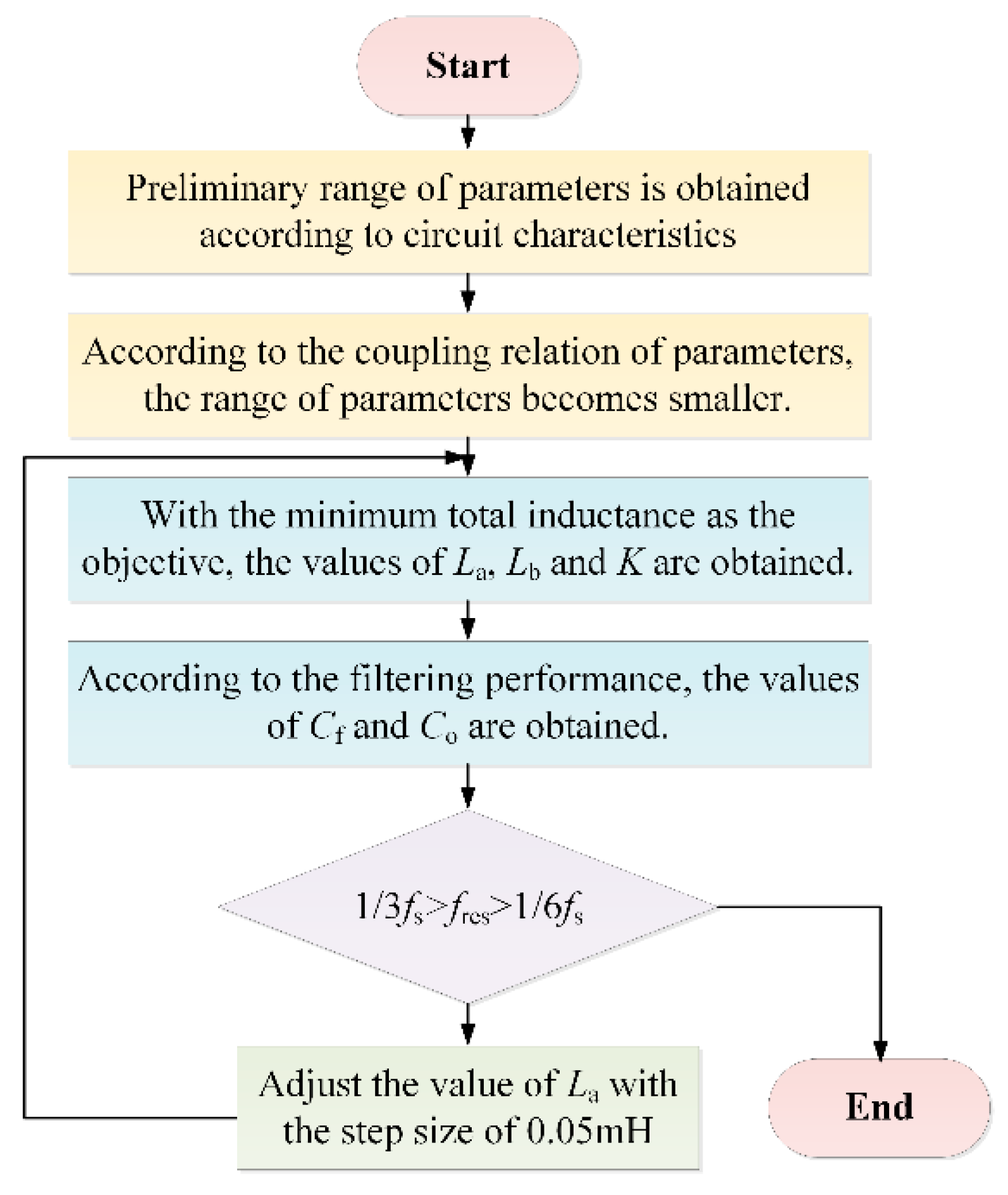
According to the model analysis of the equivalent circuits, the sequence diagram of the inverter state is depicted in Figure 4. In the inverter state, the operation cycle of S1 and S2 is the same as that of the power grid. The operation frequencies of S3, S4, S5, and S6 are all 50 kHz. In the positive half-cycle of the grid, S1 is always on and S3 and S4 are interleaved turned-on. In the negative half-cycle of the grid, S2 is always on and S5 and S6 are interleaved turned-on.
By magnifying the driving waveform region marked by the arrow in Figure 4, the detailed waveforms can be obtained as in Figure 5. Moreover, the current waveforms of inductors Li1 and Li2 are drawn according to the driving waveforms. It is obvious that the sum of the inductance current ripples of the interleaving unit is lower than that of any branch of the interleaving unit. It is proved that interleaved parallel technology can reduce the requirement of inductance and reduce the circuit weight. Further, the sequence diagram analysis of the rectifier state is similar to that of the inverter state. Therefore, the description is not repeated here.

3. Parameter Design

The performance of the filter is directly affected by the filter parameters. Thereby, the parameters of the filter should be designed carefully to obtain the desirable performance. As for the proposed converter, the filter consists of Li1, Li2, Li3, Li4, Lg, Cf, and Co. Among them, Li1, Li2, Li3, Li4, Cf, and Lg constitute the LCL filter in the inverter state, and Li1, Li2, Li3, Li4, Lg, and Co constitute the LC filter in the rectifier state. It is obvious that the structures of the filter are different in the two states. In addition, the coupling relationship among the filter parameters leads to the interaction of parameters. As a consequence, the conventional parameter design method for the unidirectional converter is no longer applicable to the proposed converter.
In this paper, a novel parameter design method is proposed, which takes into account the performance requirements of the two states. The main goal is to fulfill high power density, good filtering performance, and good steady-state performance. The method can be divided into three steps. To start with, a generalized range of filter parameters is obtained according to the working principle and process of the circuit. Secondly, the range of filter parameters is optimized by analyzing the coupling relationship among the parameters. In the end, a set of reasonable parameters is obtained by setting the priority of the filter performance index. The specific design process of this method will be given in detail as follows. In order to simplify the analysis process, it is assumed that the inductance values of Li1, Li2, Li3, and Li4 are equal, which are denoted by Li. Further, the equivalent total inductance La in the inverter state and the total inductance Lb in the rectifier state is defined as shown in (1):
{ L a = L i + L g L b = 1.5 L i + L g

3.1. Parameter Selection

The proposed converter has two states of inverter and rectifier. According to the equivalent circuit and operation mode, the filter parameters of the two states are calculated separately. The preliminary range of filter inductance and capacitance is obtained.

3.1.1. Preliminary Range of Filter Inductance

According to the working principle of the converter, the voltage vector diagram of the converter in different states is drawn as shown in Figure 6. In the figure, grid voltage vector is represented by ug, grid current vector is represented by ig, total filter inductance voltage vector is represented by uL, DC voltage vector is represented by udc, and θ represents the angle between udc and ug. According to the different impedance angles of the power grid, the angle of ig lagging behind ug will change, and at the same time θ will also change.
According to the voltage vector diagram, the relationship among udc, ug, and ig can be obtained from cosine theorem as shown in (2):
u L 2 = u dc 2 + u g 2 2 u dc u g cos θ .
Formula (3) can be obtained by deriving θ from (2):
d u L 2 d θ = 2 u dc u g sin θ .
From (3), we can see that uL is proportional to θ. When the phase of ig and ug is the same, θ is the largest. Therefore, the maximum inductance voltage uL_max is obtained in (4). Where L represents the total inductance in the filter circuit, iL is the filter inductance current and ω is the rated angular frequency of the grid.
{ u L _ max = ω L i L u L _ max 2 = u dc 2 u g 2
The filter inductances of the inverter and rectifier states are calculated respectively. According to (4), the maximum total inductance La_max of the converter in the inverter state can be expressed as (5), where Vdc, Vg represent DC voltage and grid voltage.
L a _ max = L i + L g = V dc 2 V g 2 ω i L
In the inverter state, in order to prevent the converter from producing high current ripple, the converter should work in continuous conduction mode (CCM). The critical inductance value La_min1, which satisfies the CCM in the inverter state, can be obtained by (6). Where d represents duty cycle, idc is direct current, fs is switching frequency, and Vgm is the peak value of the grid voltage.
{ L a _ min 1 = L i + L g = V dc ( 1 d ) d 2 2 i dc f s d = V gm V dc sin ( ω t )
The derivation of d in (6) shows that the critical inductance value is the largest when d is 2/3 in the inverter state. The duty cycle d varies sinusoidally with time in the inverter state. Therefore, in order to ensure that the converter always works in CCM, the equivalent filter inductance should be larger than the maximum critical inductance La_min1.
According to the working principle of the Buck circuit, the ripple ΔIa of the inductance current in the inverter state is calculated as (7), where Ts represents the switching period.
{ Δ I a = V g ( 1 2 d ) T s L a ( d < 0.5 ) Δ I a = ( V dc V g ) ( 2 d 1 ) T s L a ( d > 0.5 ) d = V gm V dc sin ( ω t )
By deriving d from (7), we can see that during d < 0.5, the maximum inductance current ripple ΔIa_max1 can be obtained when d equals 0.25. During d > 0.5, the maximum inductance current ripple ΔIa_max2 can be obtained when d equals 0.75. The value of ΔIa_max1 is equal to Ia_max2, which is VdcTs/8La and can be expressed by ΔIa_max. The minimum equivalent filter inductance La_min2 in the inverter state can be obtained as follows:
L a _ min 2 = L i + L g = V dc T s 8 Δ I a _ max
For the same reason, according to (4), the maximum total inductance Lb_max of the converter in the rectifier state can be obtained:
L b _ max = 1.5 L i + L g = V dc 2 u g 2 ω i L
Similarly, in order to prevent the converter from producing high current ripple in the rectifier state, the converter should work in CCM. The critical inductance value Lb_min1, which satisfies the CCM in the rectifier state, can be obtained by (10).
{ L b _ min 1 = 1.5 L i + L g = V dc ( 1 d ) 2 d 2 i dc f s d = V dc V gm sin ( ω t ) V dc
The derivation of d in (10) shows that the critical inductance value is largest when d is 1/3 in the rectifier state. The duty cycle d varies with time in the rectifier state. Therefore, in order to ensure that the converter always works in CCM, the equivalent filter inductance should be larger than the maximum critical inductance Lb_min1.
According to the working principle of the Boost circuit, the ripple ΔIb of the inductance current in the rectifier state is calculated as (11).
{ Δ I b = ( V dc V g ) ( 1 2 d ) T s L b ( d < 0.5 ) Δ I b = V g ( 2 d 1 ) T s L b ( d > 0.5 ) d = V dc V gm sin ( ω t ) V dc
By deriving d from (11), we can see that during d < 0.5, the maximum inductance current ripple ΔIb_max1 can be obtained when d equals 0.25. During d > 0.5, the maximum inductance current ripple ΔIb_max2 can be obtained when d equals 0.75. The value of ΔIb_max1 is equal to Ib_max2, which is VdcTs/8Lb and can be expressed by ΔIb_max. The minimum equivalent filter inductance Lb_min2 in the rectifier state can be obtained as follows:
L b _ min 2 = 1.5 L i + L g = V dc T s 8 Δ I b _ max .

3.1.2. Preliminary Range of Filter Capacitance

When the converter operates in the inverter state, to ensure high power factor to transfer energy based on the converter hardware, according to the standard IEEE-519/IEEE-1547, the output reactive power must not exceed 5% of the active power. Thus, the maximum value Cfmax of the filter capacitor can be obtained as shown in (13). Where Sn is the rated capacity of the converter, Un is the rated voltage of the grid.
C fmax = S n ω U n 2 5 %
When the converter operates in the rectifier state, to ensure that the output voltage meets the ripple requirement, according to the standard GB/T3797-1989, the fluctuation of the DC voltage could not exceed 15% of the rated voltage value. Thus, the minimum value of the filter capacitor is Co_min, as shown in (14). Where Po represents the output power of the converter, Vn is the rated voltage of the DC bus, and ΔV is the voltage ripple of the DC bus.
C o _ min = P o 2 π f s V n Δ V

3.2. Parameter Optimization

Since during the rectifier state, the filter was equal to a second-order system, there was no coupling relationship between the inductance parameters of the filter. Therefore, this section only focuses on the inverter state. In the inverter state, grid-connected current harmonics mainly include two aspects: (1) High-order harmonics generated by switching operation; (2) Low-order harmonics introduced under the background of the power grid. Among them, the frequency of the low-order harmonics is lower than the shear frequency of the closed loop system. Therefore, low-order harmonics can be suppressed by control [22], while high-order harmonics are difficult to suppress. In order to improve the waveform quality, it is necessary to design the filter reasonably to suppress the high-order harmonic current. Next, according to the suppression ability of the high-order harmonic current, the relationship among the filter parameters in the inverter state is decoupled. The range of the filter parameters is optimized.
From Figure 1, the transfer function between input voltage Vdc and harmonic current if can be obtained as shown in (15). Where ωf represents the angular switching frequency, K is the ratio of Li to Lg. Let Vdc be 1, draw three-dimensional curves of if, K, and Cf under different La values as shown in Figure 7. It can be seen that with the increase of the equivalent filter inductor La, the attenuation ability of the filter to harmonic current if increases gradually.
G i f _ V bus ( s ) = i f V dc = Z c ( ( Z g Z c ) + ( ( Z g + Z c ) Z i ) ) = 1 ω f ( ω f 2 L i L g C f + L i + L g ) = 1 ω f ( ω f 2 L a 2 ( K 1 + K ) ( 1 1 + K ) C f + L a )

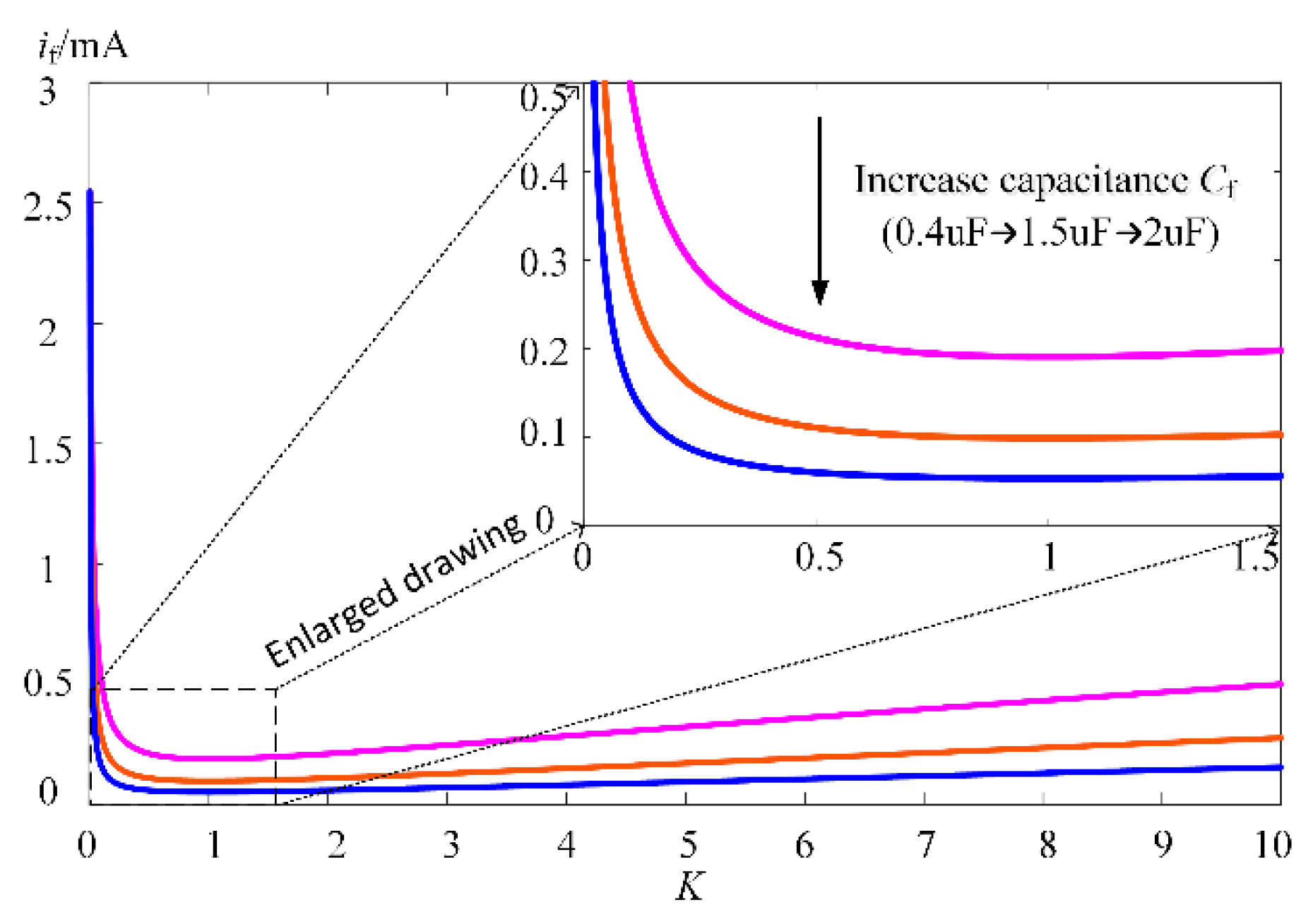
3.2.1. Range Optimization of Inductance Ratio

When La is constant, the relationship between if and K is shown in Figure 8. When K changes from 0 to 1, the attenuation ability of the filter to harmonic current increases gradually and if decreases rapidly. When K = 1, the filter has the strongest attenuation ability to the harmonic current, and if is lowest. As K continues to increase, the attenuation ability of the filter to harmonic current decreases, and if increases slowly. However, too small K will result in too large Lg and too large an inductance core. Therefore, considering the size and filtering effect of the filter, K usually takes about 3–7.

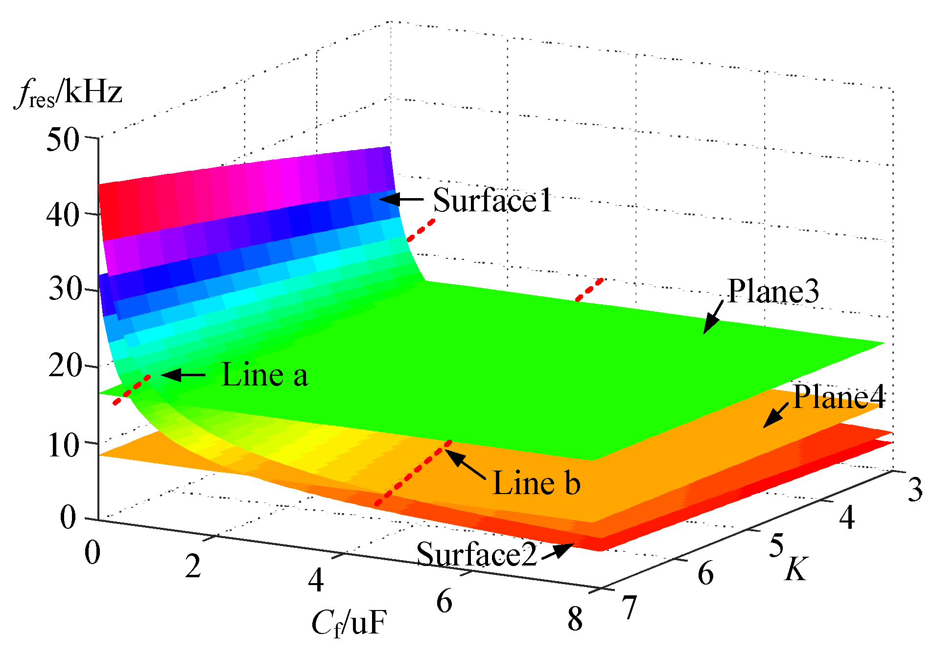
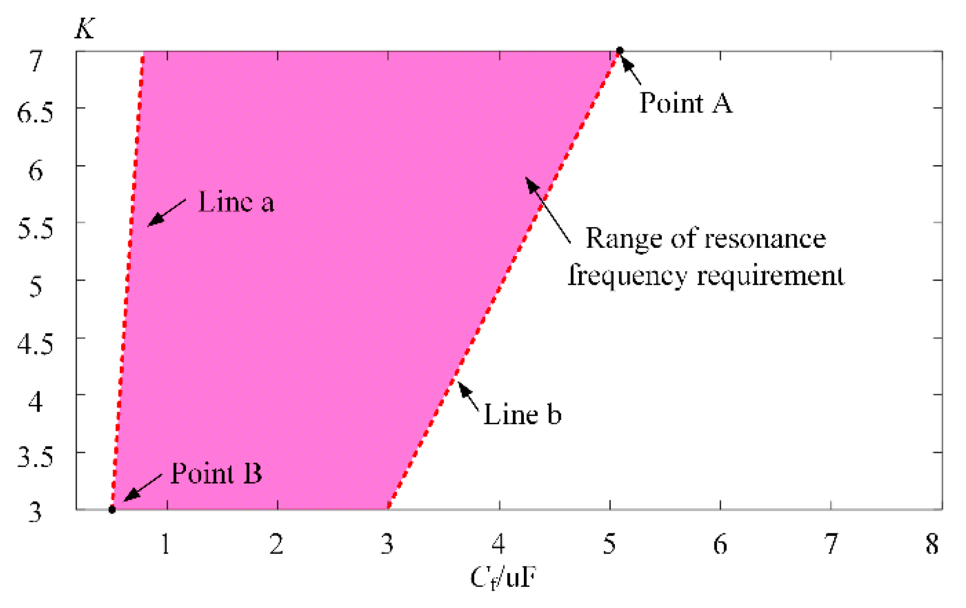
3.2.2. Range Optimization of Capacitance

Similarly, when La is constant, the relationship between if and Cf is shown in Figure 9. As the value of Cf increases from 0, if decreases greatly. When Cf increases to 2.5 uF, the attenuation curve of the filter to the harmonic current tends to be flat. On this basis, Cf-z is defined as the critical filter capacitor to reduce if to 20% of the maximum harmonic current. Therefore, in order to make a filter with a high attenuation performance, the value of Cf should be greater than Cf-z.

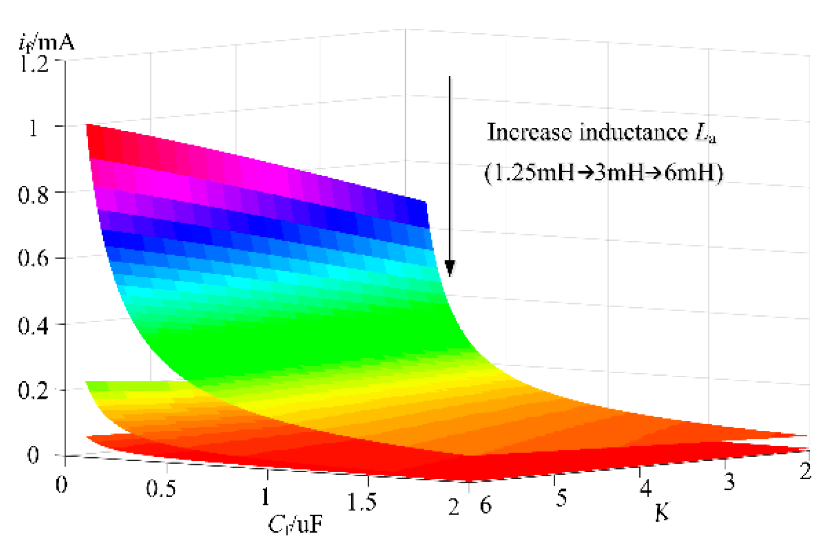
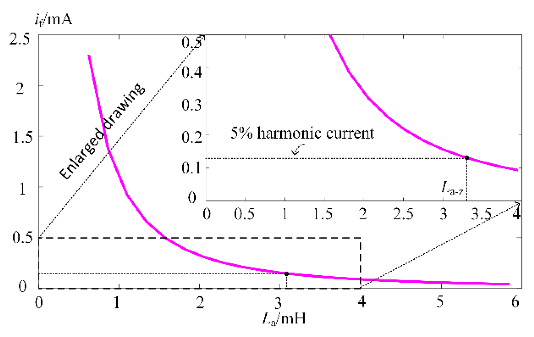
3.2.3. Range Optimization of Inductance

According to the above analysis, when K chooses the maximum value and Cf chooses the minimum value, the filter has the weakest ability to suppress harmonic current. Under this limit condition, the relationship between if and La is plotted as shown in Figure 10. With the increase of La, the suppression ability of the filter to the harmonic current is gradually enhanced. On this basis, LZ is defined as the critical filter inductance to reduce if to 5% of the maximum harmonic current. When La reaches Lz, the filter has a strong suppression ability to the harmonic current and the suppression curve tends to be flat. Therefore, in order to reduce the volume and cost of the converter, the critical inductance Lz can be used as the maximum value of La.

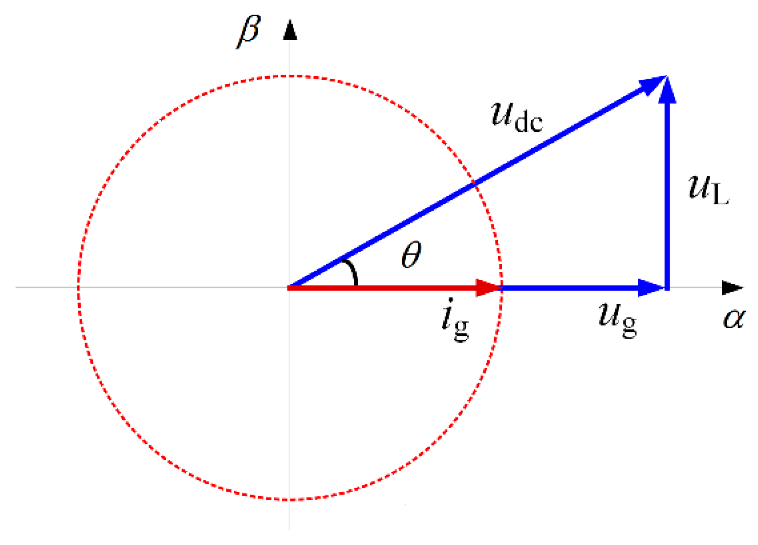
3.3. Stability Analysis

In order to make the system run stably, the stability of the two states was analyzed. According to the stability condition, the filter parameters are further optimized.

3.3.1. Stability in the Inverter State

The filter of the converter is a third-order system in the inverter state and it is easy to lose stability during operation. To realize the smooth operation of the system, the resonant frequency fres of the third-order filter should be between 1/6 and 1/3 of the switching frequency [23,24,25]. In this paper, the switching frequency is 50 kHz, so the resonant frequency of the filter ranges from 8.3 kHz to 16.6 kHz. The resonant frequency of the converter in the inverter state can be obtained by (16).
f r e s = 1 2 π L i + L g L i L g C f = 1 2 π ( 1 + K ) 2 K L a C f
From the analysis of (16), it can be seen that fres is inversely proportional to La, as fres decreases with the increase of La. Therefore, by substituting the obtained limit value of La into (16), the three-dimensional surface of K, Cf, and fres is obtained as shown in Figure 11. Surface 1 is the surface obtained by substituting the minimum value of La, and surface 2 is the surface obtained by substituting the maximum value of La. Plane 3 is a horizontal plane with a resonant frequency of 16.6 kHz. Plane 4 is a horizontal plane with a resonant frequency of 8.5 kHz.
As can be seen in Figure 11, when La is the maximum value, the minimum value of Cf satisfying the resonant frequency requirement can be obtained. Similarly, when La is the minimum value, the maximum value of Cf satisfying the resonant frequency requirement can be obtained. Therefore, the intersection line a of surface 2 and plane 3 and the intersection line b of surface 1 and plane 4 in Figure 11 can be projected on the X-Y plane to obtain Figure 12. From Figure 12, the maximum value of Cf is at point A, which corresponds to a value of 5.1 uF. The minimum value of Cf is at point B, which corresponds to a value of 0.4 uF. A smaller range of Cf can be obtained as shown in (17).
0.4   u F C f 5.1   u F
Similarly, from Figure 12, it can be seen that K can meet the requirements of resonant frequency fres in the range of 3–7, so the range of K is still 3–7.

3.3.2. Stability in the Rectifier State

The filter of the converter is a second-order system in the rectifier state. The transfer function between the output voltage Uo and the input voltage Uin is shown in (18). In order to ensure the stability of the system, the damping ratio ξ of the second-order filter should be between 0 and 1, so that the system can work in an under-damped state.
G ( s ) = U o ( s ) U in ( s ) = 1 L b C o s 2 + L b R s + 1
where ξ can be expressed as (19). R is the 10% overload value of the converter in the rectifier state.
ξ = L b C o / ( 2 R C o )
The Co_min of (14) is substituted into (19), and the maximum value of Lb can be obtained according to the range value of ξ.

3.4. Performance Index

In order for the converter to have better performance, power density, filtering performance, and stability are taken as optimization targets. The relationship between filter parameters and performance indexes in the two states is analyzed. The results show that the relationships among the performance indexes are constrained by each other. Therefore, priority setting is adopted to take into account multiple optimization targets.

3.4.1. Power Density Performance Index

According to the topology of the converter in Figure 1, the total inductance Lall of the converter is defined as the sum of all inductance values, which can be obtained by (20).
{ L all = 4 L i + L g L i = L i 1 = L i 2 = L i 3 = L i 4
In the inverter state, the equivalent filter inductor La:
L a = L i + L g .
Substitute (21) into (20) to obtain:
L all L a = 4 K + 1 K + 1 .
In the rectifier state, the equivalent filter inductor Lb:
L b = 1.5 L i + L g .
Substitute (23) into (20) to obtain:
L all L b = 6 K + 1 1.5 K + 1 .
Combining equations (22) and (24), Lall is proportional to K in both states. Therefore, to get the minimum inductance value, K should choose the minimum value to achieve the high power density performance.

3.4.2. Filtering Performance Index

In the inverter state, the filtering performance is expressed by γ, which is the ratio of the post-filter harmonic current ih_o to the pre-filter harmonic current ih_i. Using the two-port principle, γ can be obtained as:
γ = i h _ o i h _ i = Z 21 Z 22 = Z 2 Z 2 + Z 3 = 1 1 + w f 2 C f L g .
Formula (25) shows that the attenuation γ of the filter is inversely proportional to Cf and Lg. Therefore, to achieve the best filtering effect and minimum attenuation γ, Cf, and Lg should be maximized. Where the value of Lg is determined by La and K, Lg can be obtained by (26).
L g = L a 1 1 + K
According to (26), Lg is proportional to La and inversely proportional to K. That is to say that the filtering performance index is proportional to La and inversely proportional to K.
In the rectifier state, the filtering performance is expressed by h, which is the ratio of the post-filter harmonic voltage uh_o to the pre-filter harmonic voltage uh_i. Using the circuit principle, h can be obtained as (27), where ωh represents the harmonic voltage angle frequency.
h = u h _ o u h _ i = 1 L b C o ω h 2 + ω h L b R + 1
Formula (27) shows that the harmonic voltage ratio h is inversely proportional to Co and Lb. Therefore, to achieve the best filtering effect and the minimum harmonic voltage ratio h, Co, and Lb should be maximized.

3.4.3. Stability Performance Index

In the inverter state, to ensure the stable operation of the system, the resonant frequency of the filter should be between 1/6fs and 1/3fs. However, the value of the filter inductance will decrease with the increase of power, which will easily cause resonance frequency offset and affect the stability. Therefore, considering the variation of the filter inductance, the resonant frequency can be obtained from (28), where ɑ represents the ratio of the changed inductance to the initial inductance, which is always less than 1.
f r e s = 1 2 π α L i + α L g α L i α L g C f = 1 2 π ( 1 + K ) 2 K α L a C f
As can be seen from (28), fres is inversely proportional to La and Cf, and directly proportional to K.
In the rectifier state, to ensure the stable operation of the system, the damping ratio ξ should be between 0 and 1. Similarly, the value of the filter inductance varies with the increase of power. Therefore, considering the variation of the filter inductance, the damping ratio can be obtained by (29).
ξ = α L b C o / ( 2 R C o ) = α L b C o / ( 2 R C o )
By substituting the obtained range of filter parameters into (29), it can be seen that the damping ξ ratio is less than 1. Therefore, the parameters in this range can satisfy the stability of the system. Therefore, the stability under the rectifier state is not discussed in the later analysis.

3.4.4. Performance Index Priority

According to the previous analysis, the relationship between filter parameters and performance indexes can be known. Among them, the total inductance of the filter is proportional to La, Lb, and K. The filtering performance is proportional to Cf, Co, La, and Lb, and is inversely proportional to K. The stability of the filter (i.e., the resonant frequency of the filter) is inversely proportional to La and Cf, and is proportional to K. The specific relationship is shown in Table 1 below.
As can be seen in Table 1, we can see that the relationship between the three performance indexes and the filter parameters is contradictory. Therefore, the three performance indexes cannot be optimized at the same time. To solve this problem, priority setting is adopted to take into account multiple optimization targets. The specific methods are as follows: (1) The power density index is taken as the first priority, and the minimum total inductance is taken as the target. The values of the equivalent filter inductor La, Lb, and inductance ratio K are obtained. (2) Taking the filtering performance index as the second priority, the preset attenuation γ is less than 0.08 and harmonic voltage ratio h is less than 0.1. The value of filter capacitance Cf and Co are obtained. (3) The stability index is used as the verification condition to judge whether the obtained filter parameters are reasonable or not. If not, the value of La can be adjusted by 0.05 mH step size, and the adjusted La value can be recalculated into the filter performance index to obtain new parameter values until the parameters are reasonable. The filter parameters are optimized through the above steps, and the flow chart of the parameter design is shown in Figure 13. The specific filter parameters are obtained as shown in Table 2. So far, the parameter design process of the filter is completed.

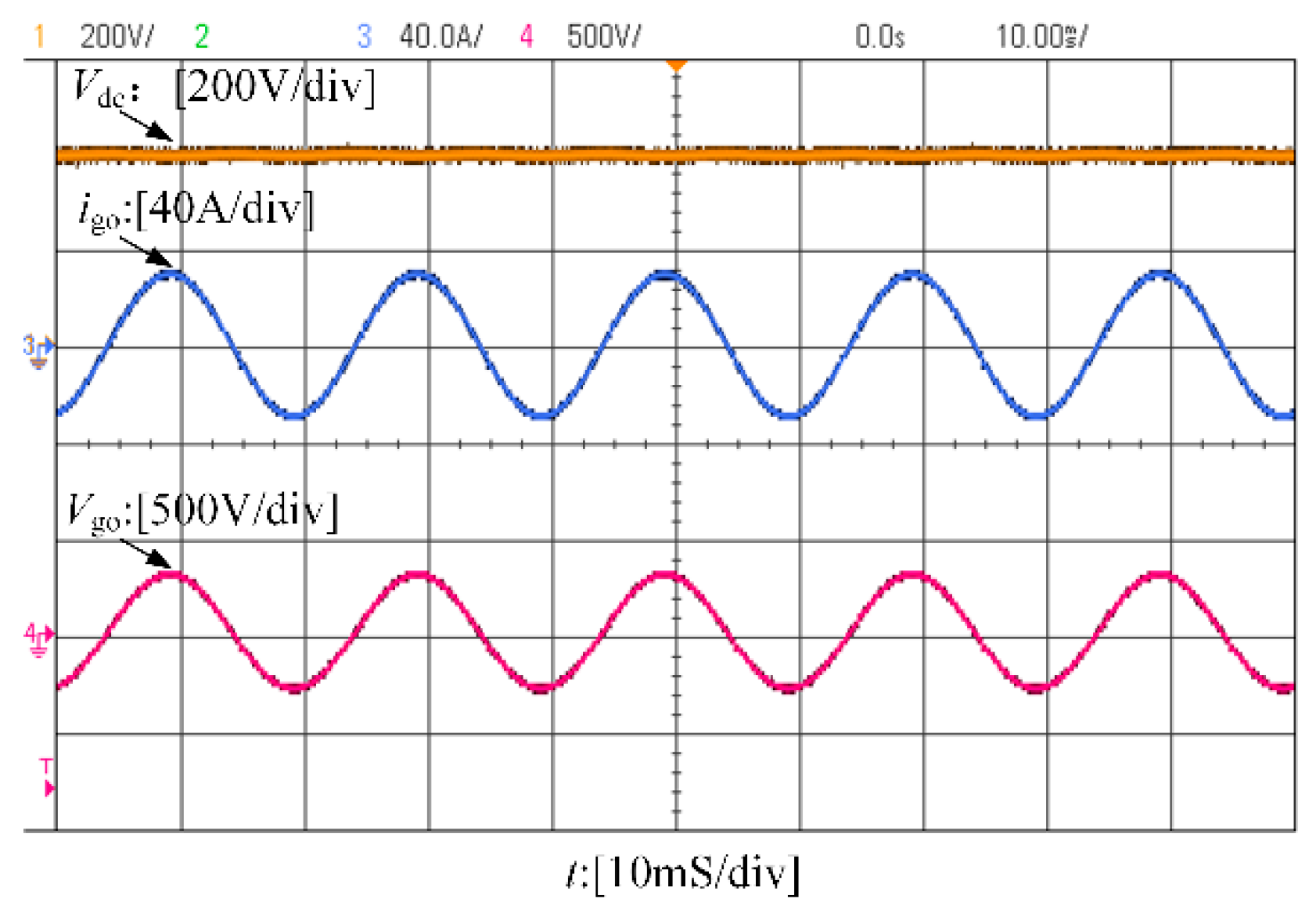
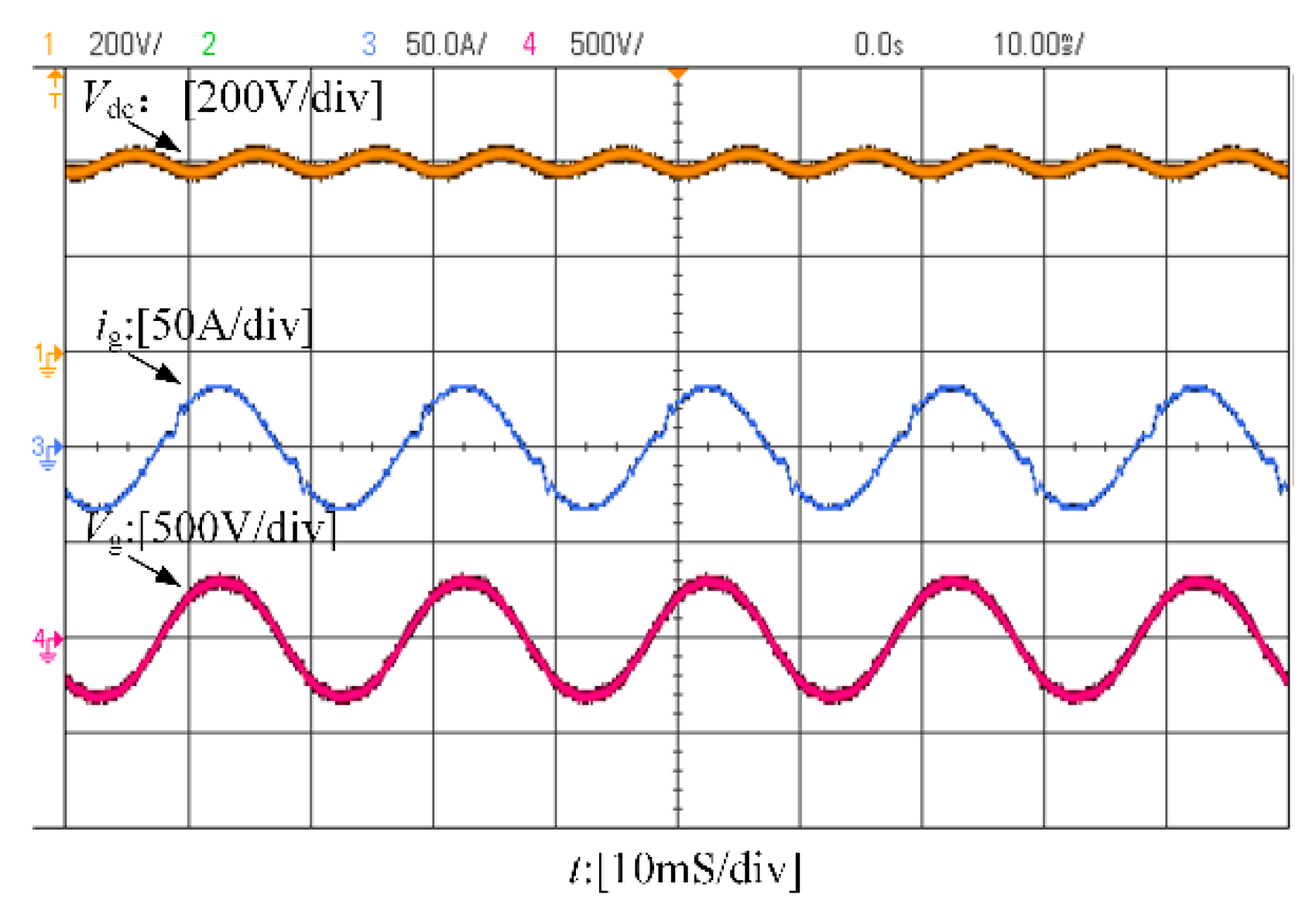
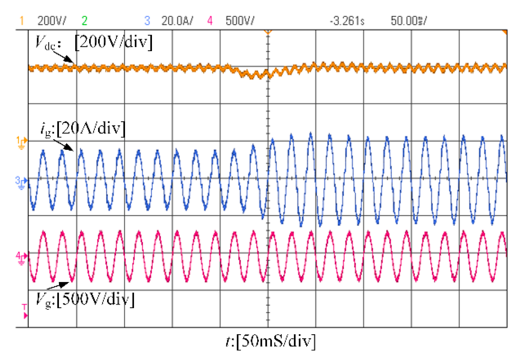
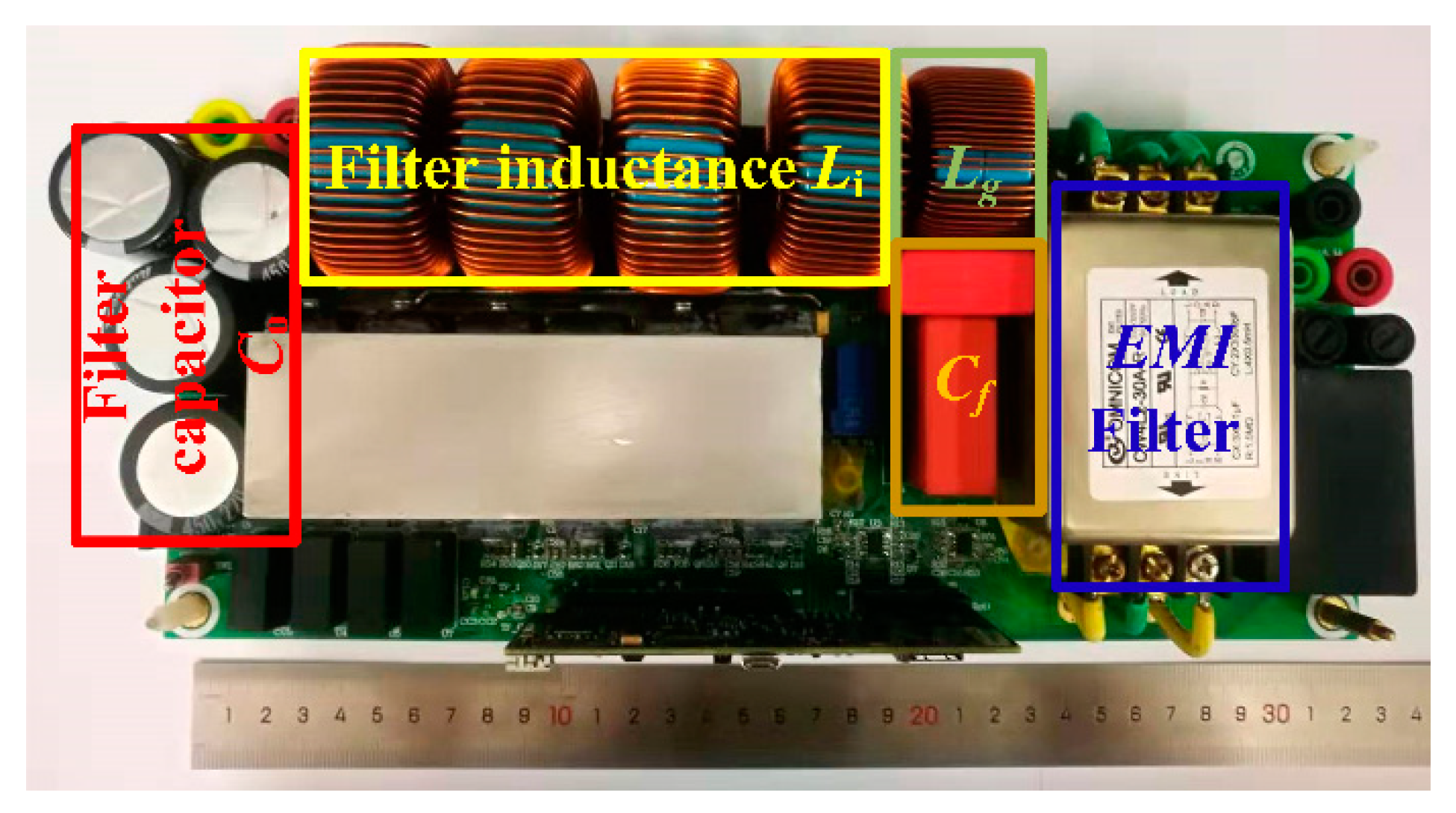
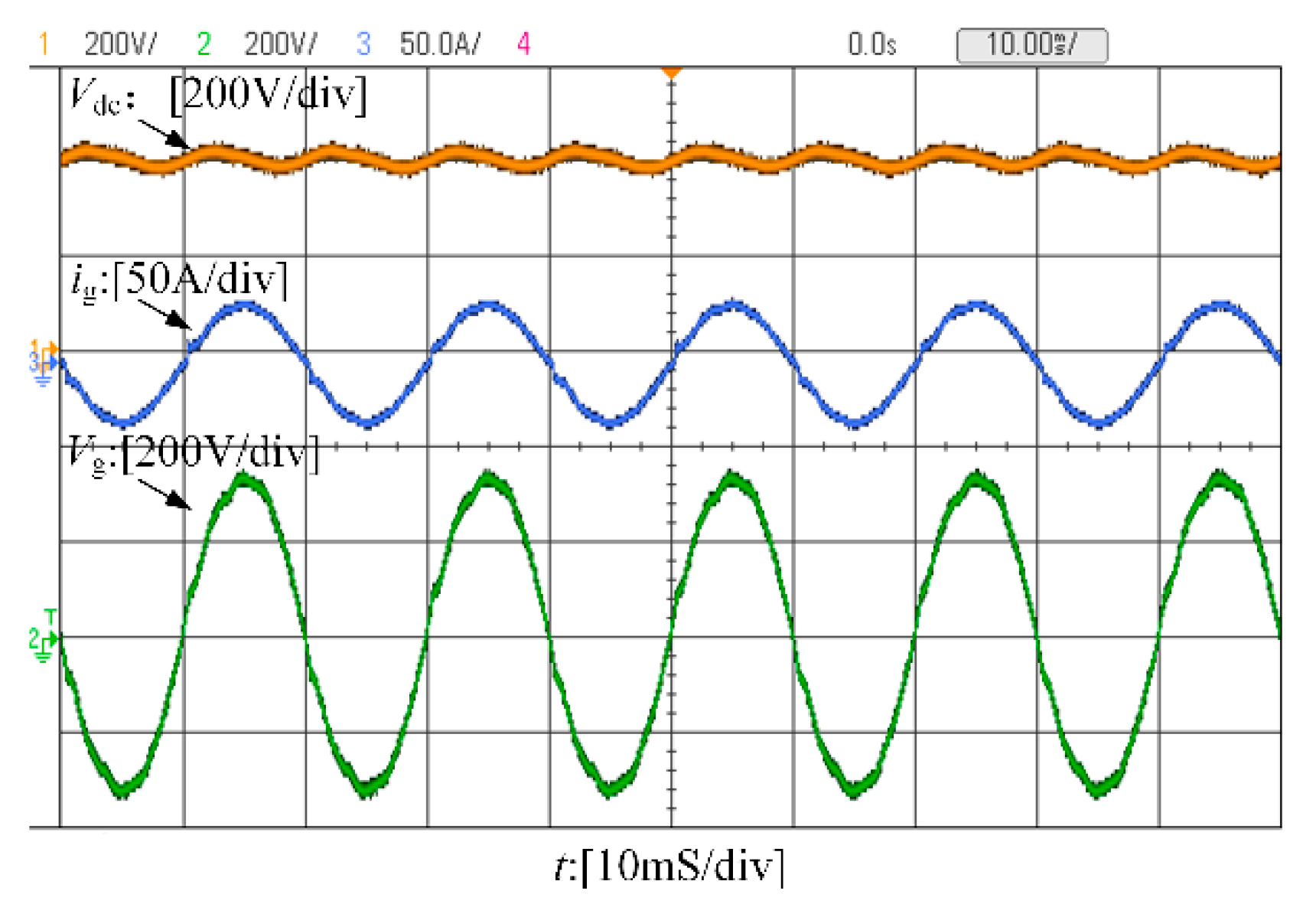
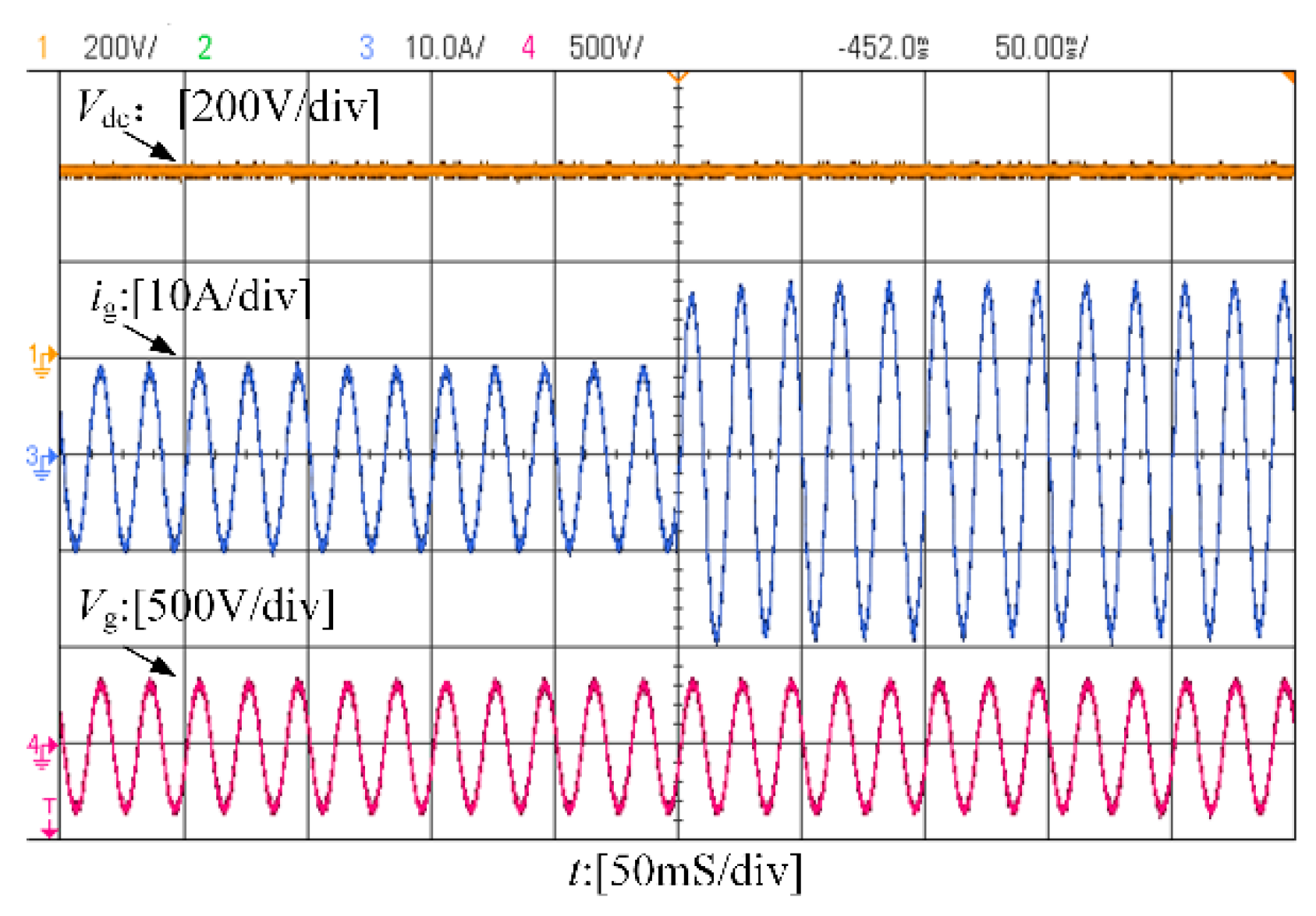
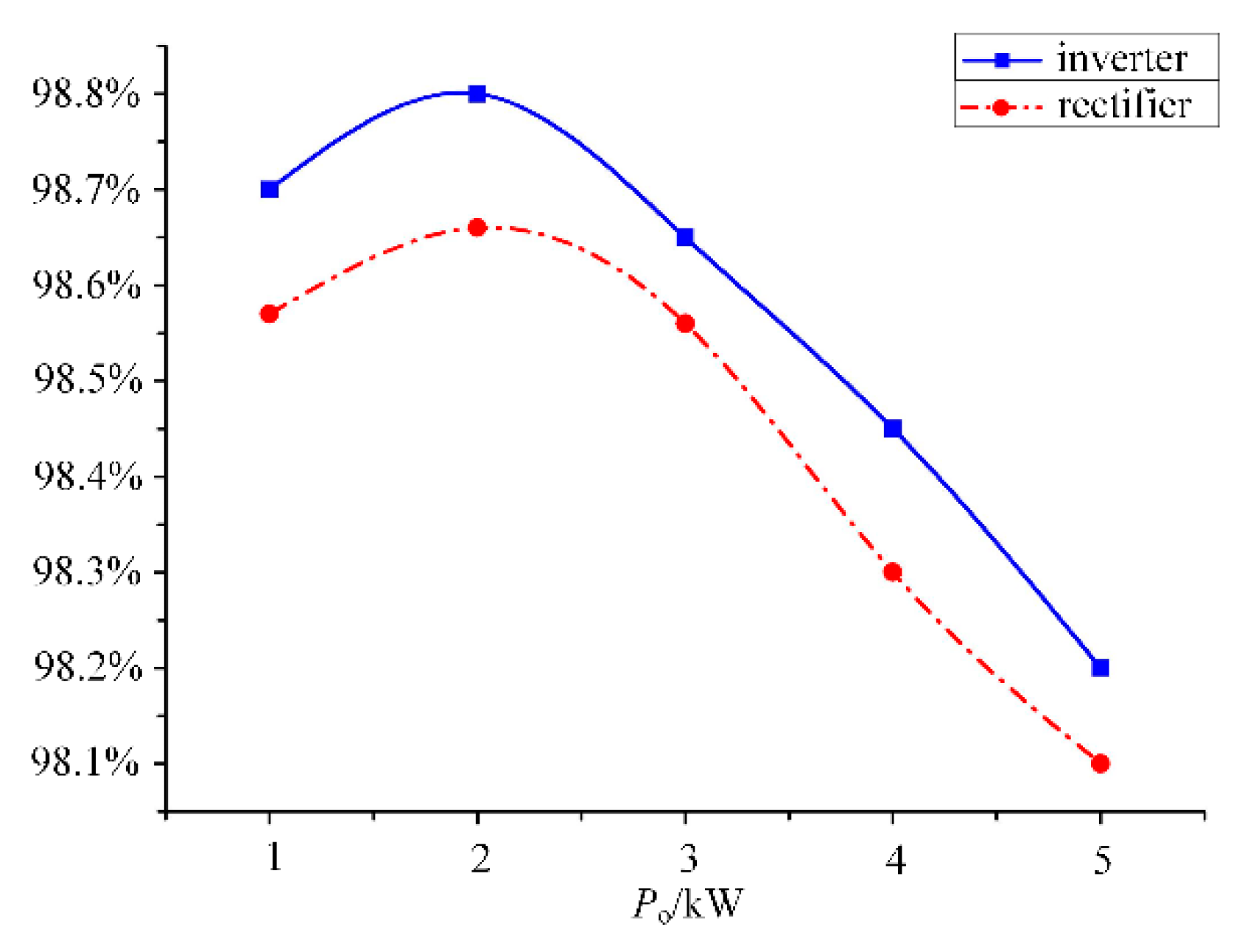
4. Experimental Result

In order to verify the validity of the parameter design method for the proposed converter, a prototype with a rated power of 5 kW was built, as shown in Figure 14, with a power density that reached 36 W/in3. The processor chip used was 28377D (Texas Instruments, Dallas, TX, USA), and the experiments were carried out under two states of inverter and rectifier, respectively.
Figure 15 shows the experimental waveforms of the converter under full load in the grid-connected inverter state. Where Vdc denotes DC voltage, Vg denotes grid voltage, and ig denotes grid current. In the figure, the phases of ig and Vg are the same, and the waveform ig has good sinusoidal degree and small distortion. Further, when the number of harmonics is calculated to be 15 times, the THD of ig is only about 2.7%.
Figure 16 shows the experimental waveforms of the converter under full load in the off-grid inverter state. Where igo denotes output current, Vgo denotes output voltage. In the figure, the waveforms igo, Vgo have good sinusoidal degree and small distortion. Further, when the number of harmonics is calculated to be 15 times, the THD of ig is only about 1.2%.
Figure 17 shows the experimental waveforms of the converter under full load in the rectifier state. In the figure, the phase of ig and Vg is the same. The fluctuation of the DC bus voltage is less than 15% of the rated voltage of 400 V, which meets the design requirements. Further, when the number of harmonics is calculated to be 15 times, the THD of ig is 4.5%.
Figure 18 shows the dynamic experimental waveforms of the converter under the inverter grid-connected state. In the figure, the dynamic recovery time of the converter is shorter and the converter has better stability.
Figure 19 shows the dynamic experimental waveforms of the converter in the rectifier state. In the figure, it can be seen that the change of the Vdc before and after the power dynamic conversion is small and the dynamic recovery time of the converter is shorter. The results show that the converter has high stability.
In summary, the efficiency curves in the two states are shown in Figure 20. From the figure, the maximum efficiencies of the grid-connected inverter and rectifier are 98.8% and 98.66%, respectively. The efficiencies of the grid-connected inverter and rectifier under full load are 98.2% and 98.1%, respectively.

5. Conclusions

This paper proposes an interleaved, dual-buck, bidirectional, grid-connected converter topology and related filter parameters optimization design method. This method has several optimization design goals, including filter inductance, filtering performance, and system stability. For one thing, the performance requirements of the filter in the inverter and rectifier states are simultaneously considered. For another, the total inductance of the converter is small enough and the steady-state performance is good. The specific design process is as follows: (1) The coupling relationship between circuit performance and filter parameters is considered, and the parameter range of the filter is continuously reduced. (2) Set the performance priority of the filter and optimize the reasonable value of the filter parameters. Thereby, beneficial properties such as higher power density, better filtering effect, and higher steady-state stability are obtained. Finally, a 5 kW experimental prototype was used to prove the validity of the theoretical analysis. Its power density was 36 W/in3. Under full load conditions, the THDs of grid currents in among grid-connected inverter, off-connected inverter, and rectifier states are 2.7%, 1.2%, and 4.5%, respectively with 0.5 mH buck inductance. The maximum efficiencies of the converter are 98.8% and 98.66% in the grid-connected inverter state and the rectifier state, respectively.

Author Contributions

Conceptualization, Y.C.; Formal analysis, Y.C.; Resources, Y.W.; Software, X.M.

Funding

This research was funded by the National Key R&D Program of China (Grant: 2018YFB0904700).

Conflicts of Interest

The authors declare no conflict of interest.

References

  1. Zhang, C.; Jiang, D.; Zhang, X.; Chen, J.; Ruan, C.; Liang, Y. The Study of a Battery Energy Storage System Based on the Hexagonal Modular Multilevel Direct AC/AC Converter (Hexverter). IEEE Access 2018, 6, 43343–43355. [Google Scholar] [CrossRef]
  2. Vavilapalli, S.; Subramaniam, U.; Padmanaban, S.; Ramachandaramurthy, V.K. Design and Real-Time Simulation of an AC Voltage Regulator Based Battery Charger for Large-Scale PV-Grid Energy Storage Systems. IEEE Access 2017, 5, 25158–25170. [Google Scholar] [CrossRef]
  3. Li, R.; Wang, W.; Xia, M. Cooperative Planning of Active Distribution System With Renewable Energy Sources and Energy Storage Systems. IEEE Access 2018, 6, 5916–5926. [Google Scholar] [CrossRef]
  4. Liu, Y.; Su, M.; Liu, F.; Zheng, M.; Liang, X.; Xu, G.; Sun, Y. Single-Phase Inverter With Wide Input Voltage and Power Decoupling Capability. IEEE Access 2019, 7, 16870–16879. [Google Scholar] [CrossRef]
  5. Ohnuma, Y.; Orikawa, K.; Itoh, J. A Single-Phase Current-Source PV Inverter With Power Decoupling Capability Using an Active Buffer. IEEE Trans. Ind. Appl. 2015, 51, 531–538. [Google Scholar] [CrossRef]
  6. Xu, S.; Shao, R.; Chang, L. Single-phase voltage source inverter with voltage-boosting and power decoupling capabilities. In Proceedings of the IEEE 8th International Symposium on Power Electronics for Distributed Generation Systems, Florianopolis, Brazil, 17–20 April 2017. [Google Scholar]
  7. Chen, C.; Chen, Y.; Tan, Y.; Fang, J.; Luo, F.; Kang, Y. On the Practical Design of a High Power Density SiC Single-Phase Uninterrupted Power Supply System. IEEE Trans. Ind. Inf. 2017, 13, 2704–2716. [Google Scholar] [CrossRef]
  8. Ahsanuzzaman, S.M.; Prodić, A.; Johns, D.A. An Integrated High-Density Power Management Solution for Portable Applications Based on a Multioutput Switched-Capacitor Circuit. IEEE Trans. Power Electron. 2016, 31, 4305–4323. [Google Scholar] [CrossRef]
  9. Gambhir, A.; Mishra, S.K.; Joshi, A. Power Frequency Harmonic Reduction and its Redistribution for Improved Filter Design in Current-Fed Switched Inverter. IEEE Trans. Ind. Electron. 2019, 66, 4319–4333. [Google Scholar] [CrossRef]
  10. Wang, R.; Wang, F.; Boroyevich, D.; Burgos, R.; Lai, R.; Ning, P.; Rajashekara, K. A High Power Density Single-Phase PWM Rectifier With Active Ripple Energy Storage. IEEE Trans. Power Electron. 2011, 26, 1430–1443. [Google Scholar] [CrossRef]
  11. Nguyen, T.-T.; Cha, H.; Nguyen, B.L.-H.; Kim, H.-G. Novel T-type Dual-Buck Inverter with Minimum Number of Inductors. In Proceedings of the 2018 International Power Electronics Conference (IPEC 2018), Niigata, Japan, 20–24 May 2018; pp. 1046–1050. [Google Scholar]
  12. Hong, F.; Liu, J.; Ji, B.; Zhou, Y.; Wang, J.; Wang, C. Single Inductor Dual Buck Full-Bridge Inverter. IEEE Trans. Ind. Electron. 2015, 62, 4869–4877. [Google Scholar] [CrossRef]
  13. Yang, F.; Ge, H.; Yang, J.; Dang, R.; Wu, H. A Family of Dual-Buck Inverters With an Extended Low-Voltage DC-Input Port for Efficiency Improvement Based on Dual-Input Pulsating Voltage-Source Cells. IEEE Trans. Power Electron. 2018, 33, 3115–3128. [Google Scholar] [CrossRef]
  14. Nguyen, B.L.-H.; Cha, H.; Kim, H. Single-Phase Six-Switch Dual-Output Inverter Using Dual-Buck Structure. IEEE Trans. Power Electron. 2018, 33, 7894–7903. [Google Scholar] [CrossRef]
  15. Hong, F.; Liu, J.; Ji, B.; Zhou, Y.; Wang, J.; Wang, C. Interleaved Dual Buck Full-Bridge Three-Level Inverter. IEEE Trans. Power Electron. 2016, 31, 964–974. [Google Scholar] [CrossRef]
  16. Khan, A.A.; Cha, H. Dual-Buck-Structured High-Reliability and High-Efficiency Single-Stage Buck–Boost Inverters. IEEE Trans. Ind. Electron. 2018, 65, 3176–3187. [Google Scholar] [CrossRef]
  17. Meng, Z.; Wang, Y.-F.; Yang, L.; Li, W. High Frequency Dual-Buck Full-Bridge Inverter Utilizing a Dual-Core MCU and Parallel Algorithm for Renewable Energy Applications. Energies 2017, 10, 402. [Google Scholar] [CrossRef]
  18. Jiao, Y.; Lee, F.C. LCL Filter Design and Inductor Current Ripple Analysis for a Three-Level NPC Grid Interface Converter. IEEE Trans. Power Electron. 2015, 30, 4659–4668. [Google Scholar] [CrossRef]
  19. Zheng, X.; Xiao, L.; Lei, Y.; Wang, Z. Optimisation of LCL filter based on closed-loop total harmonic distortion calculation model of the grid-connected inverter. IEEE Trans. Power Electron. 2015, 8, 860–868. [Google Scholar] [CrossRef]
  20. Wu, T.F.; Misra, M.; Lin, L.C.; Hsu, C.W. An Improved Resonant Frequency Based Systematic LCL Filter Design Method for Grid-Connected Inverter. IEEE Trans. Ind. Electron. 2017, 64, 6412–6421. [Google Scholar] [CrossRef]
  21. Liu, Q.; Peng, L.; Kang, Y.; Tang, S.; Wu, D.; Qi, Y. A Novel Design and Optimization Method of an LCL Filter for a Shunt Active Power Filter. IEEE Trans. Ind. Electron. 2014, 61, 4000–4010. [Google Scholar] [CrossRef]
  22. Franklin, G.F. Feedback Control of Dynamic Systems, 2nd ed.; Addison-Wesley Longman: Boston, MA, USA, 1993. [Google Scholar]
  23. Zhou, L.; Zhou, X.; Chen, Y.; Lv, Z.; He, Z.; Wu, W.; Yang, L.; Yan, K.; Luo, A.; Guerrero, J.M. Inverter-Current-Feedback Resonance-Suppression Method for LCL-Type DG System to Reduce Resonance-Frequency Offset and Grid-Inductance Effect. IEEE Trans. Ind. Electron. 2018, 65, 7036–7048. [Google Scholar] [CrossRef]
  24. Wang, J.; Yan, J.D.; Jiang, L.; Zou, J. Delay-Dependent Stability of Single-Loop Controlled Grid-Connected Inverters with LCL Filters. IEEE Trans. Power Electron. 2016, 31, 743–757. [Google Scholar] [CrossRef]
  25. Parker, S.G.; McGrath, B.P.; Holmes, D.G. Regions of Active Damping Control for LCL Filters. IEEE Trans. Ind. Appl. 2014, 50, 424–432. [Google Scholar]
Figure 1. Topological diagram of the proposed converter.
Electronics 08 00973 g001
Figure 2. Equivalent circuits of the inverter state. (a) Inverter a, (b) Inverter b, (c) Inverter c, (d) Inverter d.
Electronics 08 00973 g002aElectronics 08 00973 g002b
Figure 3. Equivalent circuits of the rectifier state. (a) Rectifier a, (b) Rectifier b, (c) Rectifier c, (d) Rectifier d.
Electronics 08 00973 g003
Figure 4. Equivalent circuits of the inverter state.
Electronics 08 00973 g004
Figure 5. Amplified waveforms in the inverter state.
Electronics 08 00973 g005
Figure 6. Voltage vector diagram of the converter.
Electronics 08 00973 g006
Figure 7. Three-dimensional curves of K, Cf, and if under different inductances.
Electronics 08 00973 g007
Figure 8. Curve of K and if under a certain inductance.
Electronics 08 00973 g008
Figure 9. Curve of Cf and if under a certain inductance.
Electronics 08 00973 g009
Figure 10. Curve of La and if under certain parameters.
Electronics 08 00973 g010
Figure 11. Three-dimensional surfaces of K, Cf, and fres under different inductances.
Electronics 08 00973 g011
Figure 12. X-Y coordinate projection.
Electronics 08 00973 g012
Figure 13. Flow chart of the parameter design.
Electronics 08 00973 g013
Figure 14. Photograph of the experimental prototype.
Electronics 08 00973 g014
Figure 15. Full-load experimental waveform of the grid-connected inverter.
Electronics 08 00973 g015
Figure 16. Full-load experimental waveform of the off-connected inverter.
Electronics 08 00973 g016
Figure 17. Full-load experimental waveform of the rectifier.
Electronics 08 00973 g017
Figure 18. Dynamic experimental waveform of the grid-connected inverter.
Electronics 08 00973 g018
Figure 19. Dynamic experimental waveform of the rectifier.
Electronics 08 00973 g019
Figure 20. Operating efficiency of the converter.
Electronics 08 00973 g020
Table 1. The relationship between the performance index and filter parameter.
Performance IndexInductance (La/Lb)Capacitance (Cf/Co)Inductance Ratio K
Power DensityInverse proportion\Inverse proportion
FilteringProportionProportionInverse proportion
StabilityInverse proportionInverse proportionProportion
Table 2. List of the main filter parameters.
ComponentsValues
Filter inductance Li0.5 mH
Filter inductance Lg0.167 mH
Filter capacitor Cf0.75 uF (WIMA film capacitor)
Filter capacitor Co880 uF(Rubycon)
Rated power5 kW
DC voltage400 V
AC voltage220 V(Valid value)
Switching frequency 50 kHz
DSPTMS320F28377D (Texas Instruments)
Power switches S1-S6CREE C3M0016120K
Diodes D1-D4CREE C3D30065D

