Article

Analysis of Steady-State Characteristics for a Newly Designed High Voltage Gain Switched Inductor Z-Source Inverter

1
Department of Electrical & Electronic Engineering, Universiti Teknologi PETRONAS, 32610 Seri Iskandar, Perak, Malaysia
2
Electrical Power & Energy Systems Research Lab (EPESRL), School of Engineering, Deakin University, Geelong, VIC 3216, Australia
*
Author to whom correspondence should be addressed.
Electronics 2019, 8(9), 940; https://doi.org/10.3390/electronics8090940
Submission received: 21 May 2019 / Revised: 13 August 2019 / Accepted: 22 August 2019 / Published: 26 August 2019
(This article belongs to the Section Power Electronics)

Abstract

:
This paper aims to develop a new switched inductor assisted strong boost Z-source inverter (SL-SBZSI) topology with high voltage gain and analyze the steady-state characteristics of the proposed topology. In the proposed topology, two switched inductors are used within the series impedance structure of the Z-source inverter (ZSI) in order to achieve the high voltage gain. The steady-state characteristics of the proposed topology are analyzed to disseminate its several advantages as compared to traditional ZSIs. The key advantages include the higher boost factor with lower shoot-through duty ratio and lower voltage stresses on capacitors as well as on switches of the inverter bridge. Furthermore, the proposed topology has the soft-start ability which significantly reduces the inrush start-up current while comparing with the traditional ZSI. In the proposed topology, a common ground is shared between the output AC voltage and the input DC voltage source which categorizes this topology to the doubly grounded inverter. The characteristics of the proposed SL-SBZSI are analyzed by considering two operating condition where the simple boost pulse width modulation (PWM) scheme is used to extract the shoot-through pulses. The characteristics of the proposed topology are also compared with different existing topologies along with the conventional modified capacitor assisted Z-source inverter (MCA-ZSI), whose boost factor is much closer to the proposed topology. Rigorous mathematical analyses are presented to clearly demonstrate the benefits of the proposed topology while simulation studies are carried out to demonstrate its distinct features as compared to the existing topology. Finally, experimental studies are conducted to further validate the theoretical and simulation results.

1. Introduction

Modern power networks are dominated by power electronic converters as these converters convert power from one to another, e.g., DC to AC or vice-versa. Since many renewable energy sources in modern power grids directly produce DC power, the voltage source inverter (VSI) is widely used to convert DC power to AC power. Typically, the operation of the VSI is restricted to the buck mode in many applications where the output AC peak voltage always lags behind the input DC voltage. Thus, a high AC peak voltage is generated by an interim DC–DC converter which increases the size and operational cost of the system. Furthermore, the dual-stage conversion (one through DC–DC and other through DC–AC converters) increases the overall loss in the system. To overcome such problems in VSIs, an impedance network can be incorporated as presented in [1] and the VSI with such an impedance network is commonly known as the Z-source inverter (ZSI). The ZSI exhibits step-up and down of its output voltage through a unique shoot-through control and hence, converts the dual-stage power conversion problem into a single stage. Additionally, the shoot-through control scheme within the ZSI eliminates the dead time of the conventional VSI which reduces distortions in the output AC voltage [2]. These features of the ZSI allow it to apply for so many applications which include electric motor drives [3], photovoltaic power generation [4], fuel cell [5], electric vehicle [6], electrical vehicle to grid application [7], uninterruptable power supply [8], power line AC to AC voltage booster [9], grid-connected wind power generation [10], and hybrid PV-wind based microgrid system [11] etc. The major drawbacks of the ZSI so far presented in this paper are the limited boost factor and high voltage stresses on capacitors of its impedance network as well as on switches. High input inrush current is also a disadvantage of conventional ZSIs which may destroy the inverter circuitry [12]. The lower modulation index is considered as another limitation of the existing ZSI as this affects voltage gain and produces distorted output voltage waveforms [13]. These problems are avoided in several works of literature where new topologies such as an improved ZSI [12], embedded ZSI [14], qZSI [15], and series ZSI [16] are developed by introducing distinct impedance configurations. Most of these topologies are used to minimize the voltage stress on capacitors and switches along with the input inrush current reduction of the traditional ZSI. Though these topologies reduce the voltage stress, the boost factor remains similar to that traditional ZSI. The boost factor is considered as a crucial factor of ZSI and all factors associated with the steady-state characteristics need to be improved simultaneously. A number of new topologies are presented in [17,18,19,20,21,22,23,24], which improves the boost factor. However, the stress of passive components capacitor remain high and hence, these do not meet the criteria for simultaneously improving all performance-related factors. The impedance network of ZSI topologies in [25,26,27,28,29,30] uses a transformer to increase the voltage gain, and the proper operation of these topologies heavily relies on the perfect magnetic coupling, i.e., the design of the transformer. In these transformed-based topologies of ZSIs, the switching of currents during the transient events generally produce high voltage spikes due to improper couplings of magnetic components and the inverter circuitry will be damaged.
Recently, the high boost factor is achieved by composing additional capacitors, inductors, and diodes to the impedance network of ZSIs while using a low shoot-through duty ratio. This low shoot-through duty ratio increases the modulation index which improves the quality of output voltage waveforms. Hence, a new trend is drifting towards the low shoot-through duty ratio driven ZSI having additional passive components in its impedance network. An enhanced boost ZSI (EB-ZSI) is presented in [31], where the boost factor is stepped up by using two combined Z-impedance networks. However, this topology suffers from the high voltage stress across capacitors which is even severe than traditional ZSIs. An embedded switched-inductor qZSI (ESL-qZSI) is presented in [32] where two input DC sources are embedded in the quasi Z-impedance structure which significantly reduces the voltage stress across the capacitor as compared to EB-ZSI while maintaining the same boost factor. Though the performance of the ESL-qZSI is better than the EB-ZSI, it requires an additional DC source. The modified capacitor assisted ZSI (MCA-ZSI) as presented in [33] exhibits the strong boost factor which is even better than EB-ZSI and ESL-qZSI. However, the voltage stresses across capacitors are still higher and similar to that of a traditional ZSI while having more passive components, i.e., capacitors on its impedance network. Therefore, the simultaneous improvement of the boost factor and reduction in the voltage stresses are not solved yet.
In this paper, a new switched inductor assisted strong boost ZSI (SL-SBZSI) topology is proposed based on a series impedance structure. The boosting capability of the inverter strongly increases the voltage gain by maintaining lower voltage stress on the capacitor. The proposed SL-SBZSI generates a higher boost factor than all four topologies as mentioned above for the same shoot-through duty ratio. With the proposed SL-SBZSI, there are lower voltage stresses on semiconductor switches and higher voltage conversion ratio while using a similar modulation index to that of existing ZSIs. The proposed SL-SBZSI also couples the ground of both DC and AC side which can be used to eliminate the common-mode leakage current in renewable energy applications, e.g., photovoltaic power generation systems as there exist such currents which can be evidenced from [34]. Furthermore, the benefits of a doubly grounded feature in terms of minimizing the leakage is covered in [35] and this feature is utilized in [36] using the proposed SL-SBZSI. Though a similar structure is used in [36], it only analyzes the simple feature associated with power conversion for the solar photovoltaic system. Some important features such as the modeling of the inductor ripple current, capacitor voltage ripple, inverter switching device power (SDP) calculation and efficiency are not covered in [36].
This work has the following contributions as compared to existing literature so far discussed in this section:
  • The detailed analytical model has been developed along with the analysis of the ripples in the inductor currents and capacitor voltages.
  • This work includes more analyses associated with the switching device power and efficiency calculation.
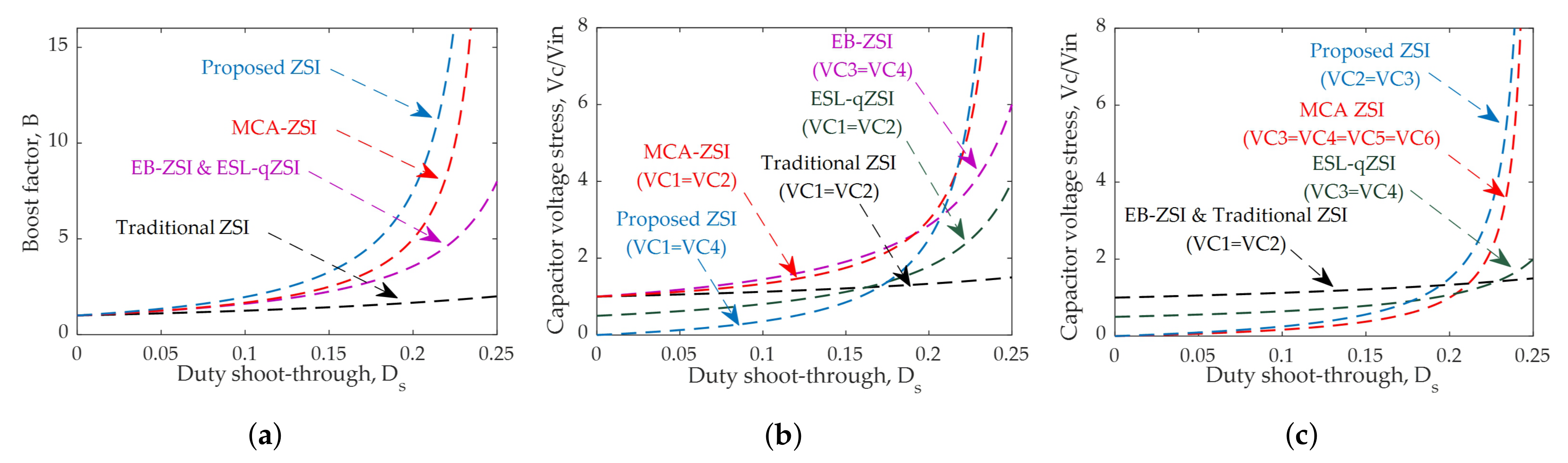
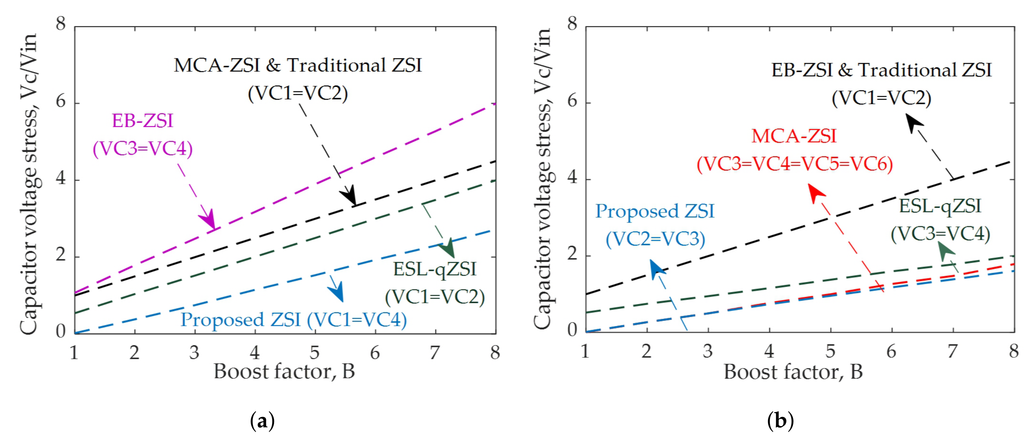
  • The analytical models reveal several advanced features of the proposed topologies such as the reduced capacitor voltage stress for the same boost factor; improved boosting capability for the same input voltage and shoot-through duty ratio, improved efficiency, reduced inrush current, and significantly improved dynamic voltage compensation capability as compared to all existing topologies.
The rest of the paper is organized as follows. The operating characteristic of the proposed topology is discussed in Section 2 and the detailed mathematical analysis associated with the proposed SL-SBZSI is presented in Section 3. The simple boost PWM scheme for the proposed topology is discussed in Section 4. The comparative results of the proposed scheme in comparison with different traditional topologies are provided in Section 5. The power loss calculation and efficiency analysis are demonstrated in Section 6. Simulation results with different case studies are presented in Section 7 by comprising with conventional MCA-ZSI. Finally, the experimental result is provided in Section 8 and the paper concluded in Section 9.

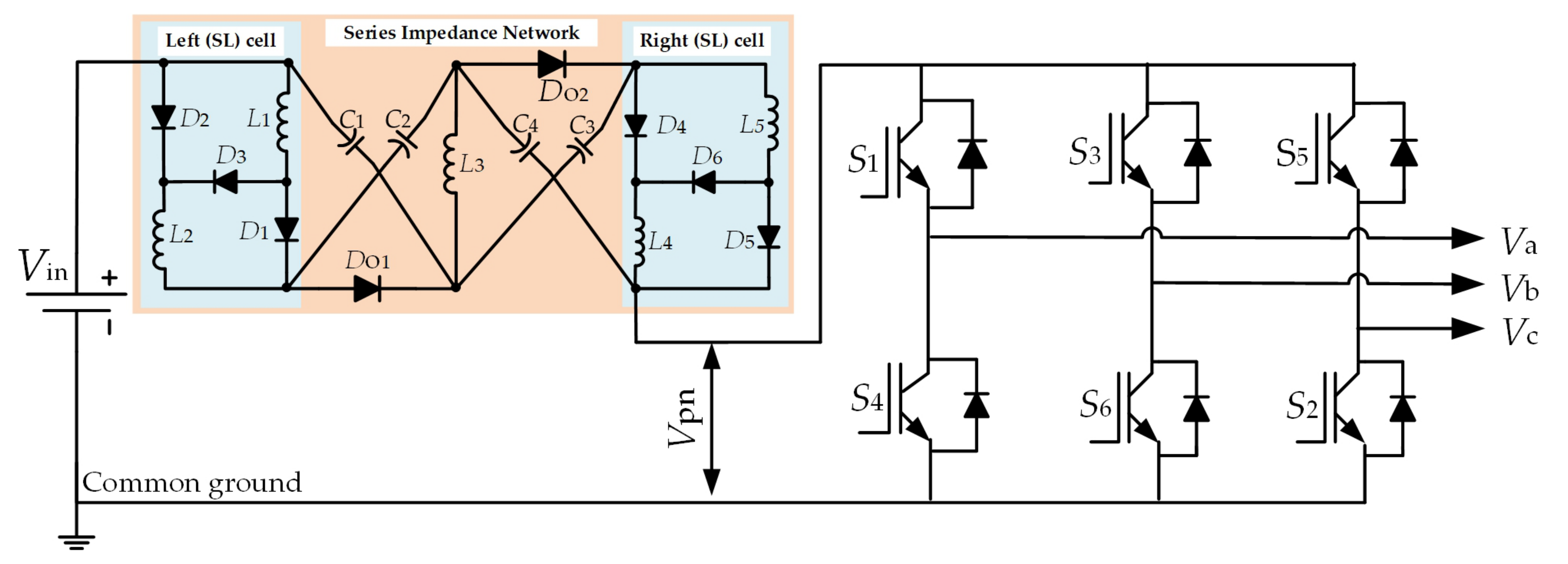
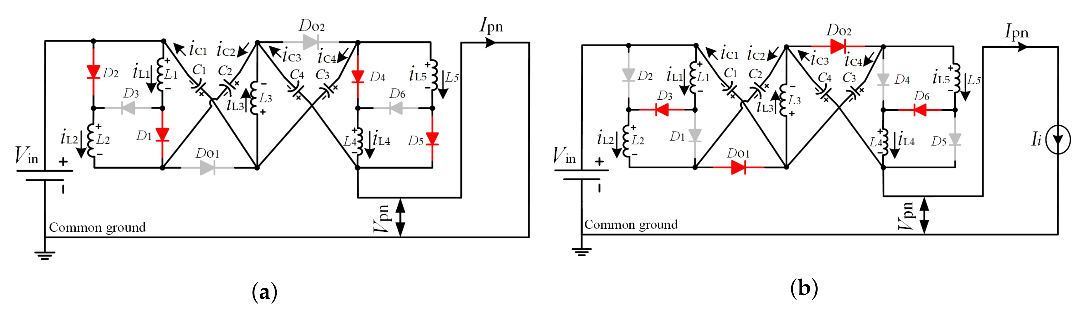
2. Operating Characteristics of the Proposed SL-SBZSI Topology

The circuit configuration of the proposed topology is shown in Figure 1. The impedance network of this topology is placed in series with the input DC-side and there is a common ground between this input and the output inverter. There are two switched inductor (SL) cells: one on the left and another right part of the impedance network which are used for improving the boost capability. The left cell includes inductors ( L 1 and L 2 ) and diodes ( D 1 , D 2 , and D 3 ) whereas the right cell includes inductors ( L 4 and L 5 ) , diodes ( D 4 , D 5 , and D 6 ) . The voltages V C 1 and V C 4 across capacitors C 1 and C 4 , respectively are same, i.e., V C 1 = V C 4 and similarly, V C 2 = V C 3 which are voltages across C 2 and C 3 , respectively. The operating characteristics of the proposed SL-SBZSI can be characterized in a similar manner to that of traditional ZSIs which have shoot and non-shoot through modes. These operating modes are discussed in the following subsections based on the corresponding equivalent circuits as shown in Figure 2a,b, respectively.

2.1. Shoot-Through Operating Mode

During the shoot-through (ST) operating mode, all semiconductor switches, i.e., S 1 to S 6 remain closed which can also be seen from Figure 2a. In this situation, the DC-link voltage becomes zero while diodes D 01 and D 02 remain open due to the reverse bias condition. The left and right SL cells are switched to a parallel configuration as diodes D 1 , D 2 , D 4 and D 5 are forward-biased. This operating mode allows to discharge capacitors C 1 , C 2 , C 3 and C 4 for which all currents through inductors L 1 , L 2 , L 3 and L 4 increase from their minimum to maximum values.
The relationships among voltages across different points and currents through different elements can be obtained by applying Kirchhoff’s voltage law (KVL) and Kirchhoff’s current law (KCL), respectively. By applying KVL in Figure 2a, the inductor voltages across all inductors can be written as follows:
V L 1 = V i n + V C 2 + V C 4 ; V L 1 = V L 2 = V L 4 = V L 5
V L 3 = 3 ( V i n 2 + V C 2 ) ,
where V L 1 is the voltage across L 1 , V L 2 is the voltage across L 2 , V L 3 is the voltage across L 3 , V L 4 is the voltage across L 4 , V L 5 is the voltage across L 5 , and V i n is the input voltage.
By applying KCL in Figure 2a, the currents flowing through capacitors can be written as follows:
I C 1 = 2 I L 1 I p n
I C 2 = 2 I L 1
where I C 1 is the current flowing through C 1 , I C 2 is the current flowing through C 2 , I L 1 is the current flowing through L 1 , and I p n is the shoot-through current.
The non-shoot-through operating mode, which is also known as the normal PWM mode or state, is discussed in the following subsection.

2.2. Non-Shoot-Through Operating Mode

During the non-shoot-through operating mode, the proposed SL-SBZSI acts like a traditional voltage source inverter as shown in Figure 2b. In this mode, the proposed topology generates the AC output voltage with the common complementary fashion of semiconductor switches. In this mode, diodes D 01 and D 02 become closed due to the forward bias condition. Furthermore, this operating mode enables D 3 and D 6 into the forward bias while the remaining diodes, i.e., D 1 , D 2 , D 4 and D 5 into the reverse bias for which inductors in both left and right SL cells are switched to series configurations. During this operating mode, all inductors and the input DC source supply power to the inverter. This means that the currents through inductor decrease and the voltages across the capacitor increase.
The relationships among voltages and currents in this operating mode can be obtained in a similar way to that of the shoot-through operating mode as discussed in the previous subsection, i.e., by applying KVL and KCL. By applying KVL in Figure 2b, the inductor voltages across all inductors can be written as follows:
V L 1 = V C 4 2 ; V L 1 = V L 2 = V L 4 = V L 5
V L 3 = V C 2
By applying KCL in Figure 2b, the currents flowing through capacitors can be written as follows:
I C 1 = I L 1 I i
I C 2 = I L 3 I i 2
where I L 3 is the current flowing through L 3 and I i is the DC-link current during non-shoot-through state.
These operating characteristics are used to analyze the performance of the proposed SL-SBZSI. The performance characteristics of the proposed topology also require to have the mathematical model, analysis for the ripple in the inductor current, ripples in the voltages across capacitors, and inverter switching device power. All these are discussed in the following section.

3. Performance Characteristics of Proposed SL-SBZSI

This section provides the theoretical frameworks for analyzing the steady-state performance characteristics of the proposed topology. The theoretical frameworks are mainly based on the mathematical model, nature of the ripple current, ripples in the voltage across capacitors, and the inverter switching device power. The mathematical model of the proposed SL-SBZSI is presented in the following subsection.

3.1. Mathematical Modeling of Proposed SL-SBZSI

The mathematical model for the steady-state analysis is developed in this subsection and the key switching waveforms for the proposed SL-SBZSI is shown in Figure 3. During the steady-state condition, the average inductor voltage should be zero over a complete switching period as per the volt-sec balance principle. Thus, the inductor voltage, by using volt-sec balance principle for the proposed SL-SBZSI, can be expressed through the following equation:
V L ( O N ) . D S . T S + V L ( O F F ) ( 1 D S ) . T S T S = 0
where D S is the shoot-through duty ratio and T S is the sampling time.
By using Equations (1) and (5) for V L 1 , it can be written as:
( V i n + V C 2 + V C 4 ) . D S . T S + ( V C 4 2 ) ( 1 D S ) . T S T S = 0 .
By using Equations (2) and (6) for V L 3 , it can be expressed as:
( 3 V i n 2 + 3 V C 2 ) . D S . T S + ( V C 2 ) ( 1 D S ) . T S T S = 0 .
By solving Equation (10) for the voltage across capacitor V C 4 , it can be written as follows:
V C 1 = V C 4 = 2 D S ( V i n + V C 2 ) ( 1 3 D S ) .
Similarly, the solution of Equation (11) for the voltage across capacitor V C 2 can be written as:
V C 2 = V C 3 = 3 D S . V i n 2 ( 1 4 D S ) .
Substituting Equation (13) into Equation (12), the equation for V C 4 can be simplified as:
V C 1 = V C 4 = D S ( 2 5 D S ) . V i n ( 1 7 D S + 12 D S 2 ) .
The peak DC-link voltage ( V ^ p n ) during the non-shoot-through mode can be written as follows:
V ^ p n = 2 V C 1 + V C 2 + V i n .
Substituting Equations (13) and (14) into Equation (15), the peak DC-link voltage can be obtained as follows:
V ^ p n = ( 2 3 D S 5 D S 2 ) . V i n 2 ( 1 7 D S + 12 D S 2 ) .
The boost factor, B for the proposed SL-SBZSI can be written as the ratio of V ^ p n to V i n and this can be written as follows:
B = V ^ p n V i n = ( 2 - 3 D S 5 D S 2 ) 2 ( 1 7 D S + 12 D S 2 ) .
The boost factor and the capacitor voltage stress with variations in the shoot-through duty ratio are shown in Figure 4a–c, respectively. From these figures, it can be clearly seen that there is a fast increase in the boost factor and capacitor voltage stresses for a small duty ratio, especially when the shoot-through duty ratio is higher than 0.2. By considering the lossless condition, it can be written as:
P i n = V i n . I i n = P o u t = V p h . I i I i n = I L 1 = V p h . I i V i n ,
where P i n is the input DC power, I i n is the input current, I L 1 is the inductor current, I i is the output current and V p h is the output AC phase voltage. The input current can be expressed in terms of the load and AC voltage as V p h = I i R L where R L is the load resistance. By substituting the relation in Equation (18), it can be rewritten as follows:
I L 1 = ( V p h ) 2 V i n . R L .
The input DC and output AC voltages can be expressed in terms of the modulation index and boost factor which can be written as follows:
V p h = 1 2 . ( M B V i n 2 ) ,
where M is the modulation index. By using Equation (20), the inductor current in Equation (19) can be rewritten as follows:
I L 1 = [ 1 2 ( M B . V i n 2 ) ] 2 V i n . R L .
According to the simple boost PWM control method, the relationship between the duty cycle and modulation index can be expressed as M = ( 1 D S ) . Using this relationship along with the substitution of Equation (17) into Equation (21) for three-phase proposed SL-SBZSI, it can be written as follows:
I L 1 = 3 ( 1 D S ) 2 ( 2 3 D S 5 D S 2 ) 2 . V i n 32 R L ( 1 7 D S + 12 D S 2 ) 2 .
During the shoot-through mode, the input current is zero for the proposed ZSI. At non-shoot-through mode, it can be expressed as the summation of the inductor and DC-link current as follows:
I i n = I L 1 + I i .
The performance characteristics of the proposed SL-SBZSI is analyzed by considering this mathematical model.

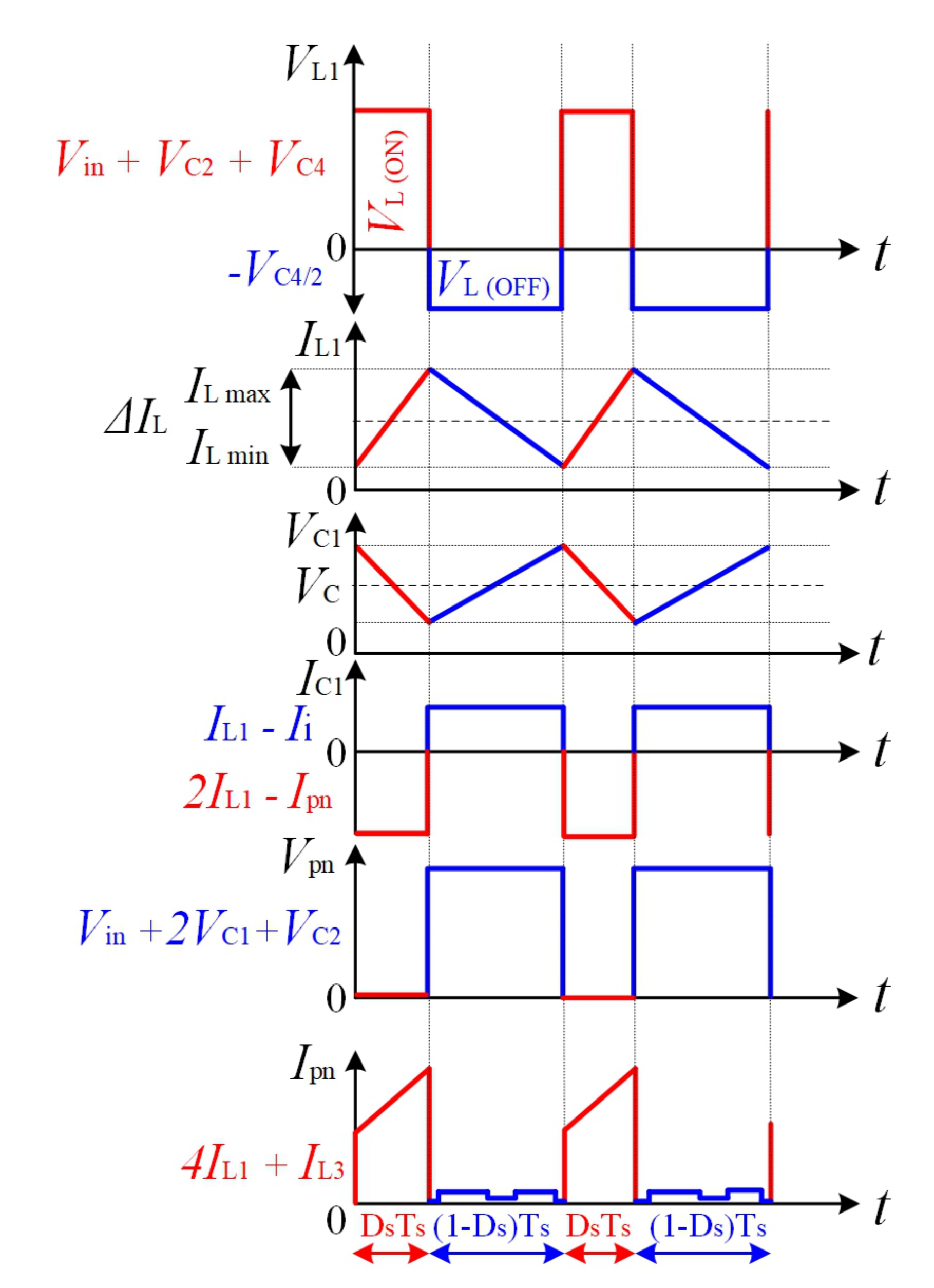
3.2. Analysis of Ripples in the Inductor Current for the Proposed SL-SBZSI

It is well known that the voltage across the inductor ( v L ) depends on the changes in the current flowing through the inductor which can be written as follows:
v L = L d i L d t ,
where i L is the current flowing through an inductor L. This voltage can be expressed in terms of the small changes in the current, i.e., the ripple current ( Δ i L ). For this purpose, the inductor voltage can be expressed as V L which is actually the average value of v L . If Δ t is considered is a small period, the average value of the voltage in Equation (24) can be written as follows:
V L = L Δ i L Δ t .
From Equation (25), the ripple in the current through L 1 can be written as follows:
Δ i L 1 = V L 1 L Δ t .
From Equation (1), it can be seen that V L 1 = V i n + V C 2 + V C 4 during the shoot-through operating mode. Hence, the ripple in i L 1 in Equation (26) during the shoot-through mode can be written as follows:
Δ i L 1 ( S T ) = V i n + V C 2 + V C 4 L Δ t ( S T ) .
In the simple boost control, each switching cycle contains two shoot-through pulses and thus, the duration per shoot-through, Δ t ( S T ) , is D S . T S 2 . Using this, Equation (27) can be written as follows:
Δ i L 1 ( S T ) = V i n + V C 2 + V C 4 L . D S . T S 2 .
Substituting the values of V C 2 and V C 4 from Equations (13) and (14), respectively into Equation (28); it can be written as follows:
Δ i L 1 ( S T ) = D S ( D S 1 ) ( 5 D S 2 ) . V i n 4 f S L 1 ( 1 7 D S + 12 D S 2 ) ,
where f S = 1 / T S is the sampling frequency.
From Equation (5), it can be seen that V L 1 = V C 4 2 during the non-shoot-through operating mode. Hence, the ripple in i L 1 in Equation (26) during this non-shoot-through mode can be written as follows:
Δ i L 1 ( n S T ) = V C 4 2 L Δ t ( n S T ) .
In the simple boost control, the duration per non-shoot-through, Δ t ( n S T ) , is ( 1 D S ) . T S 2 . Using this, Equation (30) can be written as follows:
Δ i L 1 ( n S T ) = V C 4 2 L . ( 1 D S ) . T S 2 .
Substituting the value of V C 4 from Equation (14) into Equation (31), it can be written as follows:
Δ i L 1 ( n S T ) = D S ( D S 1 ) ( 5 D S 2 ) . V i n 4 f S L 1 ( 1 7 D S + 12 D S 2 ) .
From Equations (29) and (32), it can be seen that the ripple currents in i L 1 during the shoot and non-shoot-through operating modes are the same. This statement is true for all currents flowing through different inductors though the amount of ripple can be different. To further justify this statement, the ripple currents in i L 3 , i.e., the current flowing through L 3 during both shoot and non-shoot-through operating modes are calculated here.
During the shoot-through mode, the ripple in i L 3 can be written as follows:
Δ i L 3 ( S T ) = V L 3 ( S T ) L . D S . T S 2 .
From Equation (2), it can be seen that V L 3 = 3 V i n 2 + V C 2 during the shoot-through operating mode. Hence, the ripple in i L 3 in Equation (33) during the shoot-through mode can be written as follows:
Δ i L 3 ( S T ) = 3 V i n + 6 V C 2 2 L . D S . T S 2
Substituting the value of V C 2 from Equation (13) into Equation (34), it can be written as follows:
Δ i L 3 ( S T ) = 3 D S ( 1 D S ) . V i n 4 f S L 3 ( 1 4 D S ) .
During the non-shoot-through mode, the ripple in i L 3 can be written as follows:
Δ i L 3 ( S T ) = V L 3 ( n S T ) L ( 1 D S ) . T S 2 .
From Equation (6), it can be seen that V L 3 = V C 2 during the non-shoot-through operating mode. Hence, the ripple in i L 3 in Equation (36) during the non-shoot-through mode can be written as follows:
Δ i L 3 ( n S T ) = V C 2 L ( 1 D S ) . T S 2 .
Substituting the value of V C 2 from Equation (13) into Equation (37), it can be written as follows:
Δ i L 3 ( n S T ) = 3 D S ( 1 D S ) . V i n 4 f S L 3 ( 1 4 D S ) .
Equations (35) and (38) clearly indicate that the ripple currents in i L 3 during the shoot and non-shoot-through operating modes are the same. The ripples in the current through the inductors in the ZSI affect the performance of input sources (e.g., fuel cell, PV units, etc.) which are connected to this inverter. The trade-off for minimizing the mismatch between the fuel cell and air utilization in fuel cells directly links with the generation of ripple currents [37] and the reduction in the average output power of the PV unit increases the generation of the ripple current [38]. Depending on the application of the power conditioning system, a certain value of the ripple can be allowed in the current flowing through the inductor for the satisfactory operation which needs to be selected in a precise way. In [39], the value of the ripple in the current flowing through an inductor is selected for prototyping a 50-kW fuel cell-based ZSI by following the standard design criteria. For the proposed SL-SBZSI, the ripple current value for the inductors is chosen as 30% of its average inductor current. Furthermore, as part of the fundamental mathematical modeling, the ripples in the voltages across capacitors are analyzed in the following subsection.

3.3. Analysis of Ripples in the Capacitor Voltage for the Proposed SL-SBZSI

The ripples in the capacitor voltage can be calculated in a similar way as presented in the previous subsection. The charging current flowing through the capacitor ( i C ) can be written as follows:
i C = C d v C d t ,
where v C is the voltage across the capacitor C. This current can be expressed in terms of the small changes in the voltage, i.e., the ripple voltage ( Δ v C ) . For this reason, the capacitor current can be expressed as I C which is actually the average value of i C . When Δ t is taken as a small period, the average capacitor current can be written as follows:
I C = C Δ v C Δ t .
From Equation (40), the ripple voltage of capacitor C 1 can be written as follows:
Δ v C 1 = I C 1 C Δ t .
From Equation (3), it can be seen that I C 1 = 2 I L 1 I p n during shoot-through operating mode. Hence, the ripple in v C 1 in (41) during the shoot-through mode can be written as follows:
Δ v C 1 ( S T ) = 2 I L 1 I p n C Δ t ( S T ) .
Each switching cycle contains two shoot-through pulses and as stated in the in the previous subsection, the duration per shoot-through, Δ t ( S T ) is D S . T S 2 . Using this, Equation (42) can be written as follows:
Δ v C 1 ( S T ) = 2 I L 1 I p n C . D S . T S 2 .
By using Equations (3) and (7), the voltage ripples for capacitor C 1 and C 4 during the shoot-through and non-shoot-through modes can be derived as follows:
Δ v C 1 ( S T ) = Δ v C 4 ( S T ) = D S ( 2 I L 1 I p n ) 2 C f S .
Δ v C 1 ( n S T ) = Δ v C 4 ( n S T ) = ( 1 D S ) ( I L 1 I i ) 2 C f S .
The numerical values of ripples for voltages across C 1 and C 4 during the shoot and non-shoot-through modes are same though their expressions in Equations (44) and (45) appeared differently.
By applying the same process and using Equations (4) and (8), the voltage ripples for capacitor C 2 and C 3 during the shoot-through and non-shoot-through modes can be expressed as follows:
Δ v C 2 ( S T ) = Δ v C 3 ( S T ) = D S . I L 1 C f S .
Δ v C 2 ( n S T ) = Δ v C 3 ( n S T ) = ( 1 D S ) ( I L 3 I i ) 4 C f S .
The numerical values of ripples for voltages across C 2 and C 3 during the shoot and non-shoot-through modes will also be same though their expressions in Equations (46) and (47) look different. The purpose of these capacitors in the ZSI is to absorb the ripples in the current and maintain a constant voltage. In [39], the value of the ripple in the voltage across the capacitor is chosen 3% which is a standard allowable value for designing power converters. In this proposed ZSI, the value of capacitor voltage ripple is kept within the standard design value and which is 0.6%.

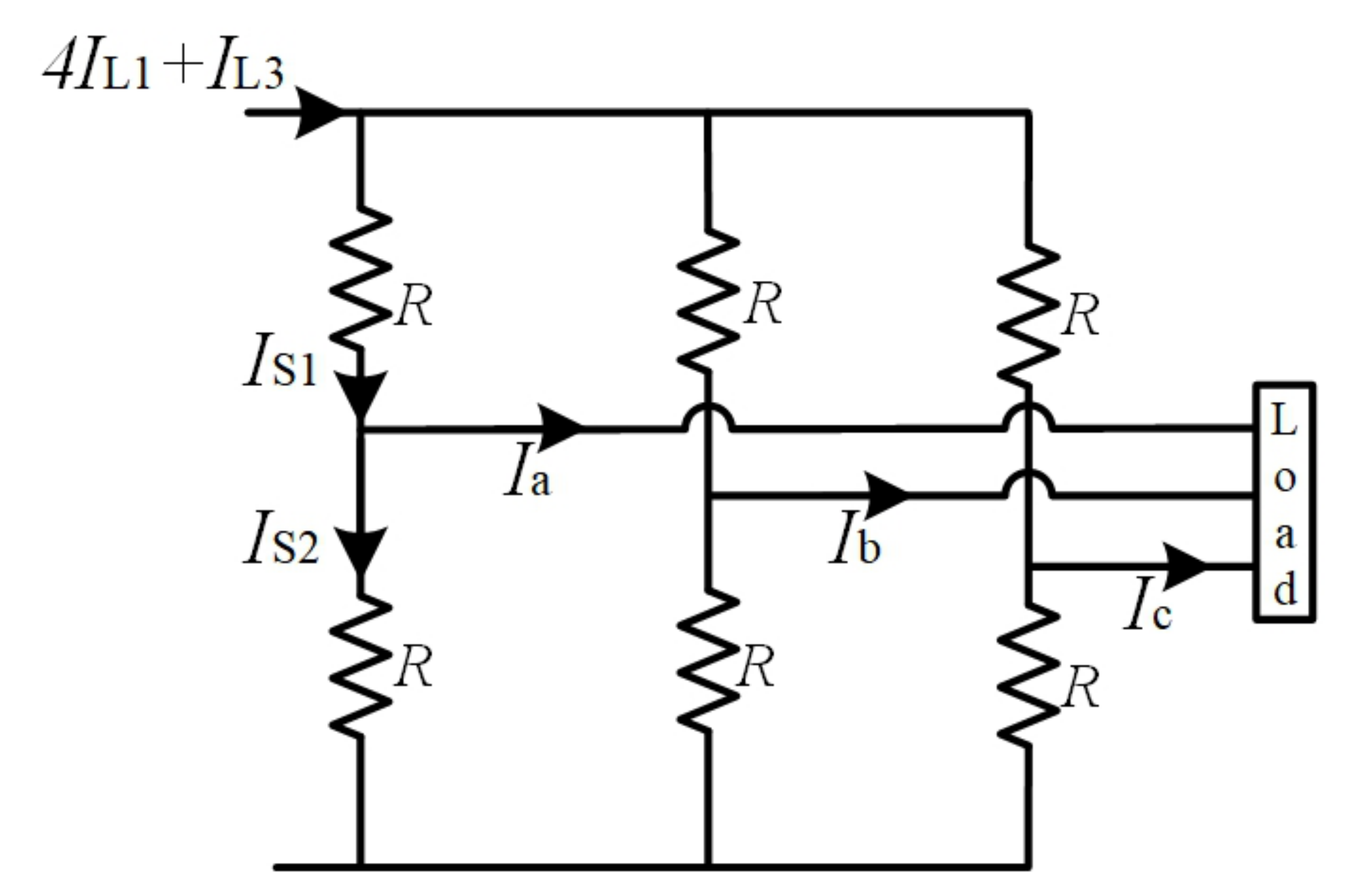
3.4. Inverter Switching Device Power

For any inverter, the semiconductor switches in the H-bridge circuit need to be selected in such a way that these switches can withstand the maximum impressed voltage while flowing the peak and average currents through these. The switching device power (SDP) is a measure which is used to determine the switching requirements according to generated voltage and current stress. The SDP is expressed in terms of the product of the voltage and current stress. Hence, the total SDP is measured as the cumulative SDP of all switching devices within the H-bridge circuit. As the total SDP indicates the size of the semiconductor device used in the circuit, it becomes an important cost index for the inverter. The average value of the total SDP ( S D P a v ) can be calculated as follows:
S D P a v = i = 1 N V i . I i a v ,
where N is the number of semiconductor devices within the H-bridge, V i is the impressed voltage on i-th device, and I i a v is the average current flowing through i-th device. Similarly, the peak value of the total SDP ( S D P P ) can be calculated as follows:
S D P P = i = 1 N V i . I i P
where I i P is the peak current flowing though i-th device.
The currents flowing through the inverter bridges during different operating modes mainly comprise of two components:
  • Current to load during the non-shoot-through mode and
  • Current through switches during the shoot-through mode.
The SDP is usually calculated by considering the shoot-through operation and the current paths for switches during the shoot-through operation is shown in Figure 5. From this figure, it can be seen that the current during this shoot-through mode is distributed into three parallel paths due to the symmetric structure of the H-bridge.
The current flowing through the inverter bridge is the sum of all currents flowing through the inductor. Hence the average current through each switch during the shoot-through mode can be written as follows:
I a v ( S T ) = 4 I L 1 + I L 3 3
The proposed topology acts as a traditional inverter during the non-shoot-through operation and hence, the average current during this non-shoot-through mode can be written as follows:
I a v ( n S T ) = 2 P o 3 V p h cos ϕ π . ( 1 D S ) ,
where V ^ p h is the output phase voltage, cos ϕ is the power factor of the load, and P o is the output power of the inverter. The output phase voltage of the inverter can be written as follows:
V ^ p h = M . V ^ p n 2 2 = M . B V i n 2 2
as V ^ p n = B V i n . Using Equation (52), Equation (51) can be written as follows:
I a v ( n S T ) = 2 . 2 2 P o 3 . B . V i n . M . cos ϕ π . ( 1 D S ) .
The overall average value of the current can be written as follows:
I a v = I a v ( S T ) + I a v ( n S T ) = 4 I L 1 + I L 3 3 . D S + 2 . 2 2 P o 3 . B . V i n . M . cos ϕ π . ( 1 D S ) .
The average value of the total SDP for the proposed inverter can be written as:
S D P a v = 6 . I a v . V ^ p n .
Substituting the value of I a v from Equation (54) and using V ^ p n = B V i n , Equation (55) can be rewritten as follows:
S D P ( A v e r a g e ) = 2 . B . V i n . ( 4 I L 1 + I L 3 ) . D S + 8 P o . ( 1 D S ) cos ϕ π M .
The switches conduct peak inverter current during the shoot-through mode. This peak current was calculated by assuming all switches within the H-bridge were ON and presenting these switches through pure resistors with the same value as shown in Figure 5. By applying KCL in Figure 5, it can be written as:
I S 1 + I S 2 = 2 ( 4 I L 1 + I L 3 ) 3
I S 1 I S 2 = I a ,
where I S 1 is the current flowing through the first switch, I S 2 is the current flowing through the second switch, and I a is the current flowing through line a. By solving Equations (57) and (58) for I S 1 , it can be written as follows:
I S 1 = 4 I L 1 + I L 3 3 + I a 2 .
The peak current flows through the first switch when the line current of the inverter is at its peak value, i.e., I a is at its peak. The peak value of I a can be written as:
I a ( P e a k ) = 2 P o 3 cos ϕ V ^ p h .
Substituting the value of V ^ p h from Equation (52) into Equation (59), it can be written as:
I a P = 4 P o 3 cos ϕ M . B . V i n
The peak value of the total SDP for the proposed inverter can be calculated as follows:
S D P P = 6 . I a P . V ^ p n .
Substituting the value of I a P from Equation (61) and using V ^ p n = B V i n , Equation (62) can be rewritten as follows:
S D P ( P e a k ) = 2 . B . V i n . ( 4 I L 1 + I L 3 ) + 4 P o cos ϕ M .
For selecting semiconductor devices in any power converter, the proper selection of the SDP is crucial as it is associated with the thermal requirement of the inverter. A detailed comparative study associated with the SDP for traditional and Z-source inverters is carried out in [40] where the average and peak SDP with the same specification are calculated. Equations (16) and (59) are the dominant parts of the final SDP model derived in (56) and (63) and can be used for the selection of semiconductor devices of proposed ZSI. Based on the application and peak power of the converter, the SDP requirement will vary as the peak current following through the semiconductor switches will vary and thus, the maximum voltages across these. Typically, the SDP is measured in KVA and the required KVA is generally chosen as a higher value than the calculated value.
All these performance characteristics are analyzed through rigorous simulation results in the later section. As the proposed topology uses a simple boost control method, it is discussed in the following section.

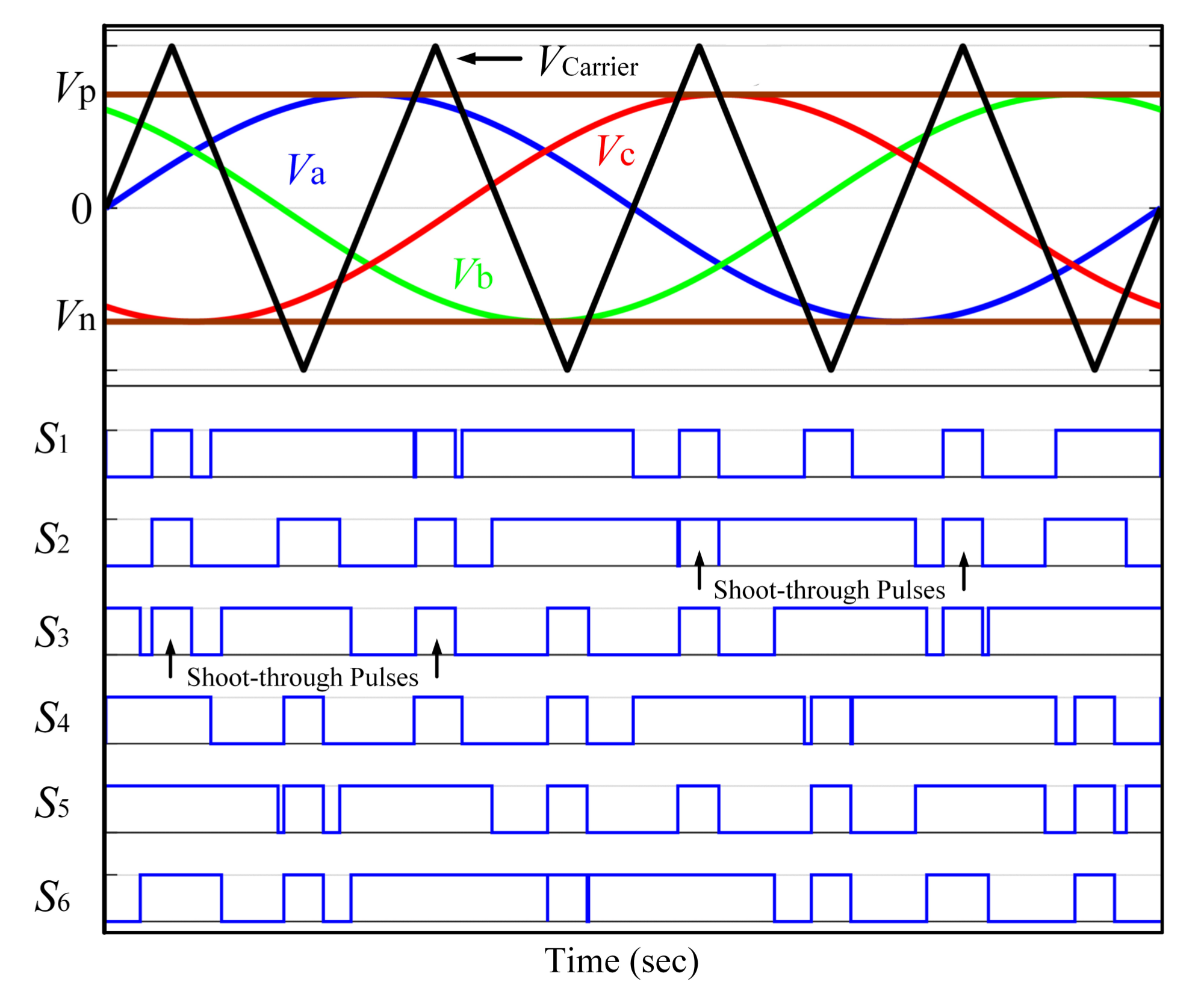
4. Inverter Switching Control Method

This section describes the PWM scheme to generate the shoot-through pulses. For the simplicity in control algorithm, the simple boost control (SBC) method as presented in [41] is used in this proposed topology. In the normal PWM scheme, the top and bottom switches of the inverter bridge legs are triggered in a complementary fashion when the triangular waveform V C a r r i e r is greater or lower than upper or lower values of the modulation waveforms V a , V b , and V c as shown in Figure 6.
In the SBC method, one positive DC waveform, V p and another negative DC waveform, V n are inserted to the traditional PWM scheme to control the shoot-through pulses. When the triangular carrier wave is greater than the positive DC waveform, first inverter bridge leg enters into the shoot-through state whereas another inverter bridge leg will enter into the shoot-through state when triangular carrier wave is lower than the negative DC waveform. This shoot-through can be generated through only one phase leg or the combination of any two legs or all three-phase legs of the inverter bridge. During zero state switching period of the traditional PWM control, the shoot-through pulses are placed into zero states which turn ON the semiconductor switches by keeping the active PWM states unchanged. Hence, the output sinusoidal voltage is maintained normally and at the same time, the inverter obtains high boosting capability by shooting through the DC-link voltage of the inverter. The switching pulses of the SBC with the shoot-through pulses for the three-phase inverter bridge are also depicted in Figure 6.
The voltage gain of the inverter can be written as follows [36]:
G = M × B .
Substituting Equation (17) to Equation (64), the voltage gain of the proposed inverter can be written as:
G = M × ( 2 3 D S 5 D S 2 ) 2 ( 1 7 D S + 12 D S 2 ) .
Since M = ( 1 D S ) for the SBC method, Equation (65) can be written as follows:
G = ( 1 D S ) ( 2 3 D S 5 D S 2 ) 2 ( 1 7 D S + 12 D S 2 ) ,
which represents the relationship between the voltage gain and the modulation index.
Figure 7 shows the voltage gain characteristics of the proposed SL-SBZSI along with different existing topologies with respect to the modulation index. From the characteristic curves in Figure 7, it can be clearly seen that the voltage gain significantly increased in the proposed SL-SBZSI as compared to other topologies while using the same value of the modulation index. The improved voltage gain characteristics of the proposed SL-SBZSI ensures the superiority over other existing ZSIs. A comparative study is presented to justify other steady-state characteristics, e.g., capacitor voltage stress with respect to the boost factor in the following section.

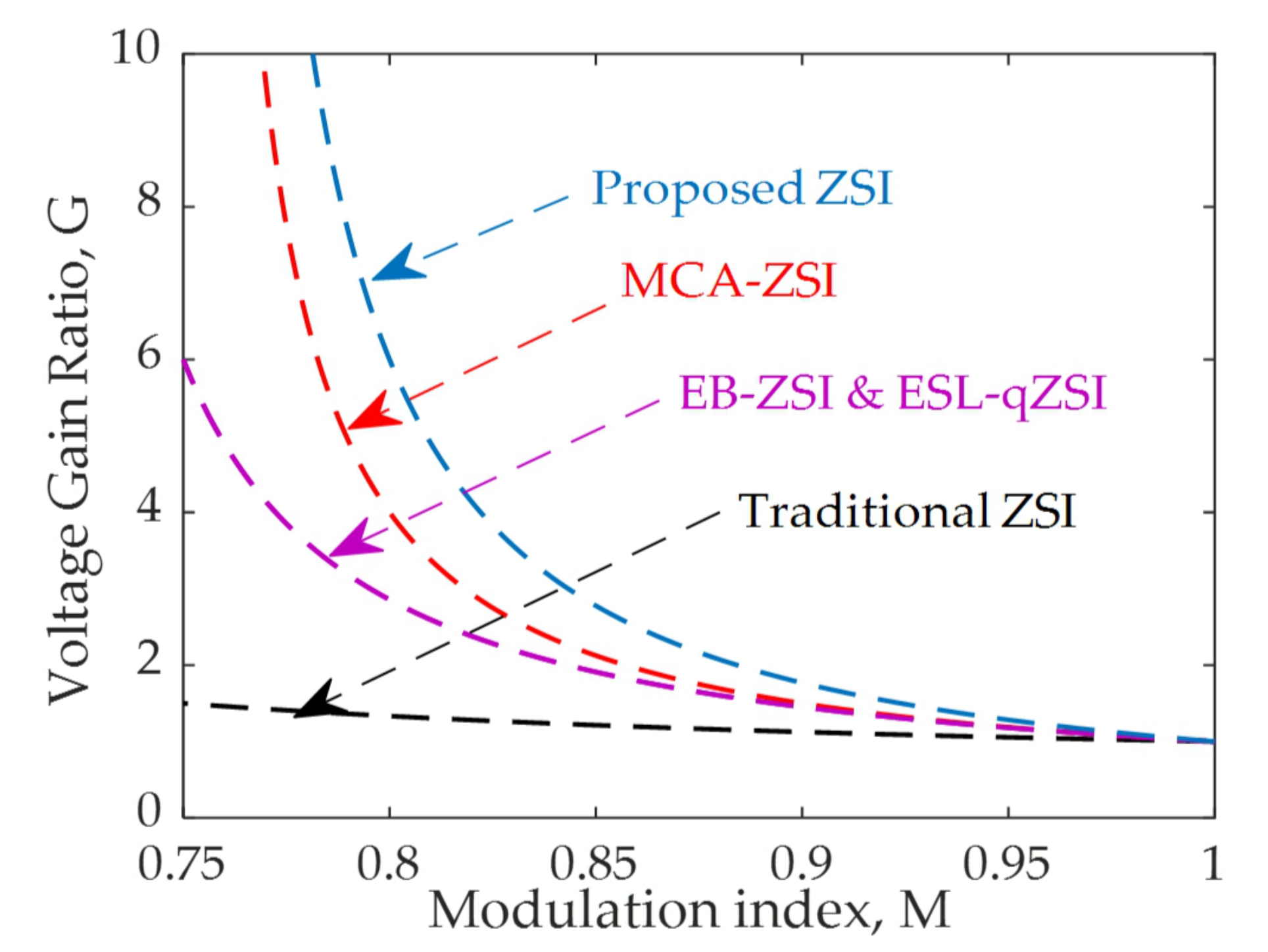
5. Comparative Analysis for the Capacitor Voltage Stress

This section presents a comparative analysis for the proposed SL-SBZSI against different existing topologies such as traditional ZSI, EB-ZSI, ESL-qZSI, and MCA-ZSI. As mentioned earlier, the proposed SL-SBZSI exhibits quite similar characteristics to that of an MCA-ZSI. Table 1 shows different factors associated with the performance of the proposed SL-SBZSI and MCA-ZSI. However, the comparative performance is analyzed against all above-mentioned topologies in terms of the capacitor voltage stress (both high and low stressed conditions) with variations in the boost factor. The capacitor voltage stresses for the high and low stressed capacitors are shown in Figure 8a,b, respectively. From these figures, it can be clearly seen that there are lower stresses on the capacitor voltages for the proposed topology as compared to all other topologies.

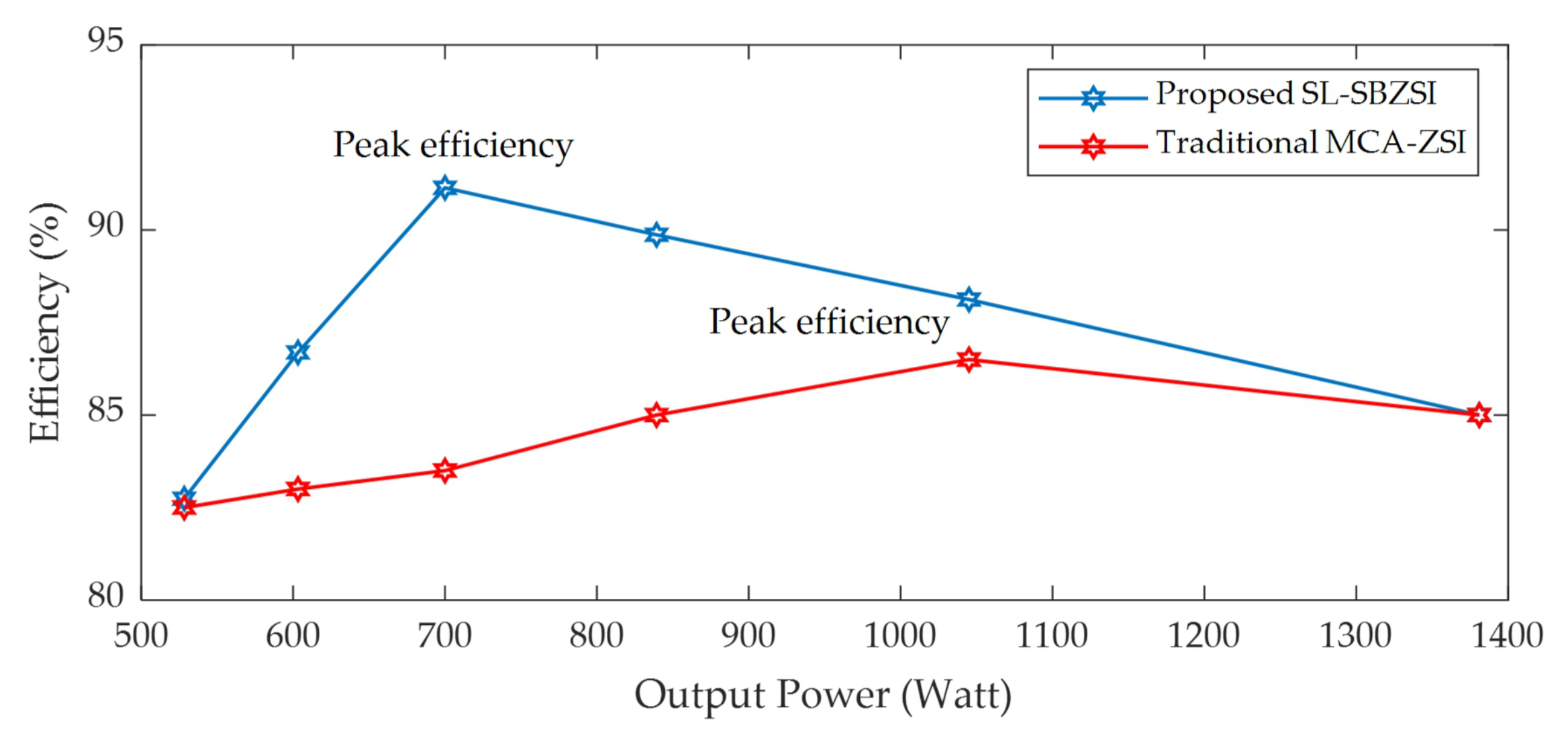
6. Calculation of Power Loss and Efficiency of the Proposed SL-SBZSI

The total power loss of the proposed SL-SBZSI is calculated based on the power loss in each component. In the proposed topology, there are some diodes which are ON during the shoot-through mode while remaining diodes are ON during the non-shoot-through operating mode. The input diodes ( D 01 and D 02 ) are on during the non-shoot-through mode and the power loss ( P D 01 , D 02 ) within these diodes can be calculated as follows:
P D 01 , D 02 = 2 [ v D . I i n + ( 1 D S ) . I i n 2 . r D + 2 M V ^ p h . I i n T s w 6 ] ,
where v D is the forward voltage drop across the diode, r D is the internal resistance of the diode, and T s w is the switching time.
The diodes ( D 3 and D 6 ) in the SL cells were also ON during the non-shoot-through mode and the power loss ( P D 3 , D 6 ) within these two diodes can be calculated as follows:
P D 3 , D 6 = 2 [ v D . ( 1 D S ) . I L 1 + ( 1 D S ) . I L 1 2 . r D + 2 V C 1 . I L 1 . T s w 6 ] .
During the shoot-through mode, diodes ( D 1 , D 2 , D 4 , and D 5 ) in the SL cells were ON and the power loss in these diodes can be written as:
P D 1 , D 2 , D 4 , D 5 = 4 [ v D . D S . I L 1 + D S . I L 1 2 . r D + V C 1 2 . I L 1 . T s w 6 ]
The power loss ( P L 1 , L 2 , L 4 , L 5 , L 3 ) in all inductors, i.e., L 1 , L 2 , L 4 , L 5 , and L 3 for the proposed topology can be counted as follows:
P L 1 , L 2 , L 4 , L 5 , L 3 = 4 [ I L 1 2 . r L ] + [ I L 3 2 . r L ] ,
where r L is the internal resistance of the inductor. Similarly, the power loss ( P C 1 , C 4 , C 2 , C 3 ) in all capacitors can be written as follows:
P C 1 , C 4 , C 2 , C 3 = 2 [ D S . I C 1 2 . r C + ( 1 D S ) . I C 1 2 . r C ] + 2 [ D S . I C 3 2 . r C + ( 1 D S ) . I C 3 2 . r C ] ,
where r C is the internal resistance of the capacitor.
The switching ( P s w ) and conduction ( P c o n d ) losses for the MOSFET switches can be expressed as follows [31]:
P s w = ( t o n + t o f f ) . f S . V o u t . ( 2 D S ) . I i n
P c o n d = r d s [ 2 3 . D S . ( 2 D S ) 2 . I i n 2 + 1.08 . ( 1 D S ) 3 . P o u t 2 M 2 . B 2 . V i n 2 ] ,
where t o n in the ON time of the switch, t o f f in the OFF time of the switch, r d s is the MOSFET drain to source resistance.
All these losses are used to calculate the total loss for the proposed SL-SBZSI and the efficiency is calculated based on these losses. The values of equivalent series resistors for the inductor and capacitor are obtained from BOURNS toroid inductor and KEMET (ELG108M200AT2AA) datasheets, respectively [42]. The internal resistance of the inductor ( r L ), which is also known as the equivalent series resistor (ESR) of the inductor, is chosen as 16 m Ω and the internal resistor of the capacitor, i.e., the ESR of the capacitor as 45 m Ω . The efficiency of the proposed topology is calculated by considering the diode model as MUR840G and the MOSFET model as STW45NM50.
The overall efficiency is shown in Figure 9, from where it can be noticed that the proposed inverter works in maximum efficiency of 91.14% at 700 W, whereas the traditional inverter has a maximum efficiency of 86.5% at 1045 W.

7. Simulation Results

The performance of the designed SL-SBZSI topology as shown in Figure 1 is verified through simulation results in Matlab/Simulink and compared with the existing MCA-ZSI topology. The SBC-based PWM scheme is adopted as a shoot-through control technique for both topologies. The parameters used for the simulation are listed in Table 2.
The simulation studies are carried out by considering the following four cases:
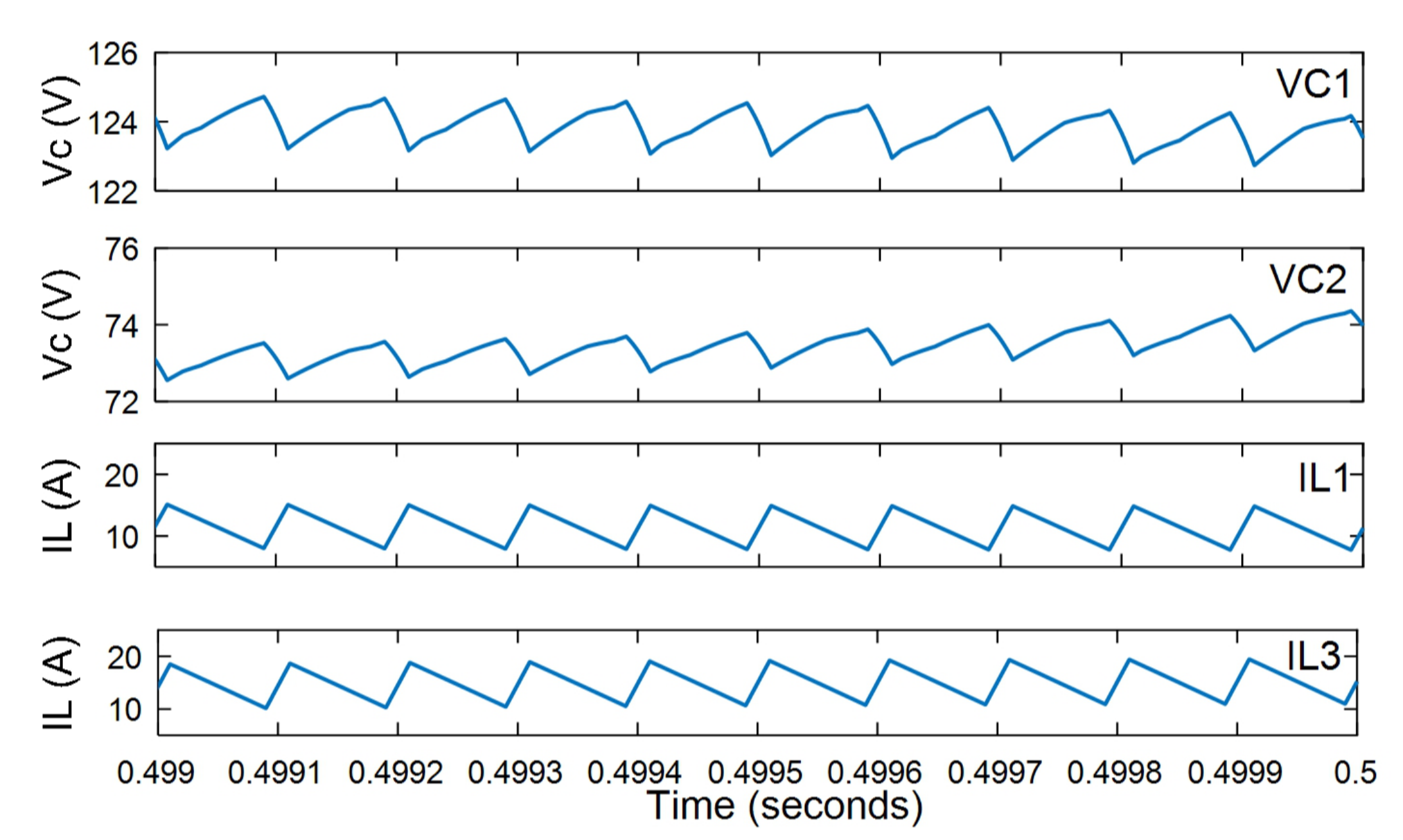
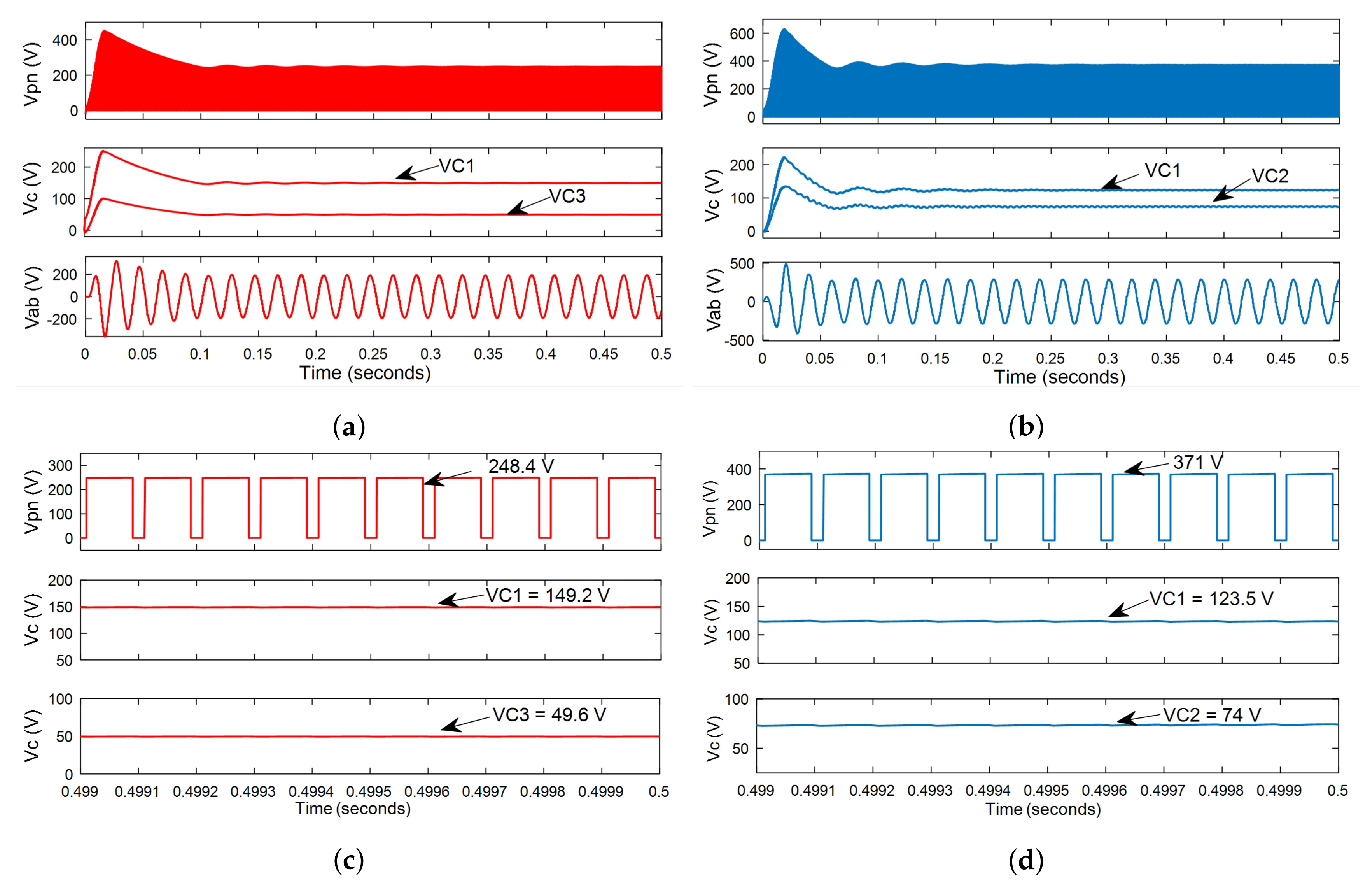
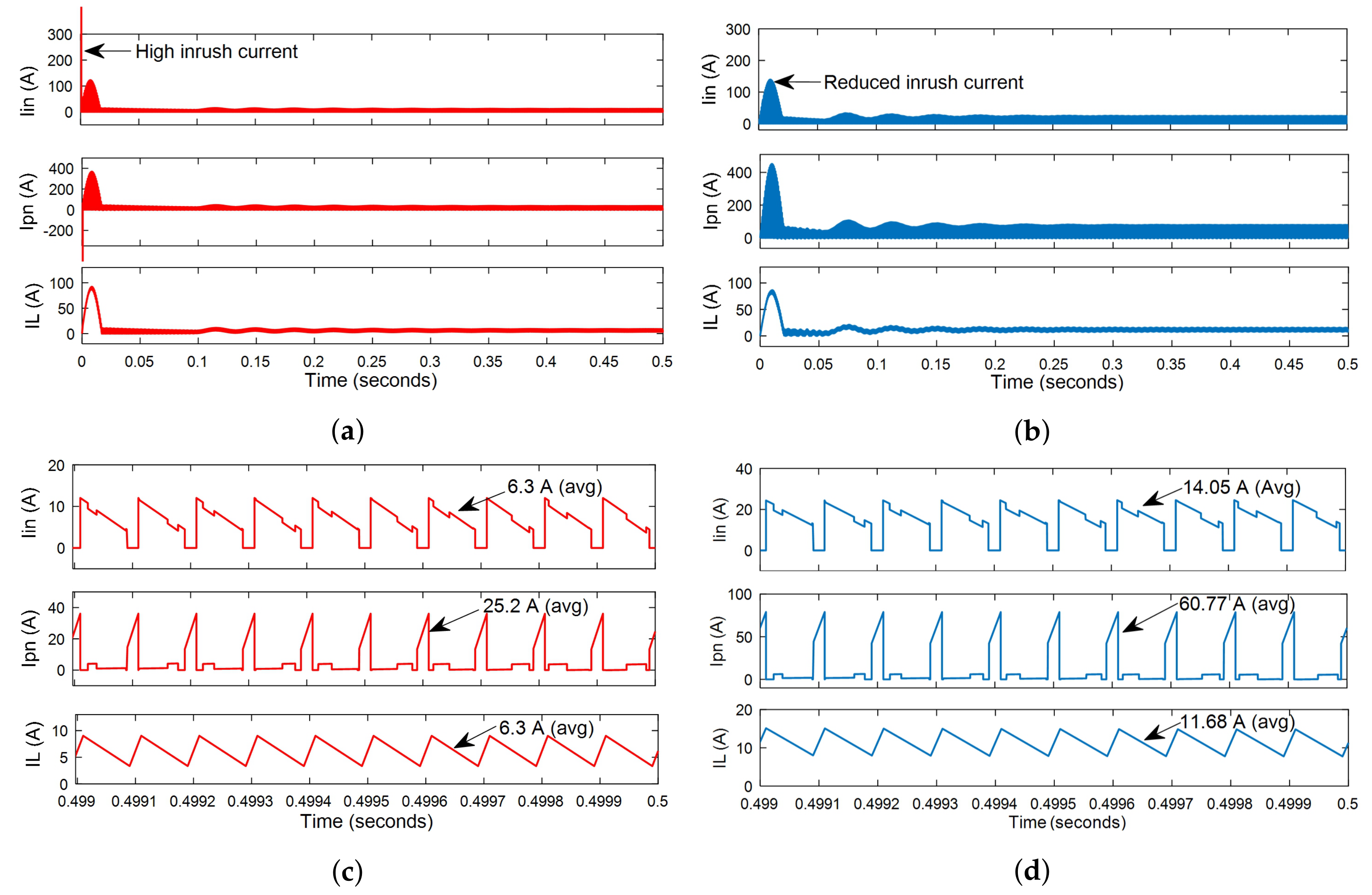
  • Analysis of the voltage and current characteristics with the fixed input voltage and shoot-through duty ratio.
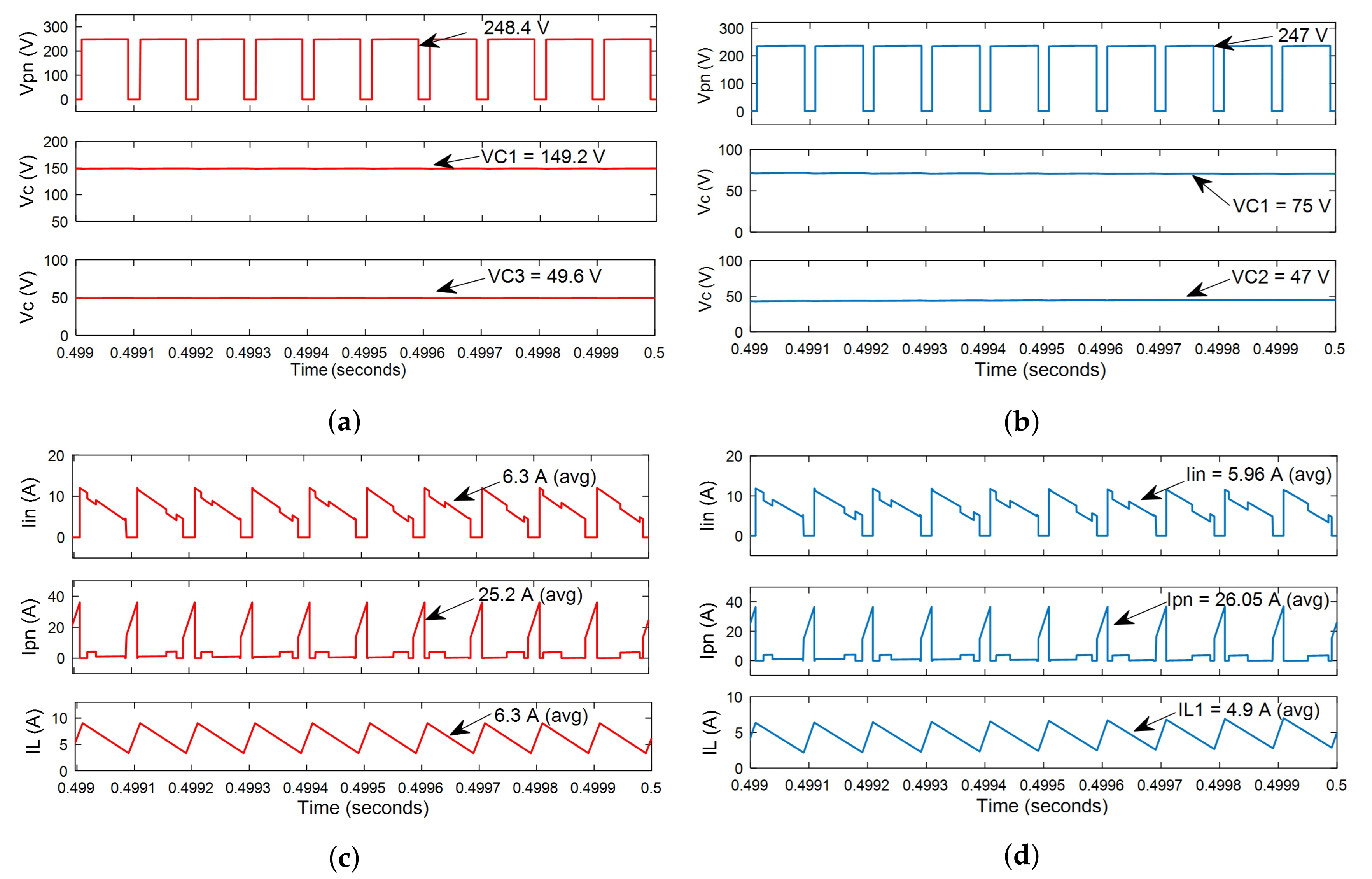
  • Analysis of the voltage and current characteristics with the fixed input voltage and boost factor but different shoot-through duty ratios.
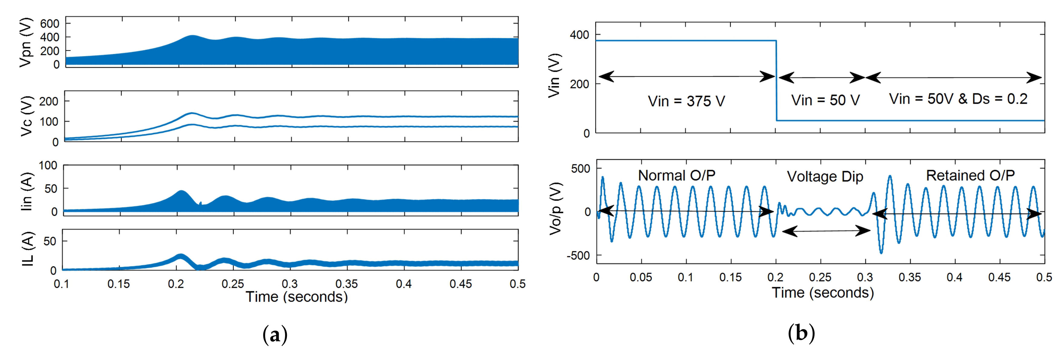
  • Analysis of the voltage and current characteristics with the fixed input voltage but slower variations in the shoot-through duty ratio.
  • Analysis of dynamic voltage compensation characteristics.
All these cases are discussed in the following with detailed analysis.
  • Case 1: analysis of the voltage and current characteristics with the fixed input voltage and shoot-through duty ratio.
In this case, the input voltage, V i n is considered as 50 V and the shoot-through duty ratio as D S = 0.2 for both the designed SL-SBZSI and existing MCA-ZSI. Under this condition, the voltage and current responses are observed for both SL-SBZSI and MCA-ZSI. The DC-link voltage V p n , the capacitor voltage V C , and the output load voltage ( V a b ) between phase a and phase b are shown in Figure 10a,b for the existing MCA-ZSI and designed SL-SBZSI, respectively. The corresponding enlarged versions of these responses are shown in Figure 10c,d, respectively.
From Figure 10c, it can be seen that the DC-link voltage of the existing MCA-ZSI boosted from 50 V to 248.4 V. Figure 10c also shows that the capacitor voltages for the MCA-ZSI corresponding to this condition are V C 1 = 149.2 V and V C 3 = 49.6 V while the rms value of the phase to phase voltage is obtained as 136 V, i.e., V a b ( r m s ) = 136 V as presented in Figure 10a. By using all these values, the boost factor (B) and the voltage gain (G) for the existing MCA-ZSI can be calculated as 4.96 and 3.97, respectively. The similar voltage responses for the designed SL-SBZSI can be seen from Figure 10b,d.
From Figure 10d, it can be seen that DC-link voltage of the designed SL-SBZSI boosted from 50 V to 371 V. Figure 10d also shows that the capacitor voltages for the SL-SBZSI corresponding to this condition are V C 1 = 123.5 V and V C 3 = 74 V while the rms value of the phase to phase voltage is obtained as 204 V, i.e., V a b ( r m s ) = 204 V as presented in Figure 10b. By using all these values, the boost factor (B) and the voltage gain (G) for the designed SL-SBZSI can be calculated as 7.42 and 5.93, respectively. From these analyses, it can be summarized that the designed topology improves the boost factor and voltage gain almost 1.5 times higher than an existing MCA-ZSI for the same input voltage and shoot-through duty ratio. Furthermore, the capacitor voltage reduces by around 17% for the high stressed capacitor in the designed SL-SBZSI as compared to the MCA-ZSI. However, the capacitor voltage increases by around 33% for the low stressed capacitor in the designed SL-SBZSI as compared to the MCA-ZSI.
Similarly, the input current I i n , the shoot-through current I p n , and the inductor current ( I L ) are shown in Figure 11a,b for the existing MCA-ZSI and designed SL-SBZSI, respectively. The corresponding enlarged version of these responses is shown in Figure 11c,d, respectively.
From Figure 11a,b, it can be seen that there exist input inrush current occurrence in both topologies. However, the inrush current in the designed SL-SBZSI is much lower than the existing MCA-ZSI. From Figure 11c, it can be seen that the average values of the input, shoot-through, and inductor currents for the existing MCA-ZSI are 6.3 A, 25.2 A, and 6.3 A, respectively. On the other hand, the average values of the input, shoot-through, and inductor currents for the designed SL-SBZSI are found 14.05 A, 60.77A, and 11.68 A, in Figure 11d respectively.
The ripples in the capacitor voltages and inductor are shown in Figure 12. From Figure 12, it can be seen that ripples of the capacitor voltages V C 1 and V C 2 are 0.75 V and 0.44 V, respectively while these values in the inductor currents I L 1 and I L 3 are 3.5 A and 4.2 A, respectively.
  • Case 2: analysis of the voltage and current characteristics with the fixed input voltage and boost factor but different shoot-through duty ratios.
In this case study, the input voltage and the boost factor are considered as same for both the existing MCA-ZSI and designed SL-SBZSI while using different shoot-through duty ratios. The value of the input voltage ( V i n ) and the boost factor (B) are considered as 50 V and 5, respectively. The values of the shoot-through duty ratio ( D S ) are considered as 0.2 and 0.18 for the existing MCA-ZSI and designed SL-SBZSI, respectively. The DC-link voltage, the high stressed capacitor voltage, and the low stressed capacitor voltage for the existing MCA-ZSI and designed SL-SBZSI are shown in Figure 13a,b, respectively.
From these figures, it can be seen that the values of these voltages for the MCA-ZSI are 248.4 V, 149.2 V, and 49.6 V, respectively; while these for SL-SBZSI are 247 V, 75 V, and 47 V, respectively. This situation clearly indicates that the input voltage is boosted to a similar value for both topologies. However, the capacitor voltage stresses are reduced for the designed SL-SBZSI as compared to the MCA-ZSI. Hence, it can be concluded that the designed topology exhibits lower capacitor voltage stresses as compared to the MCA-ZSI for the same boosting capability.
The corresponding input, shoot-through, and inductor currents for the existing MCA-ZSI and designed SL-SBZSI are shown in Figure 13c,d, respectively. From these figures, it can be seen that the average value of the shoot-through current for the designed SL-SBZSI is slightly higher than the MCA-ZSI. However, the input and inductor currents are lower in the designed SL-SBZSI as compared to the MCA-ZSI.
  • Case 3: analysis of the voltage and current characteristics with the fixed input voltage but slower variations in the shoot-through duty ratio.
This case study was used to analyze the impact of the inrush current while applying a fixed input voltage. The input voltage ( V i n ) is still considered as 50 V but the duty shoot-through ratio ( D S ) is slowly varied from 0 to 0.2 within 200 ms. In this way, the soft-start strategy is adopted which is an inherent characteristic of the designed SL-SBZSI. From Figure 14a, it can be seen that the slow increases in the shoot-through duty ratio from 0 to 0.2 within 200 ms, significantly reduces the inrush current and suppresses the resonance without any voltage and current surge. Therefore, it can be summarized that the designed SL-SBZSI does not exhibit high start-up inrush current.
  • Case 4: analysis of dynamic voltage compensation characteristics
In this case, the dynamic voltage compensation characteristic is examined by applying different input voltages within a period of 0.5 s. The designed SLSBZSI operates in the normal state from 0 to 0.2 s with a normal input voltage ( V i n ) of 375 V and generates a line to line rms voltage V a b ( r m s ) of 204 V.
At time, t = 0.2 s, the input inverter voltage drops down to 50 V and continues until t = 0.3 s. To further justify the boosting effect of the designed SL-SBZSI in terms of the dynamic voltage compensation capability, a shoot-through duty ratio ( D S ) of 0.2 is applied at t = 0.3 s. From Figure 14b, it can be observed that the output line voltage is successfully returned to 204 V. Hence, it can be summarized that the designed SL-SBZSI maintains the desired voltage level even for a lower input voltage while using a shoot-through duty ratio.

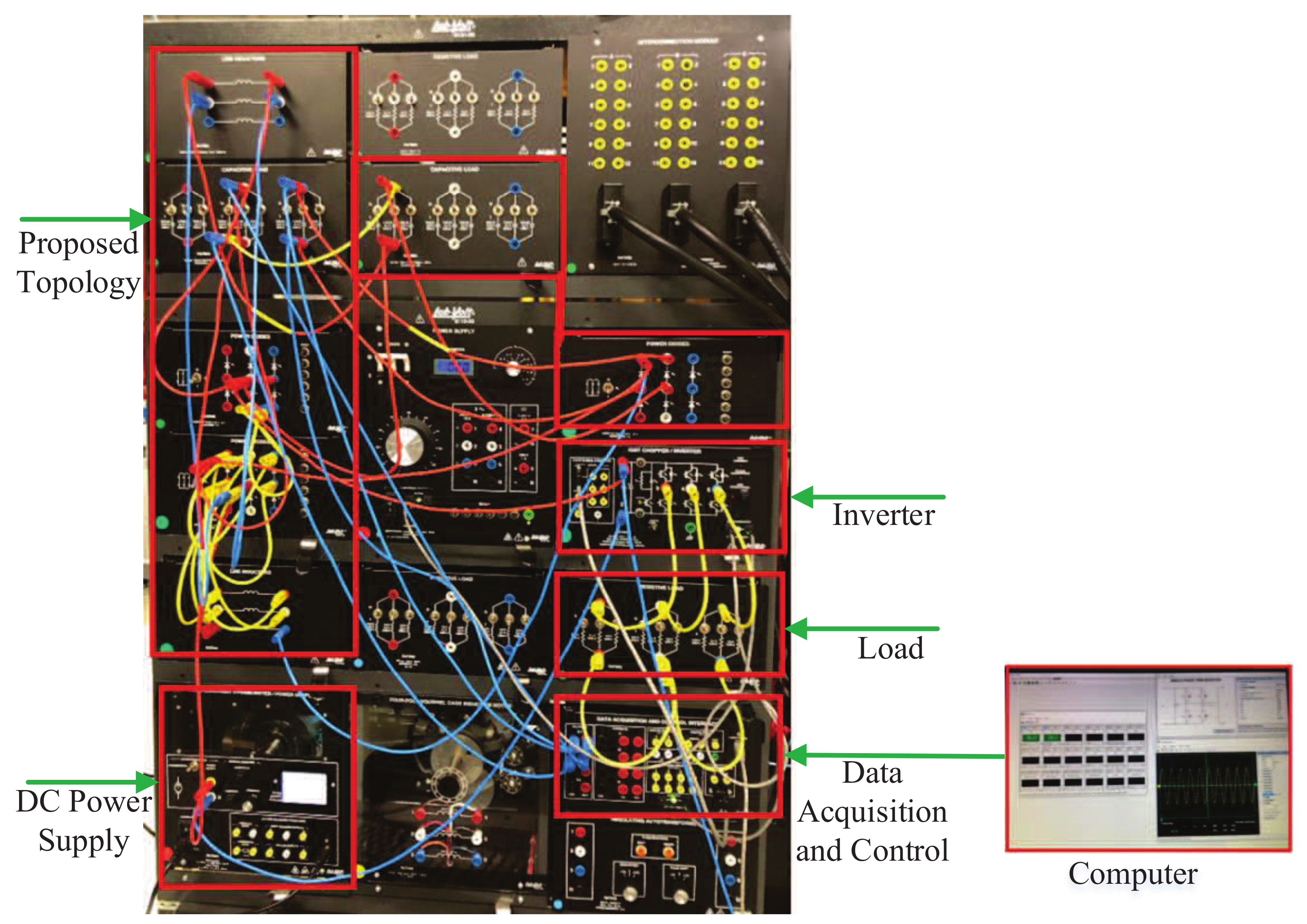
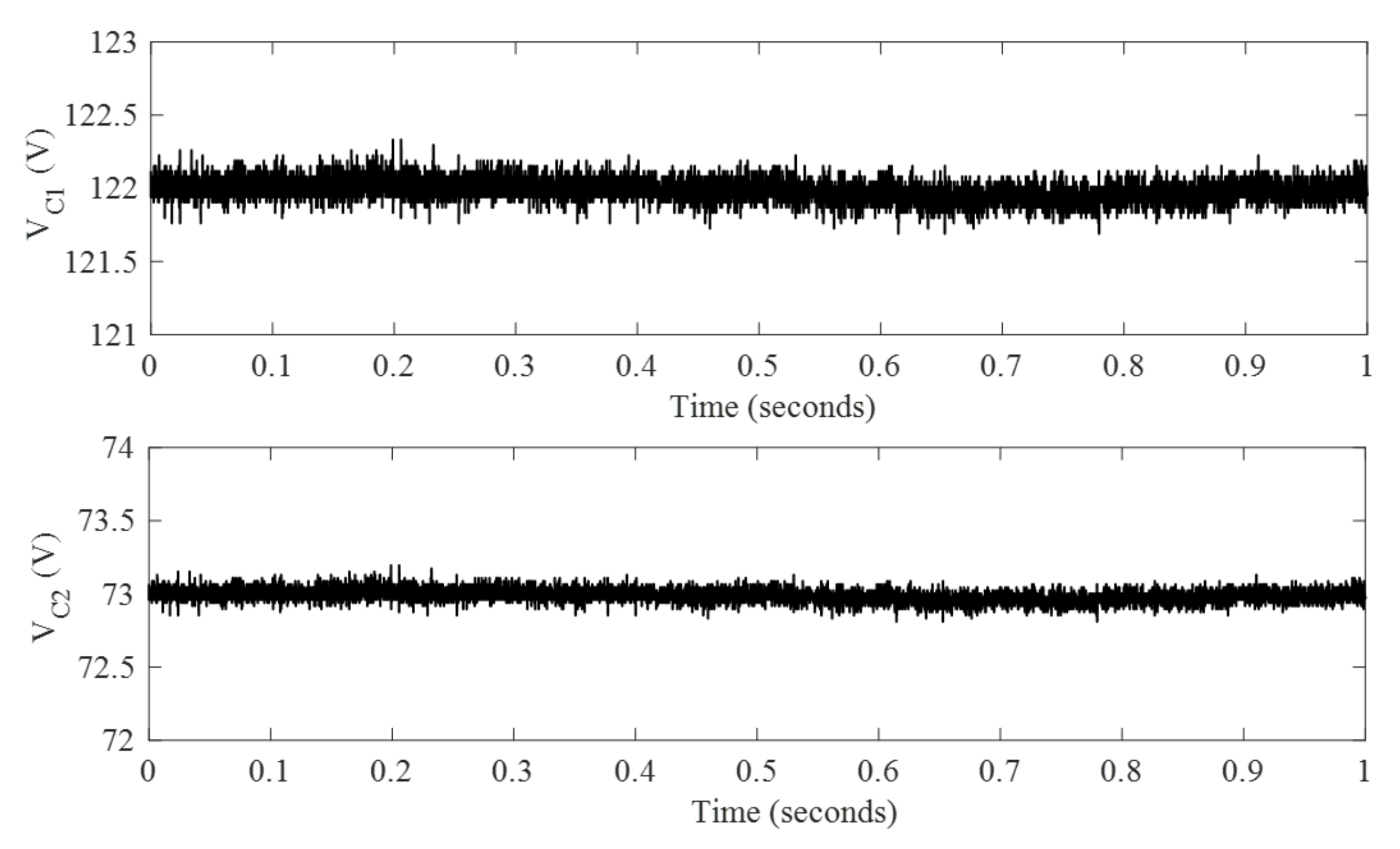
8. Experimental Validation

The proposed topology was also validated through experimental studies and the experimental setup is shown in Figure 15. The experimental setup looks quite similar to that as presented in [36] and the similar parameters are used for the experiment. For this reason, the parameters of the SL-SBZSI were not listed here in order to avoid repetition. However, Figure 15 shows the experimental setup for a three-phase inverter while it is for a single-phase in [36].
Another difference is the use of a PV emulator in [36] while the same component was used here as a fixed DC supply. In this experiment, the input DC voltage was used as 50 V while the shoot-through duty ratio is considered as 0.2 in order to make the scenario consistent with the simulation result as presented in Case 1. The experiment was conducted to observe the capacitor voltage stresses, i.e., the voltages across C 1 and C 2 . Figure 16 shows V C 1 and V C 2 which are actually the voltages across C 1 and C 2 , respectively for the proposed SL-SBZSI from where it can be seen that V C 1 = 122 V and V C 2 = 73 V with some ripples in these voltage responses. These results matched with the simulation results and hence, it can be said that the proposed topology reduces the capacitor voltage stresses significantly. Similarly, other responses, e.g., the output voltage of the inverter is also observed but it has not been presented here as it has already been discussed in [36].

9. Conclusions

A switched inductor-based simple boost ZSI (SL-SBZSI) is designed, which is driven by the low shoot-through duty ratio. From both analytical and simulation results, it can be concluded that the designed SL-SBZSI guarantees reduced capacitor voltage stresses for the same boost factor and input voltage; improved efficiency; very high boosting capability for the same input voltage and shoot-through duty ratio; reduced inrush current; and significantly improved dynamic voltage compensation capabilities during the sudden changes in the input voltage. The analytical results to validate the theories and simulation results under different cases clearly demonstrate the superiority of the designed SL-SBZSI as compared to all existing topologies within the same category. Experimental results support the theoretical and simulation results which clearly indicate the practical applicability of the newly developed topology. The dynamic voltage compensation characteristics of the designed SL-SBZSI also reduces the size and cost of the system as this will help to eliminate the use of transformers. Furthermore, the dynamic compensation capability of the designed SL-SBZSI makes it suitable for the renewable energy applications where the DC voltage input to the inverter changes frequently.

Author Contributions

Conceptualization, N.S.; Methodology, N.S.; Software, N.S.; Validation, N.S., M.A.M., T.K.R.; Formal analysis, N.S., M.A.M.; Investigation, N.S., M.A.M.; Resources, R.K., M.F.R.; Data curation, N.S.; Writing—original draft preparation, N.S., M.A.M.; Writing—review and editing, N.S., M.A.M.; Visualization, N.S., M.A.M.; Supervision, R.K., M.A.M., and M.F.R.; Project administration, R.K.; Funding acquisition, R.K.

Funding

The work was supported by the Graduate Assistantship (GA) scheme of Universiti Teknologi PETRONAS (UTP).

Conflicts of Interest

The authors declare no conflict of interest.

References

  1. Peng, F.Z. Z-source inverter. IEEE Trans. Ind. Appl. 2003, 39, 504–510. [Google Scholar] [CrossRef]
  2. Thangaprakash, S.; Krishnan, A. Implementation and critical investigation on modulation schemes of three phase impedance source inverter. Iran. J. Electr. Electron. Eng. 2010, 6, 84–92. [Google Scholar]
  3. Peng, F.Z.; Joseph, A.; Wang, J.; Shen, M.; Chen, L.; Pan, Z.; Ortiz-Rivera, E.; Huang, Y. Z-source inverter for motor drives. IEEE Trans. Power Electron. 2005, 20, 857–863. [Google Scholar] [CrossRef]
  4. Huang, Y.; Shen, M.; Peng, F.Z.; Wang, J. Z-Source Inverter for Residential Photovoltaic Systems. IEEE Trans. Power Electron. 2006, 21, 1776–1782. [Google Scholar] [CrossRef]
  5. Jung, J.W.; Keyhani, A. Control of a fuel cell based Z-source converter. IEEE Trans. Energy Convers. 2007, 22, 467–476. [Google Scholar] [CrossRef]
  6. Peng, F.Z.; Shen, M.; Holland, K. Application of Z-source inverter for traction drive of fuel cell—Battery hybrid electric vehicles. IEEE Trans. Power Electron. 2007, 22, 1054–1061. [Google Scholar] [CrossRef]
  7. Yu, Y.; Zhang, Q.; Liang, B.; Liu, X.; Cui, S. Analysis of a single-phase Z-source inverter for battery discharging in vehicle to grid applications. Energies 2011, 4, 2224–2235. [Google Scholar] [CrossRef]
  8. Zhou, Z.J.; Zhang, X.; Xu, P.; Shen, W.X. Single-phase uninterruptible power supply based on Z-source inverter. IEEE Trans. Ind. Electron. 2008, 55, 2997–3004. [Google Scholar] [CrossRef]
  9. Sonar, S.; Maity, T.; Minu, M. Single phase transformerless wide range ac boost voltage regulator based on z-source network. Int. J. Electr. Power Energy Syst. 2013, 47, 193–197. [Google Scholar] [CrossRef]
  10. Huang, S.; Zhang, Y.; Hu, S. Stator Current Harmonic Reduction in a Novel Half Quasi-Z-Source Wind Power Generation System. Energies 2016, 9, 770. [Google Scholar] [CrossRef]
  11. Priyadarshi, N.; Padmanaban, S.; Ionel, D.; Mihet-Popa, L.; Azam, F. Hybrid PV-Wind, Micro-Grid Development Using Quasi-Z-Source Inverter Modeling and Control—Experimental Investigation. Energies 2018, 11, 2277. [Google Scholar]
  12. Tang, Y.; Xie, S.; Zhang, C.; Xu, Z. Improved Z-source inverter with reduced Z-source capacitor voltage stress and soft-start capability. IEEE Trans. Power Electron. 2009, 24, 409–415. [Google Scholar] [CrossRef]
  13. Anderson, J.; Peng, F.Z. Four quasi-Z-source inverters. In Proceedings of the Power Electronics Specialists Conference, Rhodes, Greece, 15–19 June 2008; pp. 2743–2749. [Google Scholar]
  14. Loh, P.C.; Gao, F.; Blaabjerg, F. Embedded EZ-source inverters. IEEE Trans. Ind. Appl. 2010, 46, 256–267. [Google Scholar]
  15. Sun, D.; Ge, B.; Bi, D.; Peng, F.Z. Analysis and control of quasi-Z source inverter with battery for grid-connected PV system. Int. J. Electr. Power Energy Syst. 2013, 46, 234–240. [Google Scholar] [CrossRef]
  16. Tang, Y.; Wei, J.; Xie, S. Grid-tied photovoltaic system with series Z-source inverter. IET Renew. Power Gener. 2013, 7, 275–283. [Google Scholar] [CrossRef]
  17. Zhu, M.; Yu, K.; Luo, F.L. Switched inductor Z-source inverter. IEEE Trans. Power Electron. 2010, 25, 2150–2158. [Google Scholar]
  18. Gajanayake, C.J.; Luo, F.L.; Gooi, H.B.; So, P.L.; Siow, L.K. Extended-boost Z-source inverters. IEEE Trans. Power Electron. 2010, 25, 2642–2652. [Google Scholar] [CrossRef]
  19. Nguyen, M.K.; Lim, Y.C.; Choi, J.H. Two switched-inductor quasi-Z-source inverters. Iet Power Electron. 2012, 5, 1017–1025. [Google Scholar] [CrossRef]
  20. Deng, K.; Zheng, J.; Mei, J. Novel switched-inductor quasi-Z-source inverter. J. Power Electron. 2014, 14, 11–21. [Google Scholar] [CrossRef]
  21. Ho, A.V.; Chun, T.W.; Kim, H.G. Extended boost active-switched-capacitor/switched-inductor quasi-Z-source inverters. IEEE Trans. Power Electron. 2015, 30, 5681–5690. [Google Scholar] [CrossRef]
  22. Babaei, E.; Asl, E.S.; Babayi, M.H.; Laali, S. Developed embedded switched-Z-source inverter. IET Power Electron. 2016, 9, 1828–1841. [Google Scholar] [CrossRef]
  23. Subhani, N.; Kannan, R.; Romlie, M.F. Modified Topology of Z-Source Inverter by Switched Inductor with Series Impedance Network. In Proceedings of the 2018 International Conference on Intelligent and Advanced System (ICIAS), Kuala Lumpur, Malaysia, 13–14 August 2018; pp. 1–5. [Google Scholar] [CrossRef]
  24. Subhani, N.; Kannan, R.; Romlie, M.F. Steady state performance analysis of one switched inductor series Z-source inverter. In Proceedings of the 5th IET International Conference on Clean Energy and Technology (CEAT2018), Kuala Lumpur, Malaysia, 5–6 September 2018; pp. 1–6. [Google Scholar] [CrossRef]
  25. Strzelecki, R.; Adamowicz, M.; Strzelecka, N.; Bury, W. New type T-source inverter. In Proceedings of the Compatibility and Power Electronics, CPE’09, Badajoz, Spain, 20–22 May 2009 ; pp. 191–195. [Google Scholar]
  26. Zhu, M.; Li, D.; Loh, P.C.; Blaabjerg, F. Tapped-inductor Z-source inverters with enhanced voltage boost inversion abilities. In Proceedings of the 2010 IEEE International Conference on Sustainable Energy Technologies (ICSET), Kandy, Sri Lanka, 6–9 December 2010; pp. 1–6. [Google Scholar]
  27. Qian, W.; Peng, F.Z.; Cha, H. Trans-Z-source inverters. IEEE Trans. Power Electron. 2011, 26, 3453–3463. [Google Scholar] [CrossRef]
  28. Adamowicz, M.; Strzelecki, R.; Peng, F.Z.; Guzinski, J.; Rub, H.A. New type LCCT-Z-source inverters. In Proceedings of the 2011-14th European Conference on Power Electronics and Applications (EPE 2011), Birmingham, UK, 30 August–1 September 2011; pp. 1–10. [Google Scholar]
  29. Nguyen, M.K.; Lim, Y.C.; Kim, Y.G. TZ-source inverters. IEEE Trans. Ind. Electron. 2013, 60, 5686–5695. [Google Scholar] [CrossRef]
  30. Loh, P.C.; Li, D.; Blaabjerg, F. Γ-Z-source inverters. IEEE Trans. Power Electron. 2013, 28, 4880–4884. [Google Scholar] [CrossRef]
  31. Fathi, H.; Madadi, H. Enhanced-boost Z-source inverters with switched Z-impedance. IEEE Trans. Ind. Electron. 2016, 63, 691–703. [Google Scholar] [CrossRef]
  32. Abbasi, M.; Eslahchi, A.H.; Mardaneh, M. Two Symmetric Extended-Boost Embedded Switched-Inductor Quasi-Z-Source Inverter With Reduced Ripple Continuous Input Current. IEEE Trans. Ind. Electron. 2018, 65, 5096–5104. [Google Scholar] [CrossRef]
  33. Ho, A.V.; Chun, T.W. Modified Capacitor-Assisted Z-Source Inverter Topology with Enhanced Boost Ability. J. Power Electron. 2017, 17, 1195–1202. [Google Scholar]
  34. Yang, B.; Li, W.; Gu, Y.; Cui, W.; He, X. Improved transformerless inverter with common-mode leakage current elimination for a photovoltaic grid-connected power system. IEEE Trans. Power Electron. 2012, 27, 752–762. [Google Scholar] [CrossRef]
  35. Ahmed, T.; Soon, T.K.; Mekhilef, S. A single phase doubly grounded semi-Z-source inverter for photovoltaic (PV) systems with maximum power point tracking (MPPT). Energies 2014, 7, 3618–3641. [Google Scholar] [CrossRef]
  36. Subhani, N.; Kannan, R.; Mahmud, M.A.; Romlie, M.F. Performance Analysis of a Modernized Z-Source Inverter for Robust Boost Control in Photovoltaic Power Conditioning Systems. Electronics 2019, 8, 139. [Google Scholar] [CrossRef]
  37. Gemmen, R.S. Analysis for the effect of inverter ripple current on fuel cell operating condition. J. Fluids Eng. 2003, 125, 576–585. [Google Scholar] [CrossRef]
  38. Ertasgin, G.; Whaley, D.M.; Ertugrul, N.; Soong, W.L. Analysis of DC Link Energy Storage for Single-Phase Grid-Connected PV Inverters. Electronics 2019, 8, 601. [Google Scholar] [CrossRef]
  39. Shen, M.; Joseph, A.; Huang, Y.; Peng, F.Z.; Qian, Z. Design and Development of a 50kW Z-Source Inverter for Fuel Cell Vehicles. In Proceedings of the 2006 CES/IEEE 5th International Power Electronics and Motion Control Conference, Shanghai, China, 14–16 August 2006; Volume 2, pp. 1–5. [Google Scholar] [CrossRef]
  40. Shen, M.; Joseph, A.; Wang, J.; Peng, F.Z.; Adams, D.J. Comparison of Traditional Inverters and Z-Source Inverter for Fuel Cell Vehicles. IEEE Trans. Power Electron. 2007, 22, 1453–1463. [Google Scholar] [CrossRef]
  41. Pham, C.T.; Shen, A.; Dzung, P.Q.; Anh, N.B.; Phu, N.X. A comparison of control methods for Z-source inverter. Energy Power Eng. 2012, 4, 187. [Google Scholar] [CrossRef]
  42. Capacitors Datasheets. Available online: http://Capacitors datasheets/www.mouser.com (accessed on 25 March 2019).
Figure 1. Proposed inverter (SL-SBZSI).
Electronics 08 00940 g001
Figure 2. Equivalent circuit: (a) shoot-through mode (b) non-shoot-through mode.
Electronics 08 00940 g002
Figure 3. Key switching waveforms for the switched inductor assisted strong boost Z-source inverter (SL-SBZSI).
Electronics 08 00940 g003
Figure 4. Characteristics curve: (a) boost factor, (b) capacitor voltage stress—high, (c) capacitor voltage stress—low.
Electronics 08 00940 g004
Figure 5. Inverter switching device power (SDP) model.
Electronics 08 00940 g005
Figure 6. Switching signals of simple boost pulse width modulation (PWM) control.
Electronics 08 00940 g006
Figure 7. Characteristic curve: modulation index vs. voltage gain.
Electronics 08 00940 g007
Figure 8. Characteristics curve: (a) high stressed capacitor and (b) low stressed capacitor.
Electronics 08 00940 g008
Figure 9. Efficiency curves.
Electronics 08 00940 g009
Figure 10. Simulation results (case 1): (a) traditional modified capacitor assisted Z-source inverter (MCA-ZSI). (b) Proposed SL-SBZSI. From top to bottom: DC-link voltage, V p n ; capacitor voltage, V C and output line voltage, V a b . Enlarge waveform: (c) traditional MCA-ZSI. (d) Proposed SL-SBZSI. From top to bottom: DC-link voltage, V p n ; capacitor voltage; V C 1 and capacitor voltage; V C 3 .
Electronics 08 00940 g010
Figure 11. Simulation results (case 1): (a) traditional MCA-ZSI. (b) Proposed SL-SBZSI. From top to bottom: input current, I i n ; shoot-through current; I p n and inductor current, I L 1 . Enlarge waveform: (c) Traditional MCA-ZSI. (d) Proposed SL-SBZSI. From top to bottom: input current, I i n ; shoot-through current; I p n and inductor current, I L 1 .
Electronics 08 00940 g011
Figure 12. Capacitor and inductor voltage and current ripple.
Electronics 08 00940 g012
Figure 13. Simulation results (case 2): (a) traditional MCA-ZSI. (b) Proposed SL-SBZSI. From top to bottom: DC-link voltage, V p n ; capacitor voltage, V C 1 and capacitor voltage, V C 3 . Enlarge waveform: (c) Traditional MCA-ZSI. (d) Proposed SL-SBZSI. From top to bottom: input current, I i n ; shoot-through current, I p n and inductor current, I L 1 .
Electronics 08 00940 g013
Figure 14. Simulation results: (a) soft-start waveform in case 3, and (b) dynamic voltage compensation in case 4.
Electronics 08 00940 g014
Figure 15. Experimental setup.
Electronics 08 00940 g015
Figure 16. Proposed SL-SBZSI: capacitor voltage, V C 1 and V C 2 .
Electronics 08 00940 g016
Table 1. Parameters associated with the performance of the switched inductor assisted strong boost Z-source inverter (SL-SBZSI) and modified capacitor assisted Z-source inverter (MCA-ZSI) for the same D S and V i n
NoParametersMCA-ZSIProposed SL-SBZSI
1Boost factor, B ( 1 D S ) ( 1 5 D S + 4 D S 2 ) ( 2 3 D S 5 D S 2 ) 2 ( 1 7 D S + 12 D S 2 )
2Capacitor voltage, V C 1 ( 1 2 D S ) ( 1 D S ) ( 1 5 D S + 4 D S 2 ) V i n D S ( 2 5 D S ) ( 1 7 D S + 12 D S 2 ) . V i n
3Capacitor voltage, V C 3 D S ( 1 D S ) ( 1 5 D S + 4 D S 2 ) V i n 3 D S 2 ( 1 4 D S ) . V i n
4Voltage gain, G ( 1 D S ) 2 ( 1 5 D S + 4 D S 2 ) ( 1 D S ) ( 2 3 D S 5 D S 2 ) 2 ( 1 7 D S + 12 D S 2 )
5Inductor current, I L ¯ ( 1 D S ) ( I i n I i ) 4 D S 3 ( 1 D S ) 2 ( 2 3 D S 5 D S 2 ) 2 32 R L ( 1 7 D S + 12 D S 2 ) 2 . V i n
6Input current, I i n ( 1 D S ) I i ( 1 5 D S + 4 D S 2 ) 3 ( 1 D S ) 2 ( 2 3 D S 5 D S 2 ) 2 . V i n 32 R L ( 1 7 D S + 12 D S 2 ) 2 + I i
7ST current, I p n 4 I L 1 4 I L 1 + I L 3
8Load current, I o ( 1 D S ) V p n R L ( 1 D S ) V p n R L
Table 2. Simulation parameters.
NoParametersSymbolsValue
1Input voltage V i n 50 V
2Capacitance C 1 = C 2 = C 3 = C 4 500 μ F
3Inductance L 1 = L 2 = L 3 = L 4 = L 5 700 μ H
4Switching frequency f S 10 kHz
5Output filter L f , C f 1 mH, 110 μ F
6Load R L 60 Ω /phase

