Numerical Laplace Inversion Method for Through-Silicon Via (TSV) Noise Coupling in 3D-IC Design


Abstract
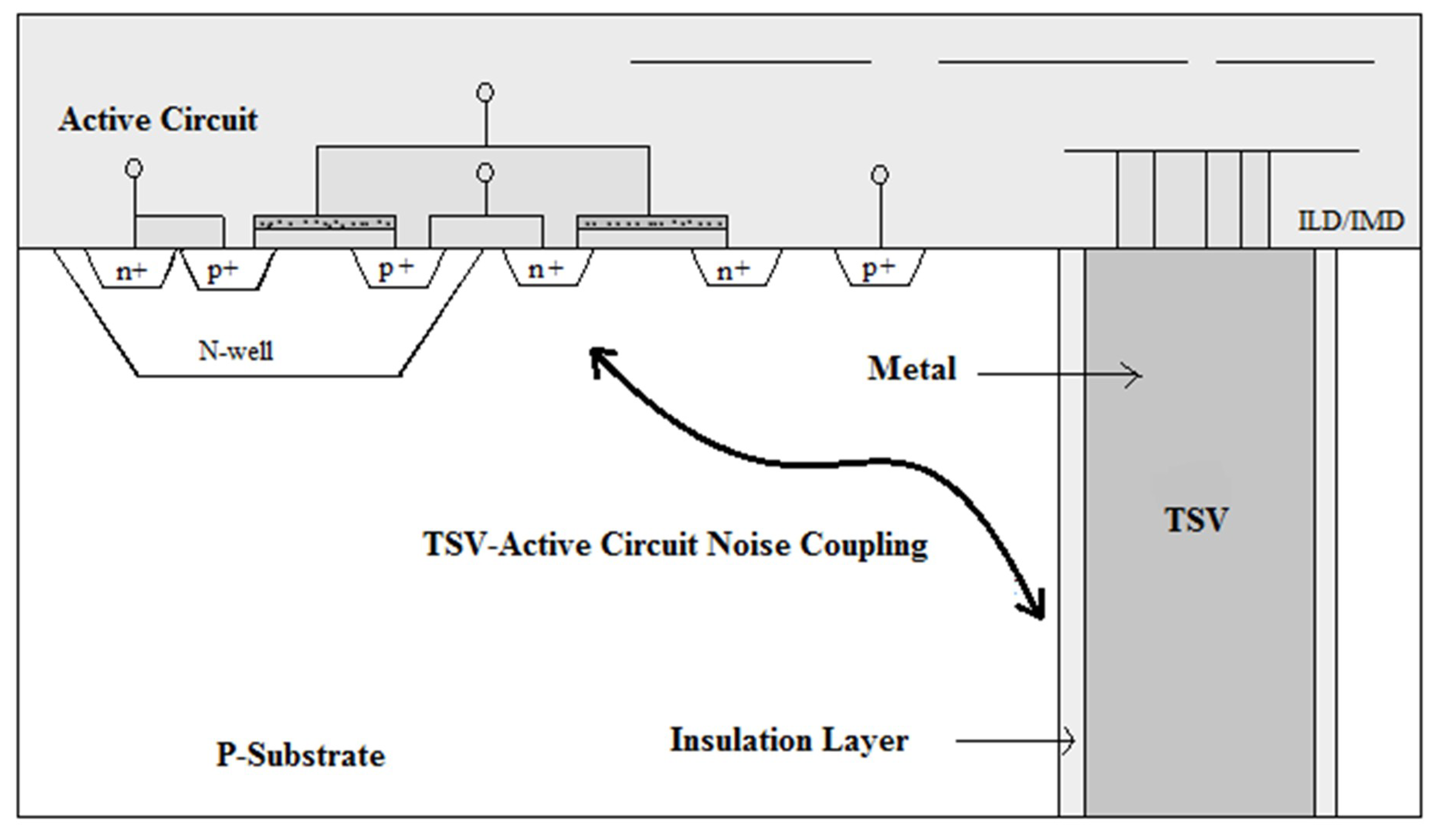
1. Introduction
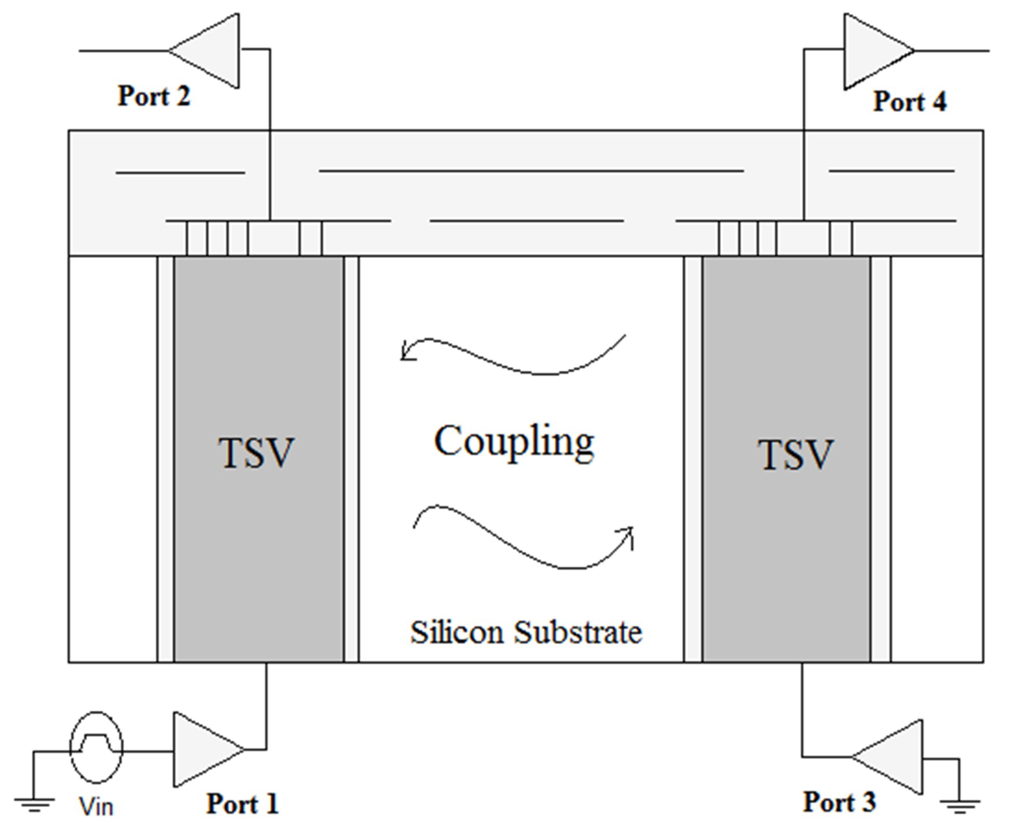
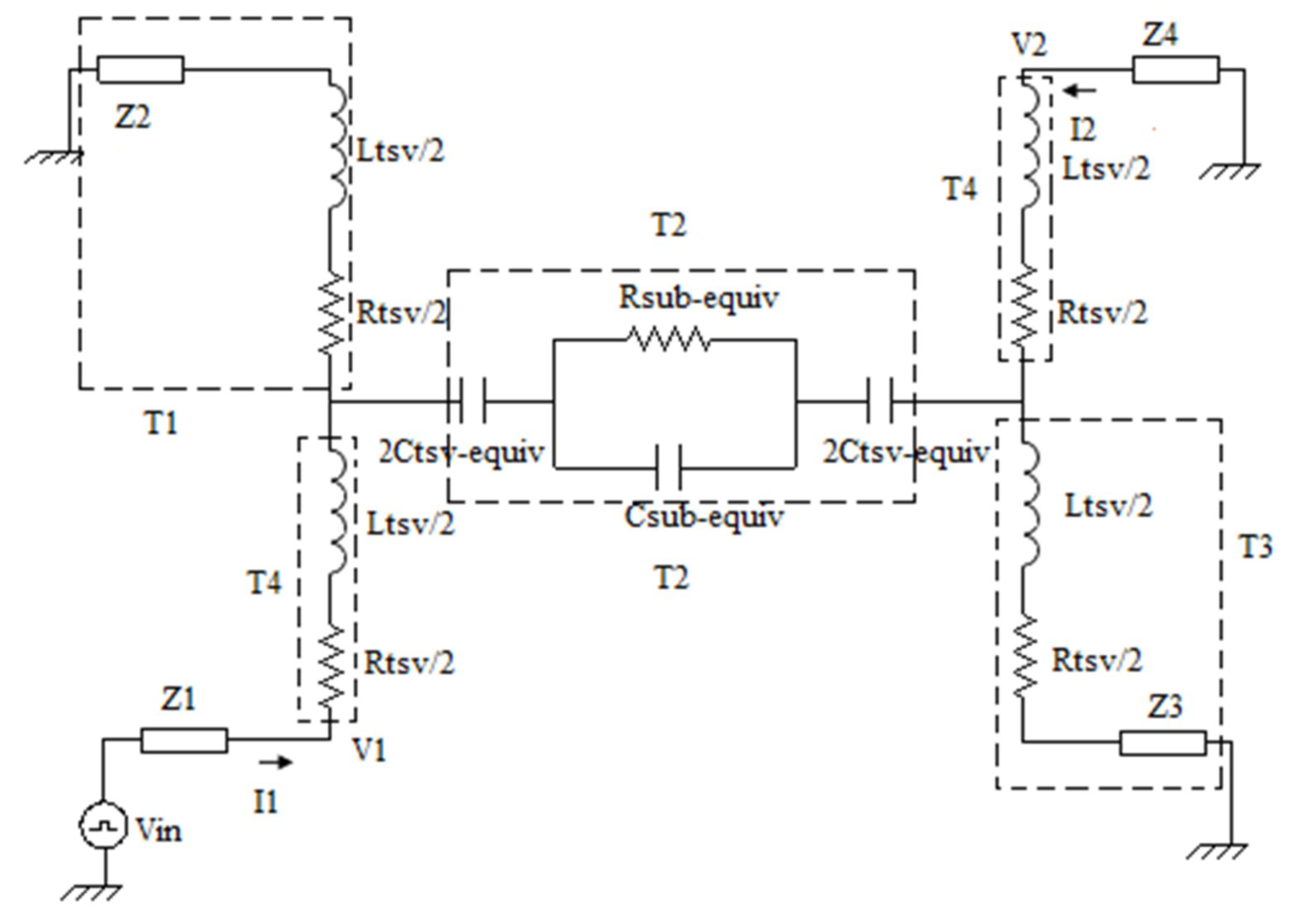
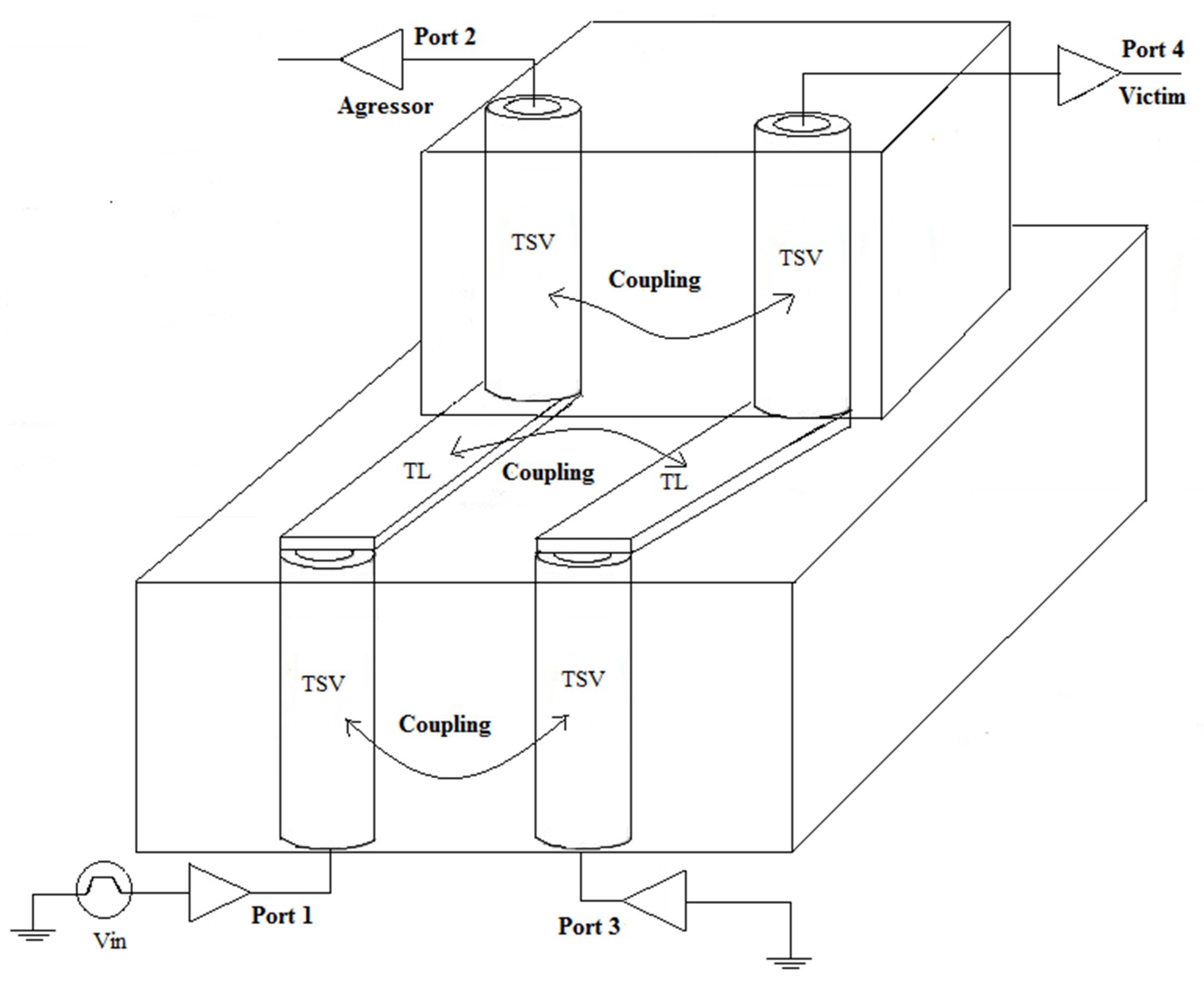
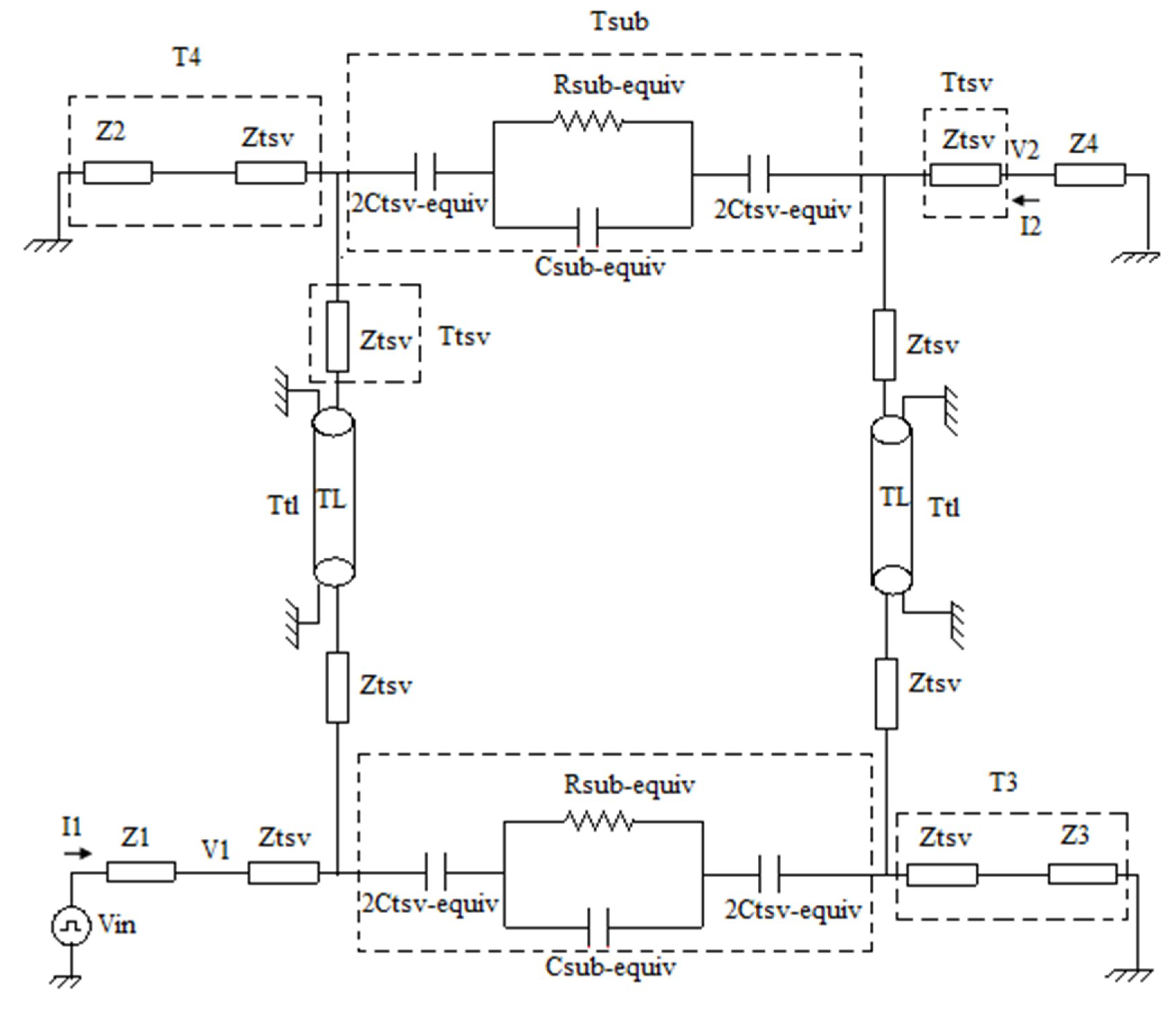
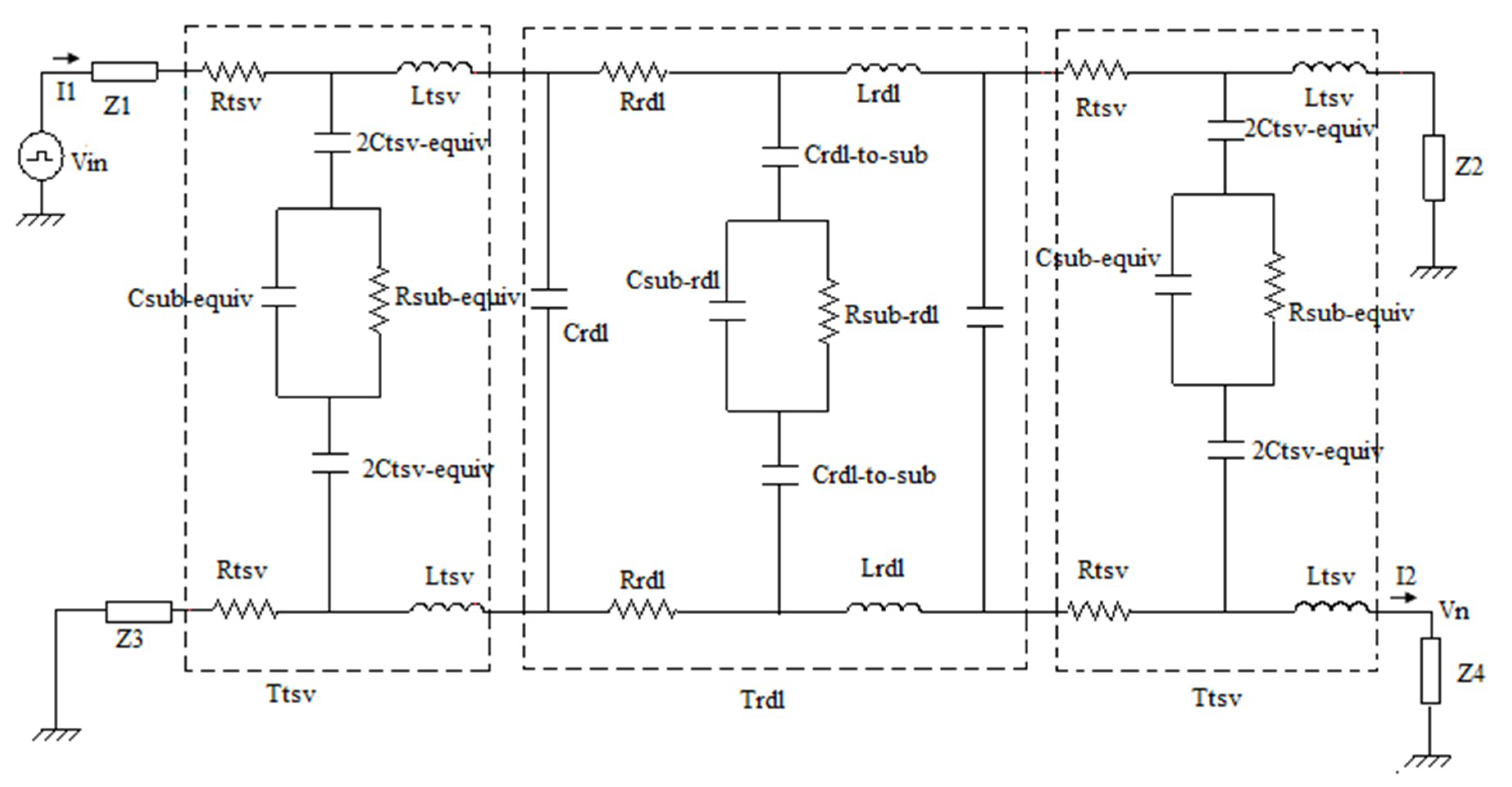
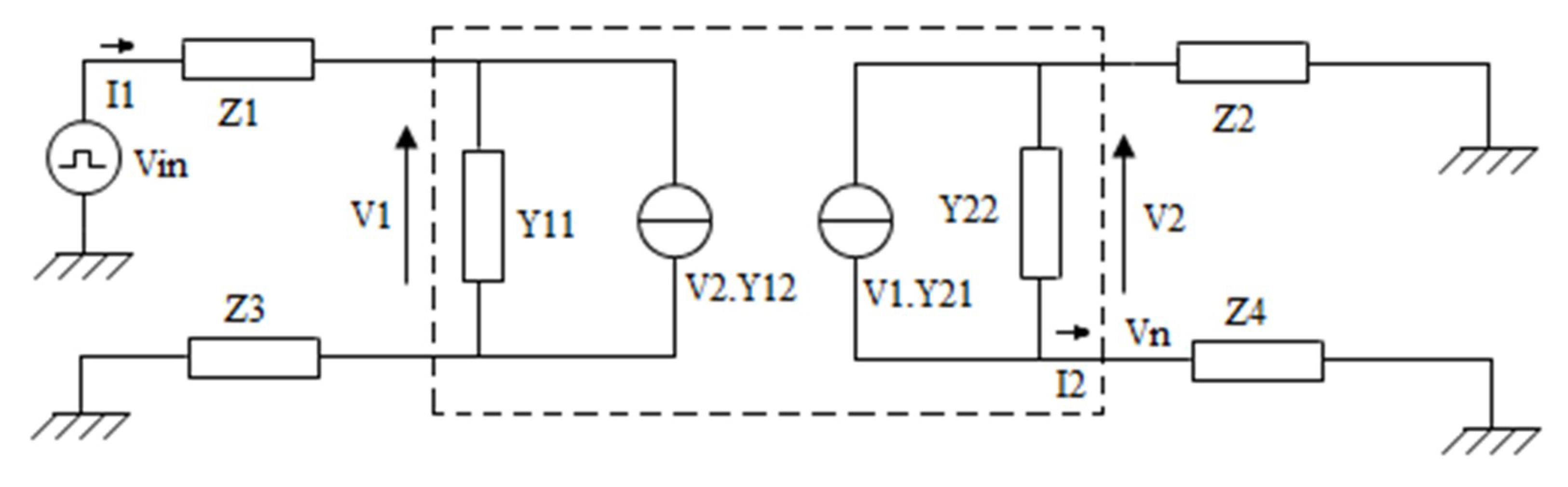
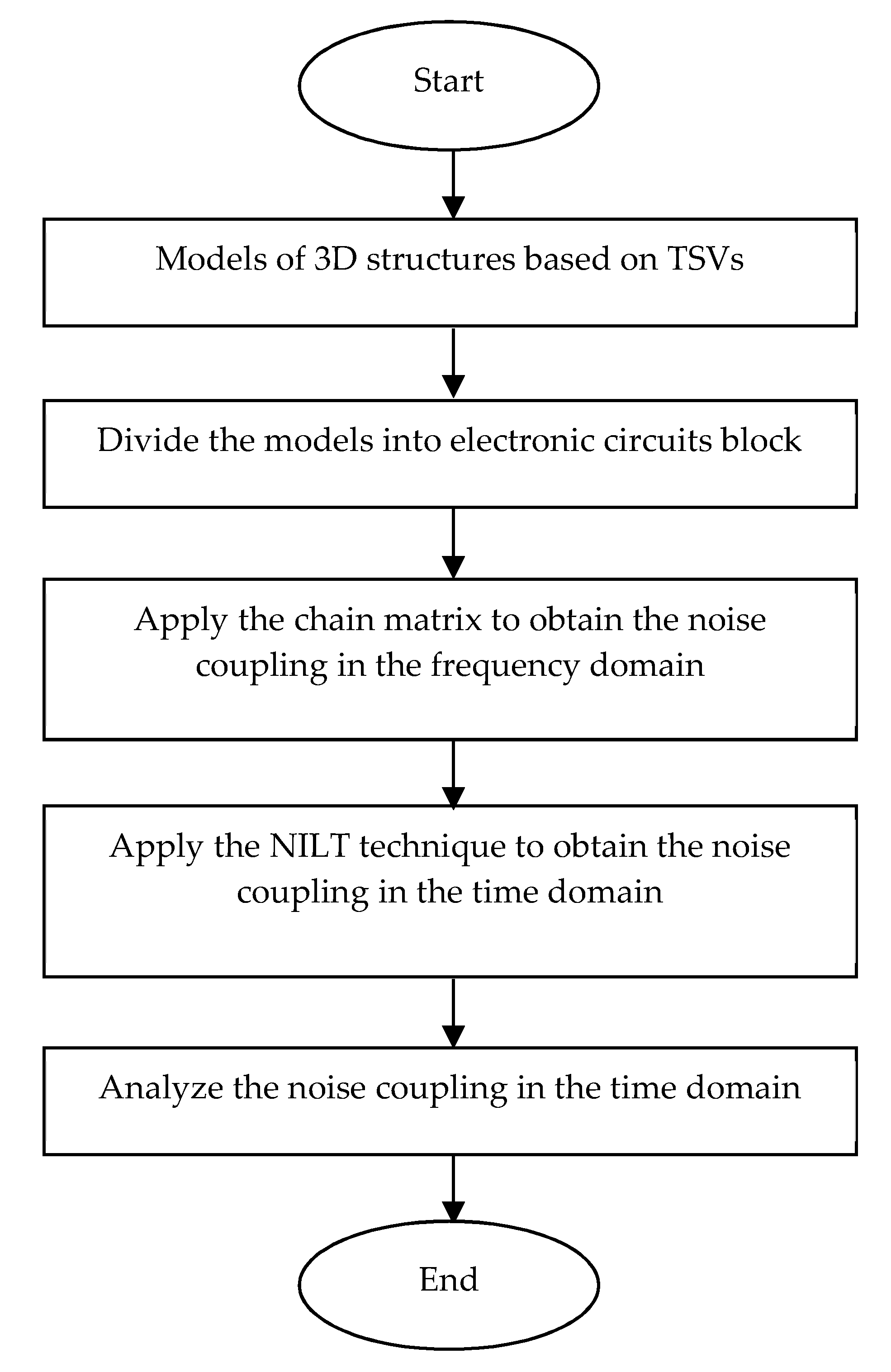
2. Calculation of Time-Domain TSV Noise Coupling in 3D-IC Design with NILT
3. Results and Discussions
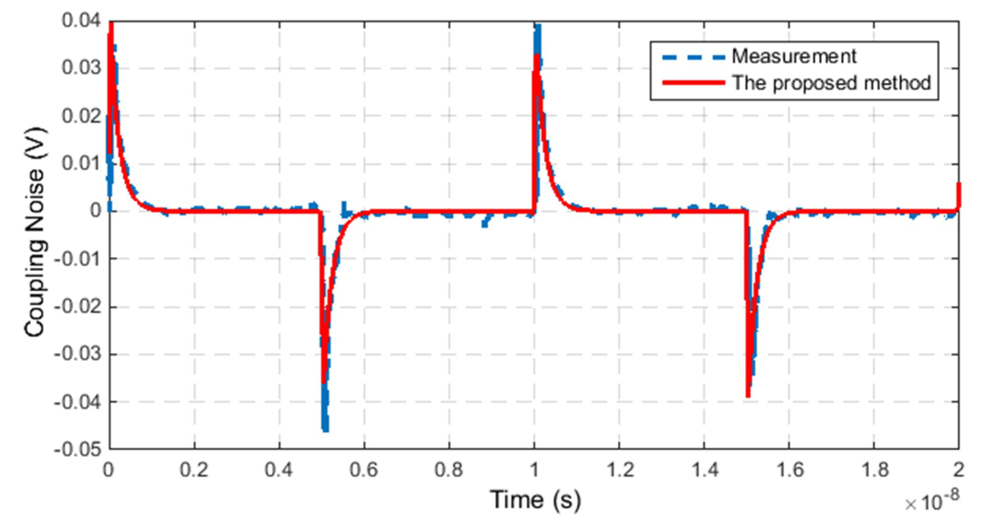
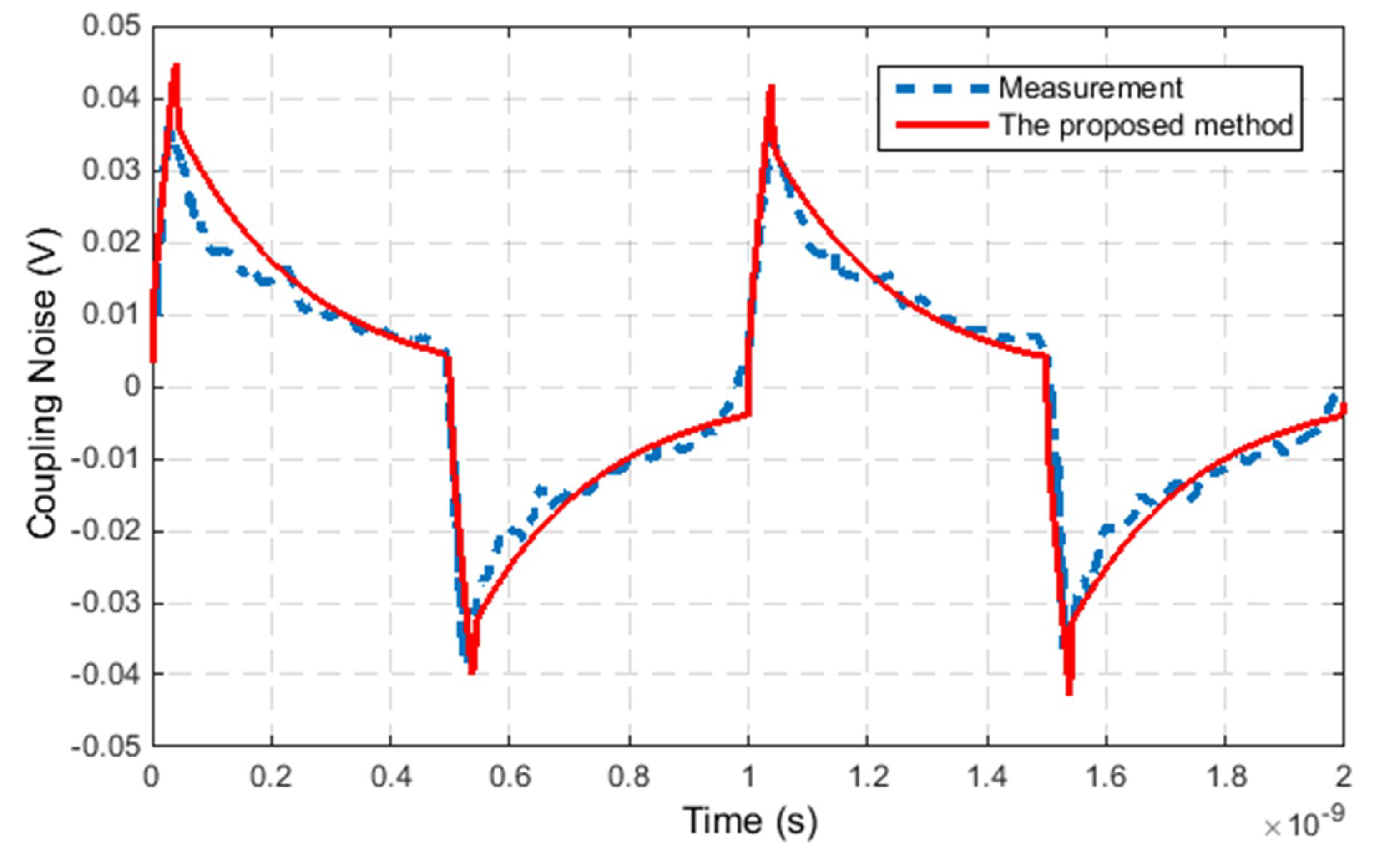
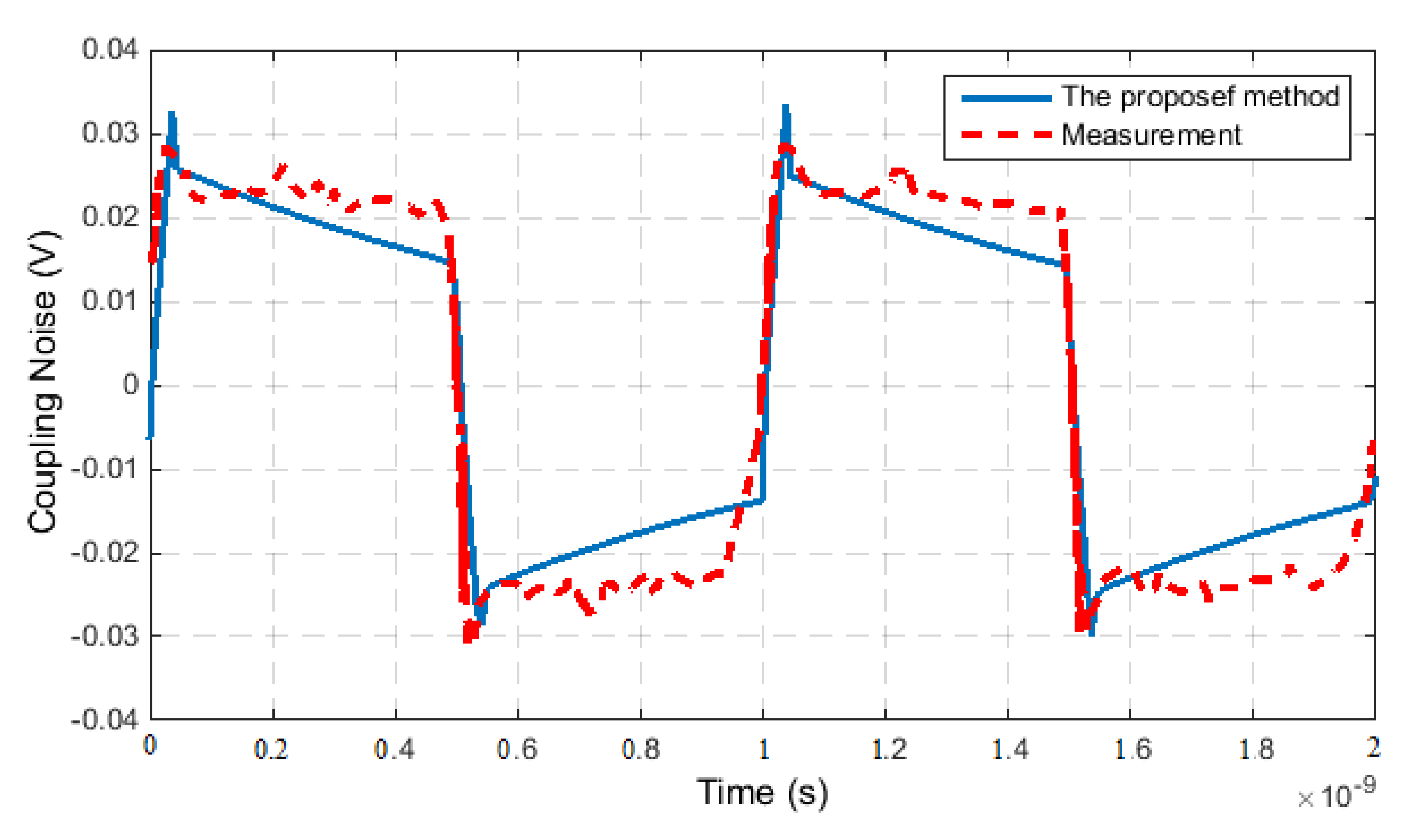
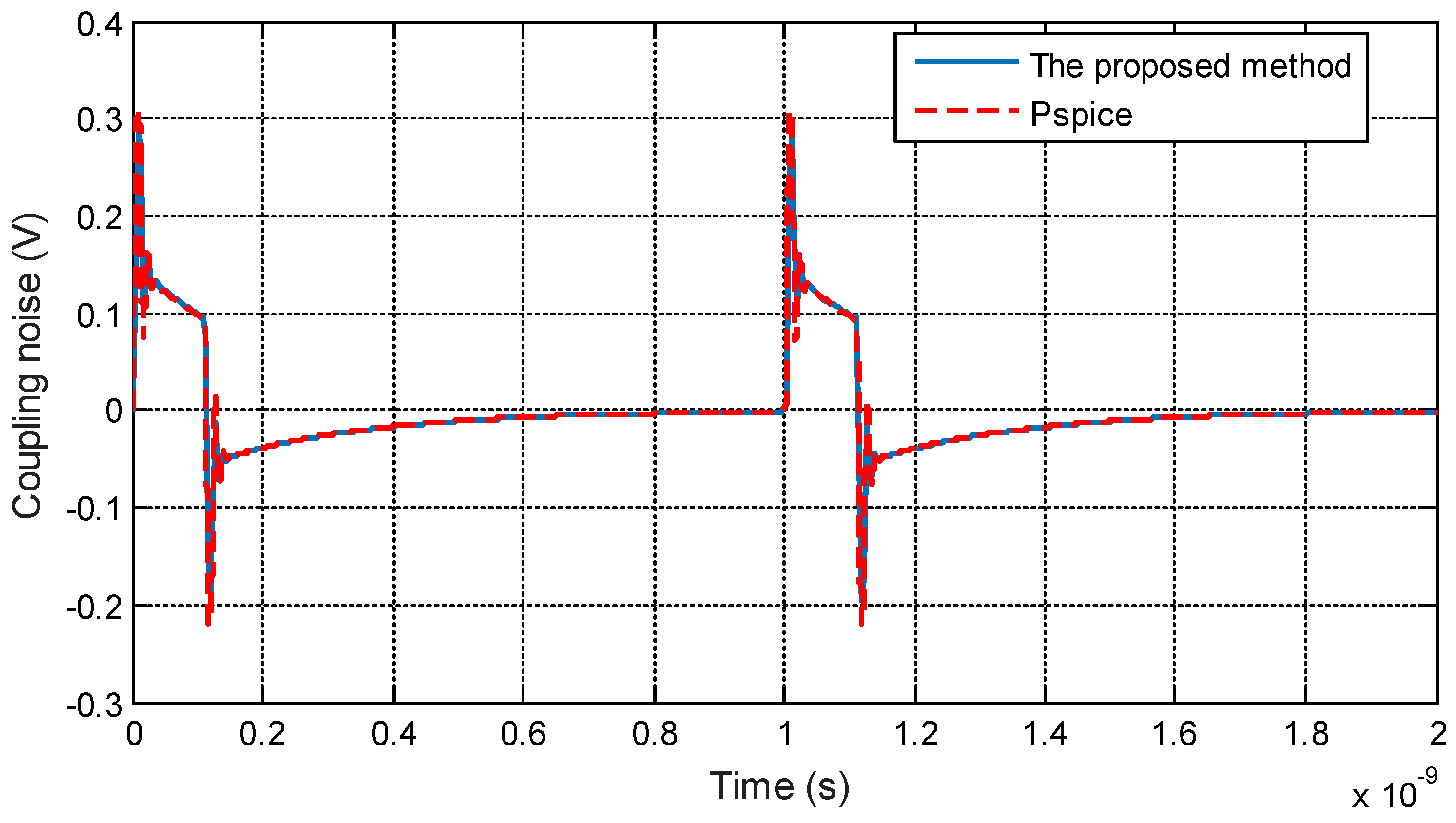
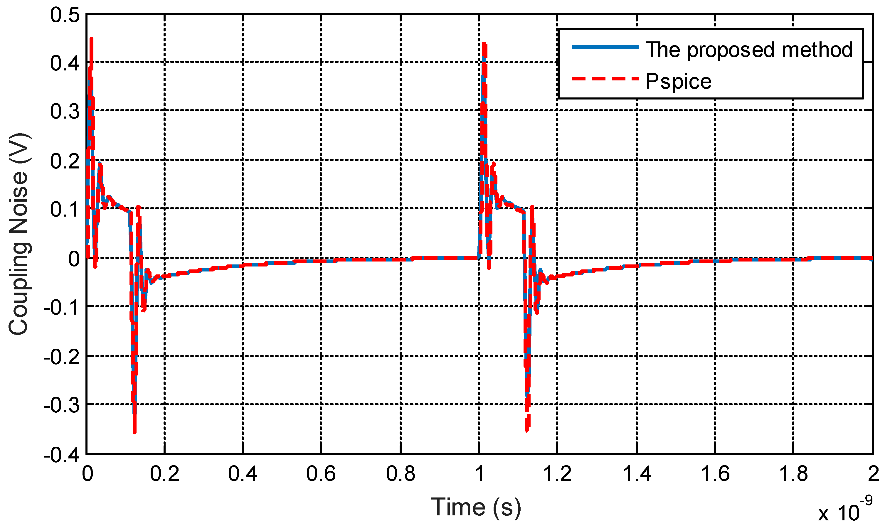
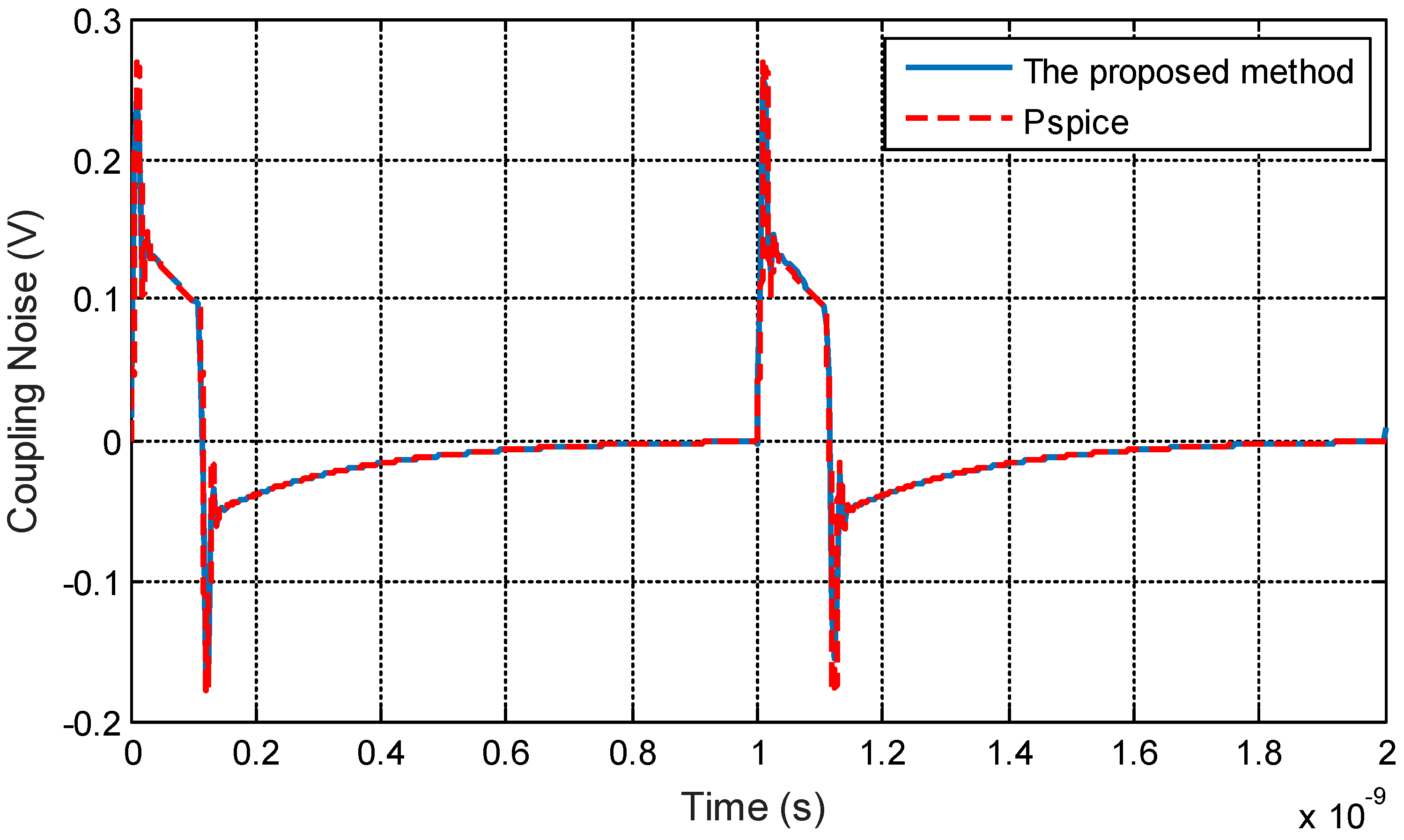
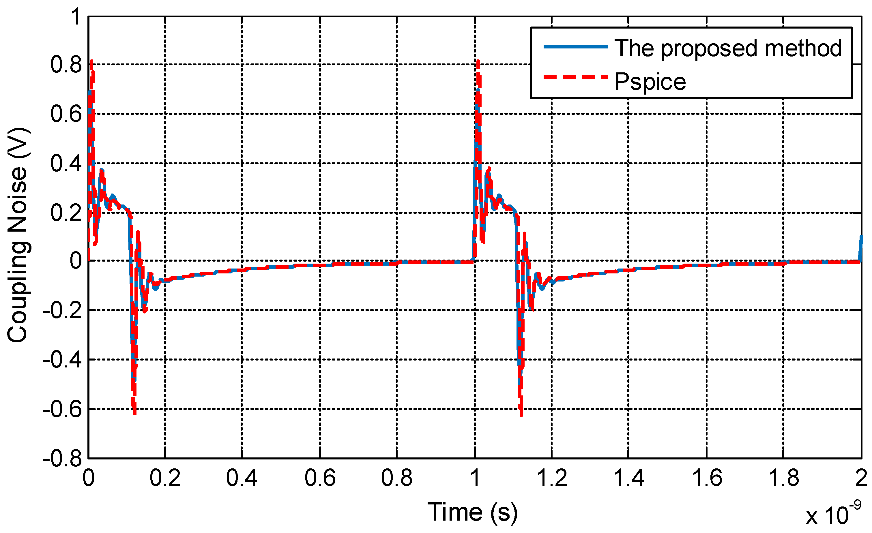
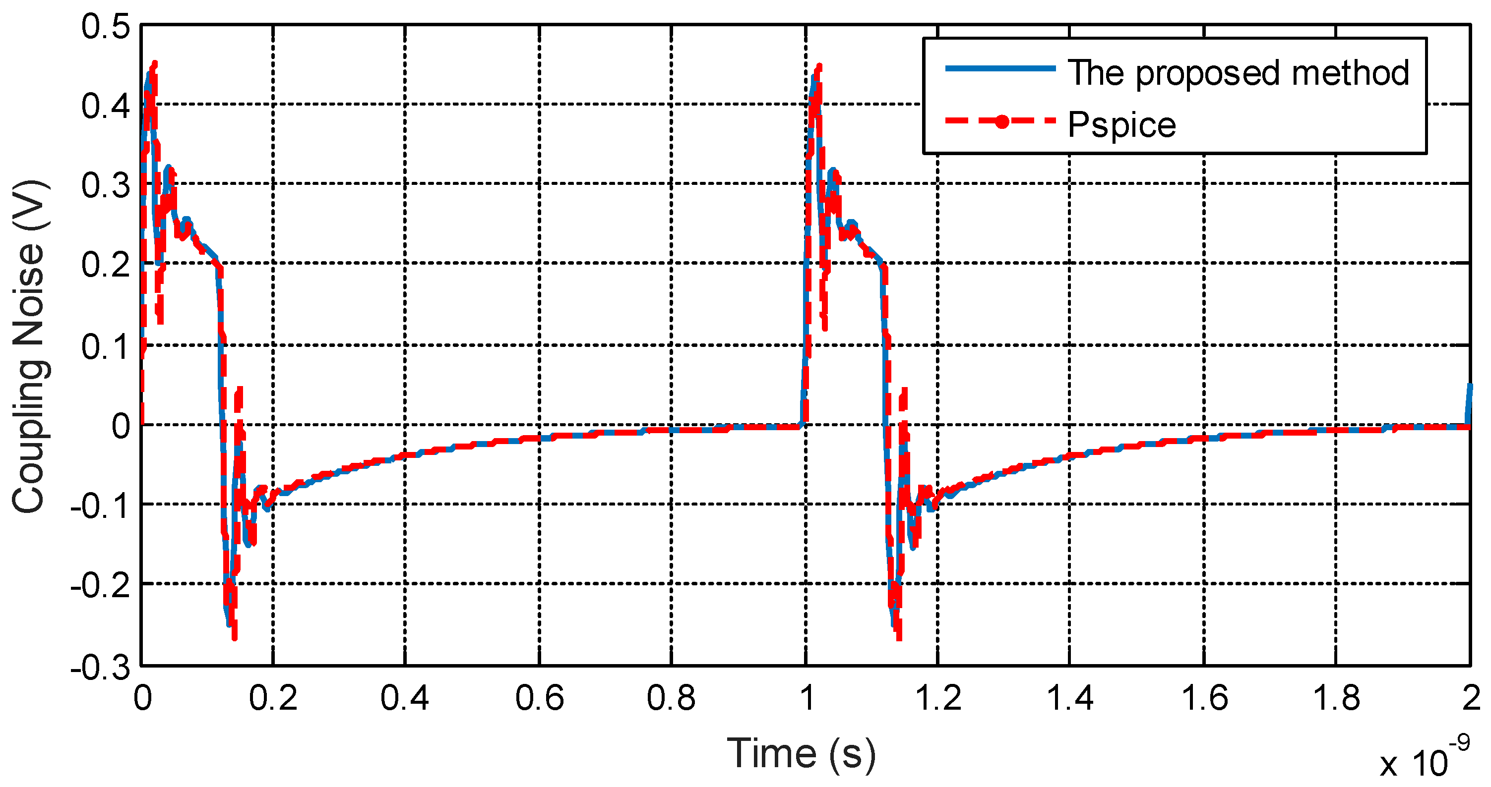
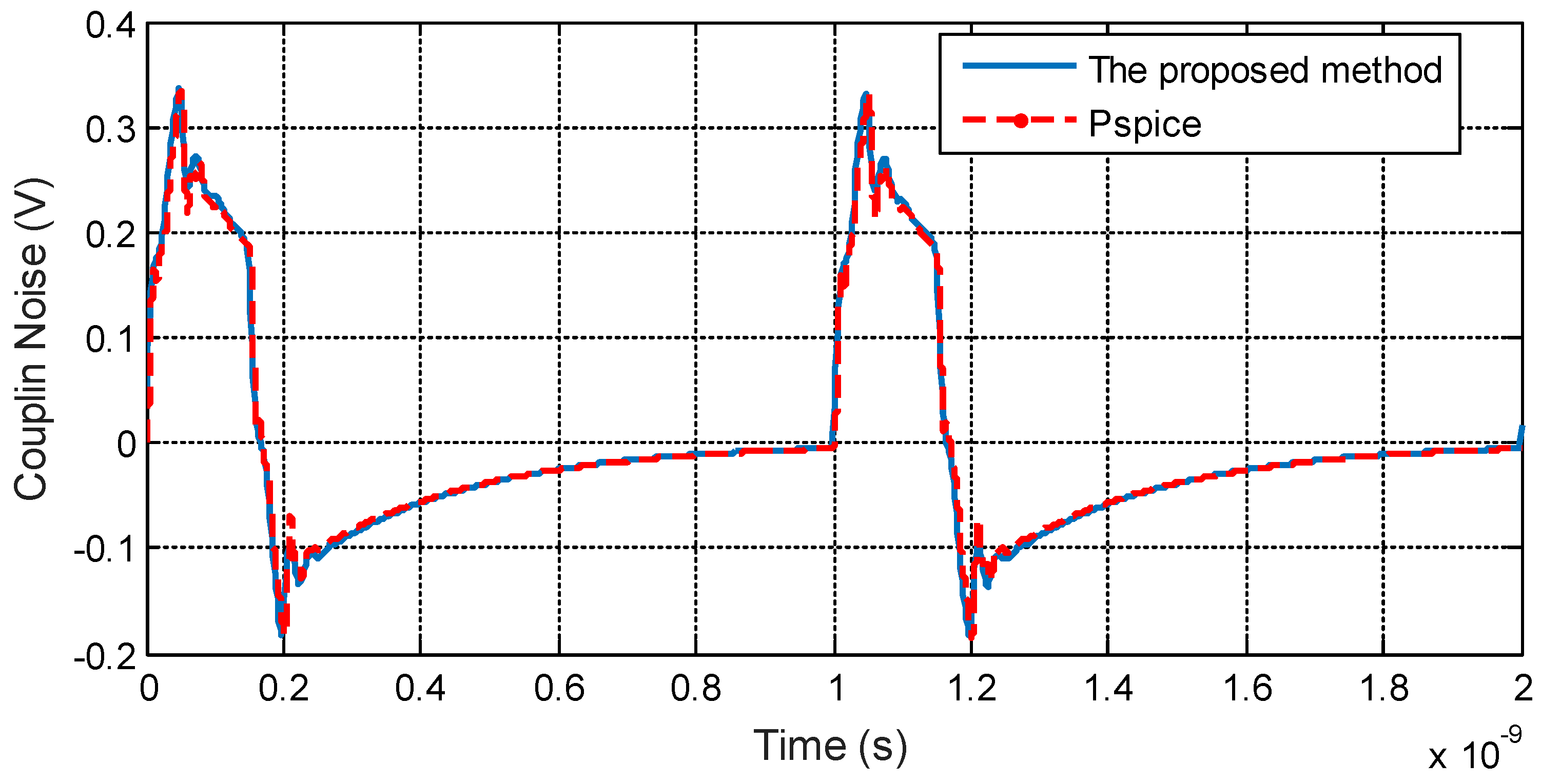
3.1. Validation of the Proposed Method
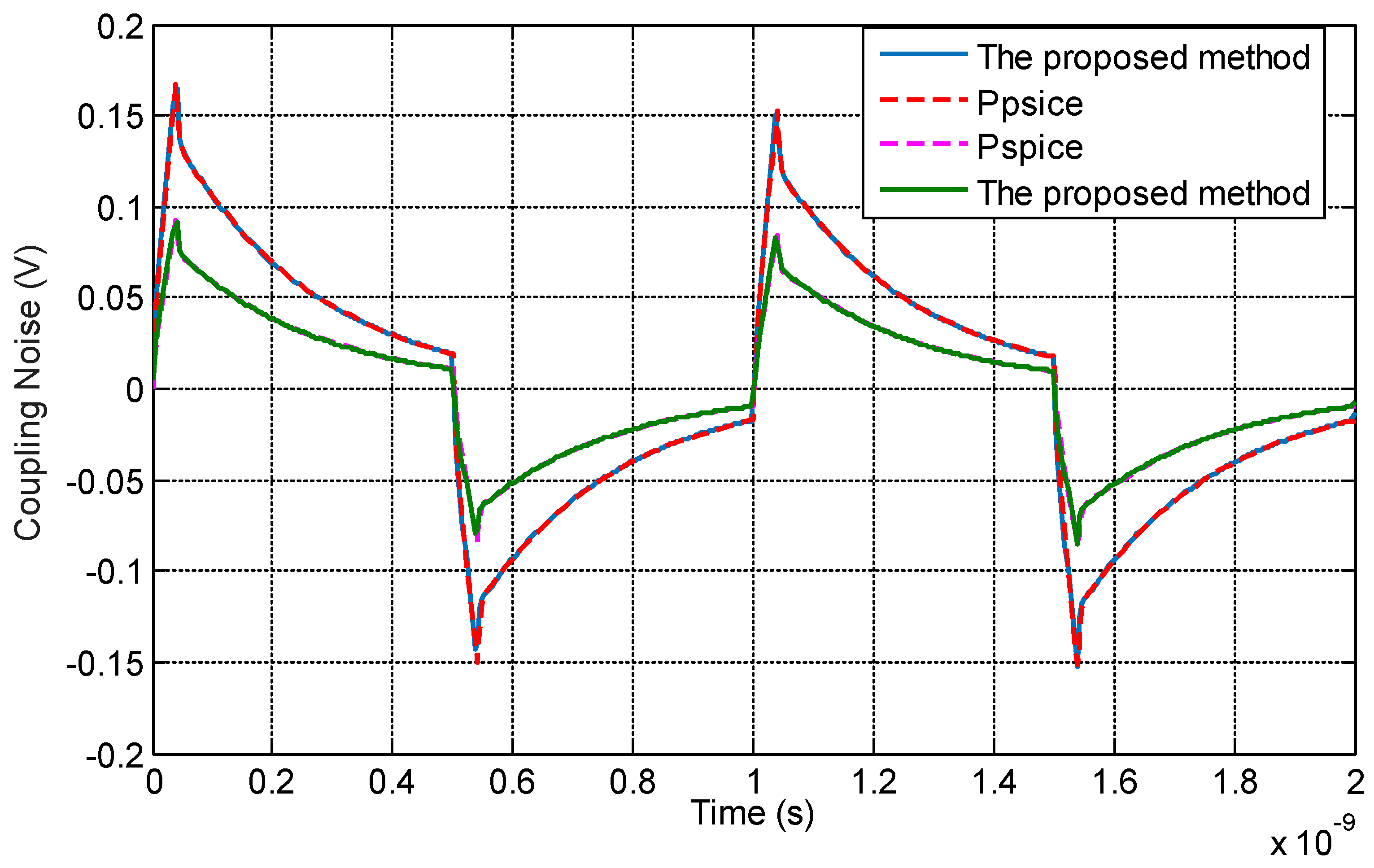
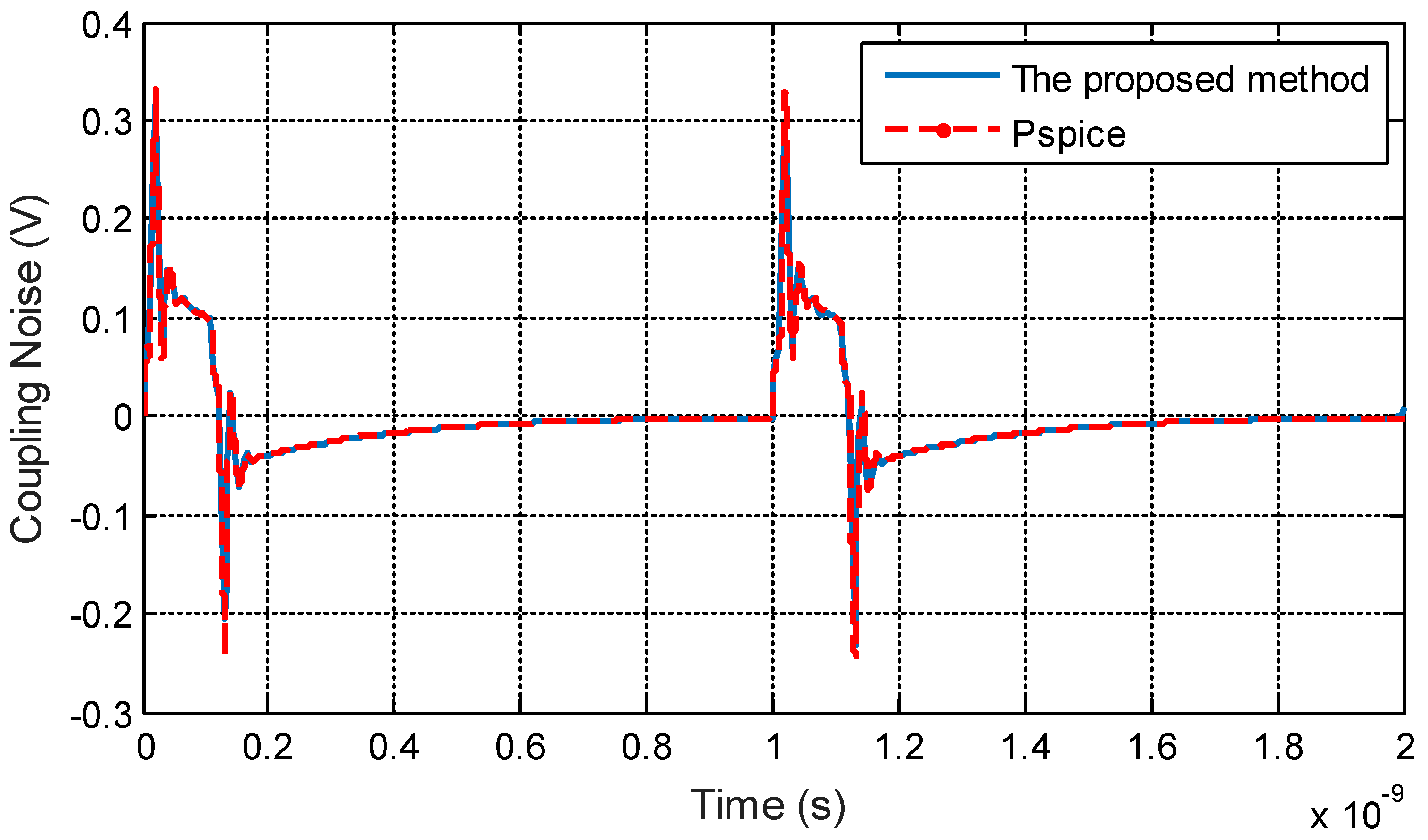
3.2. Time-Domain Analysis of the Coupling Noise with I/O Drivers Load
4. Conclusions
Author Contributions
Funding
Conflicts of Interest
References
- Meindl, J.D.; Chen, Q.; Davis, J.A. Limits on Silicon Nanoelectronics for Terascale Integration. Comput. Sci. 2001, 293, 2044–2049. [Google Scholar] [CrossRef] [PubMed]
- Borkar, S. Design Challenges of Technology Scaling. IEEE Micro. 1991, 19, 23–29. [Google Scholar] [CrossRef]
- Lee, M.; Pak, J.S.; Kim, J. Electrical Design of through Silicon Via; Springer: Dordrecht, The Netherlands; Heidelberg, Germany; New York, NY, USA; London, UK, 2014. [Google Scholar]
- Koester, S.J.; Young, A.M.; Yu, R.R.; Purushothaman, S.; Chen, K.-N.; La Tulipe, D.C.; Rana, N.; Shi, L.; Wordeman, M.R.; Sprogis, E.J. Wafer-level 3D integration technology. IBM J. Res. Dev. 2008, 52, 583–597. [Google Scholar] [CrossRef]
- Knicherbacker, J.U.; Andry, P.S.; Dang, B.; Horton, R.R.; Interrante, M.J.; Patel, C.S.; Polastre, R.J.; Sakuma, K.; Sirdeshmukh, R.; Sprogis, E.J.; et al. Three-dimensional silicon integration. IBM J. Res. Dev. 2008, 52, 553–569. [Google Scholar] [CrossRef]
- Garrou, P.E. Wafer-level 3D integration moving forward. Semicond. Int. 2006, 29, 12–17. [Google Scholar]
- Cadix, L.; Fuchs, C.; Rousseau, M.; LeDuc, P.; Chaabouni, H.; Thuaire, A.; Brocard, M.; Valentian, A.; Farcy, A.; Bermond, C.; et al. Integration and frequency dependent parametric modeling of Through Silicon Via involved in high density 3D chip stacking. ECS Trans. 2010, 33, 1–21. [Google Scholar]
- Ryu, C.; Lee, J.; Lee, H.; Lee, K.; Oh, T.; Kim, J. High Frequency Electrical Model of through Wafer Via for 3D Stacked Chip Packaging. In Proceedings of the ESTC, Dresden, Germany, 5–7 September 2006; pp. 215–220. [Google Scholar]
- Bandyopadhyay, T.; Han, K.J.; Chung, D.; Chatterjee, R.; Swaminathan, M.; Tummala, R. Rigorous Electrical Modeling of TSVs with MOS Capacitance Effects. IEEE Trans. Compon. Packag. Manuf. Technol. 2011, 1, 893–903. [Google Scholar] [CrossRef]
- Liu, E.X.; Li, E.P.; Ewe, W.B.; Lee, H.M.; Lim, T.G.; Gao, S. Compact Wideband Equivalent Circuit Model for Electrical Modeling of TSV. IEEE Trans. Microw. Theory Tech. 2011, 59, 1454–1460. [Google Scholar]
- Katti, G.; Stucchi, M.; Meyer, K.D.; Dehaene, W. Electrical Modeling and Characterization of TSV for 3D-ICs. IEEE Trans. Electron Devices 2010, 57, 256–262. [Google Scholar] [CrossRef]
- Xu, C.; Kourkoulos, V.; Suaya, R.; Banerjee, K. A Fully Analytical Model for the Series Impedance of TSV with Consideration of Substrate Effects and Coupling with Horizontal Interconnects. IEEE Trans. Electron Devices 2011, 58, 3529–3540. [Google Scholar] [CrossRef]
- Cho, J.; Song, E.; Yoon, K.; Pak, J.S.; Kim, J.; Lee, W.; Song, T.; Kim, K.; Lee, J.; Lee, H.; et al. Modeling and Analysis of TSV Noise Coupling and Suppressing Using a Guard Ring. IEEE Trans. Compon. Packag. Manuf. Technol. 2011, 1, 220–233. [Google Scholar] [CrossRef]
- Lim, J.; Cho, J.; Jung, D.H.; Kim, J.J.; Choi, S.; Kim, D.H.; Lee, M.; Kim, J. Modeling and analysis of TSV noise coupling effects on RFLC-VCO and shielding structures in 3D-IC. IEEE Trans. Electromagn. Compat. 2018, 60, 1939–1947. [Google Scholar] [CrossRef]
- Rimolo-Donadio, R.; Gu, X.; Kwark, Y.; Ritter, M.; Archambeault, B.; De Paulis, F.; Zhang, Y.; Fan, J.; Bruns, H.-D.; Schuster, C. Physics-based via and trace models for efficient link simulation on multilayer structures up to 40 GHz. IEEE Trans. Microw. Theory Tech. 2009, 57, 2072–2083. [Google Scholar] [CrossRef]
- Han, K.J.; Swaminathan, M.; Bandyopadhyay, T. Electromagnetic modeling of through-silicon via (TSV) interconnections using cylindrical modal basis functions. IEEE Trans. Adv. Packag. 2010, 33, 804–817. [Google Scholar] [CrossRef]
- Beanato, G.; Gharibdoust, K.; Cevrero, A.; De Micheli, G.; Leblebici, Y. Design and analysis of jitter-aware low-power and high-speed TSV link for 3D-ICs. Microelectron. J. 2016, 48, 50–59. [Google Scholar] [CrossRef]
- Attarzadeh, H.; Lim, S.K.; Ytterdal, T. Design and Analysis of a Stochastic Flash Analog-to-Digital Converter in 3D-IC technology for integration with ultrasound transducer array. Microelectron. J. 2016, 48, 39–49. [Google Scholar] [CrossRef]
- Bamberg, L.; Najafi, A.; García-Ortiz, A. Edge effects on the TSV array capacitances and their performance influence. Integration 2018, 61, 1–10. [Google Scholar] [CrossRef]
- Xu, C.; Li, H.; Suaya, R.; Banerjee, K. Compact AC modeling and performance analysis of through-silicon vias in 3D-ICs. IEEE Trans. Electron. Devices 2010, 57, 3405–3417. [Google Scholar] [CrossRef]
- Kim, J.; Pak, J.S.; Cho, J.; Song, E.; Cho, J.; Kim, H.; Song, T.; Lee, J.; Lee, H.; Park, K.; et al. High-Frequency scalable electrical model and analysis of Through Silicon Via (TSV). IEEE Trans. Compon. Packag. Manuf. Technol. 2011, 1, 181–195. [Google Scholar]
- Kerns, K.J.; Wemple, I.L.; Yang, A.T. Stable and efficient reduction of substrate model networks using congruence transforms. In Proceedings of the IEEE/ACM International Conference Computer-Aided Design, San Jose, CA, USA, 5–9 November 1995; pp. 207–214. [Google Scholar]
- Verghese, N.K.; Allstot, D.J.; Masui, S. Rapid simulation of substrate coupling effects in mixed-mode ICs. In Proceedings of the IEEE Custom Integrated Circuits Conference, San Diego, CA, USA, 9–12 May 1993; pp. 18.3.1–18.3.4. [Google Scholar]
- Shim, Y.; Park, J.; Kim, J.; Song, E.; Yoo, J.; Pak, J.; Kim, J. Modeling and analysis of simultaneous switching noise coupling for a CMOS negative-feedback operational amplifier in system-in-package. IEEE Trans. Electromagn. Compat. 2009, 51, 763–773. [Google Scholar] [CrossRef]
- Koo, K.; Shim, Y.; Yoon, C.; Kim, J.; Yoo, J.; Pak, J.S.; Kim, J. Modeling and analysis of power supply noise imbalance on ultra-high frequency differential low noise amplifiers in a system-in-package. IEEE Trans. Adv. Packag. 2010, 33, 602–616. [Google Scholar] [CrossRef]
- Li, J.; Farquharson, C.G.; Hu, X. Three effective inverse Laplace transform algorithms for computing time-domain electromagnetic responses. Geophysics 2016, 81, E113–E128. [Google Scholar] [CrossRef]
- Liu, L.; Xue, D.; Zhang, S. Closed-loop time response analysis of irrational fractional-order systems with numerical Laplace transform technique. Appl. Math. Comput. 2019, 350, 133–152. [Google Scholar] [CrossRef]
- Wan, Q.; Zhan, H. On different numerical inverse Laplace methods for solute transport. Adv. Water Resour. 2015, 75, 80–92. [Google Scholar]
- Dingfelder, B.; Weideman, J.A.C. An improved Talbot method for numerical Laplace transform inversion. Numer. Algorithms 2015, 68, 167–183. [Google Scholar] [CrossRef]
- Brancik, L. Numerical Inversion of Two-Dimensional Laplace Transforms Based on Partial Inversions. In Proceedings of the 17th international Conference Radioelektronika, Brno, Czech Republic, 24–25 April 2007. [Google Scholar]
- Brancik, L. Technique of 3D NILT based on complex Fourier Series and Quotient-Difference Algorithms. In Proceedings of the 17th IEEE International Conference on Electronics Circuits and Systems, Athens, Greece, 12–15 December 2010. [Google Scholar]
- Brancik, L. Matlab Simulation of Nonlinear Electrical Networks via Volterra Series Expansion and Multidimensional NILT. In Proceedings of the 2017 Progress in Electromagnetic Research Symposium-Fall, Singapore, 19–22 November 2017. [Google Scholar]
- Chakarothai, J. Novel FDTD Scheme for Analysis of Frequency-Dependent Medium Using Fast Inverse Laplace Transform and Prony’s Method. IEEE Trans. Antennas Propag. 2018. [Google Scholar] [CrossRef]
- Sheng, H.; Li, Y.; Chen, Y. Application of numerical inverse Laplace transform algorithms in fractional calculus. J. Frankl. Inst. 2011, 348, 315–330. [Google Scholar] [CrossRef]
- Brancik, L. Error Analysis at Numerical Inversion of Multidimensional Laplace Transforms Based on Complex Fourier Series Approximation. IEICE Trans. Fundam. Electron. Commun. Comput. Sci. 2011, E94-A, 999–1001. [Google Scholar] [CrossRef]
- Al-Zubaidi, N.; Brančík, L. Convergence Acceleration Techniques for Proposed Numerical Inverse Laplace Transform Method. In Proceedings of the 24th Telecommunication form TELFOR, Belgrade, Serbia, 22–23 November 2016. [Google Scholar]
- Ait-Belaid, K.; Belahrach, H.; Ayad, H. Investigation and Analysis of the Simultaneous Switching Noise in Power Distribution Network with Multi-Power Supplies of High-Speed CMOS Circuits. Act. Passiv. Electron. Compon. 2017. [Google Scholar] [CrossRef]


| Component | Value |
|---|---|
| Ctsv-equi | 201.3 fF |
| Rtsv | 0.001 Ω |
| Ltsv | 20.7 pH |
| Rsub-equi | 928.5 Ω |
| Csub-equiv | 11.2 fF |
| Component | Value |
|---|---|
| Ctsv-equiv | 817.5 fF |
| Rtsv | 0.001 Ω |
| Ltsv | 20.7 pH |
| Rsub-equiv | 879.5 Ω |
| Csub-equiv | 12 fF |
| Length of the Line | Component | Value |
|---|---|---|
| lRDL = 200 µm | Rrdl | 0.00672 Ω |
| Lrdl | 0.1664 nH | |
| Crdl | 7.66 fF | |
| Crdl-to-sub | 364.65 fF | |
| Csub-rdl | 0.13 fF | |
| Rsub-rdl | 836.12 fF | |
| lRDL = 500 µm | Rrdl | 0.0168 Ω |
| Lrdl | 0.42 nH | |
| Crdl | 19.15 fF | |
| Crdl-to-sub | 911.64 fF | |
| Csub-rdl | 0.33 fF | |
| Rsub-rdl | 334.44 Ω |
© 2019 by the authors. Licensee MDPI, Basel, Switzerland. This article is an open access article distributed under the terms and conditions of the Creative Commons Attribution (CC BY) license (http://creativecommons.org/licenses/by/4.0/).
Share and Cite
Ait Belaid, K.; Belahrach, H.; Ayad, H. Numerical Laplace Inversion Method for Through-Silicon Via (TSV) Noise Coupling in 3D-IC Design. Electronics 2019, 8, 1010. https://doi.org/10.3390/electronics8091010
Ait Belaid K, Belahrach H, Ayad H. Numerical Laplace Inversion Method for Through-Silicon Via (TSV) Noise Coupling in 3D-IC Design. Electronics. 2019; 8(9):1010. https://doi.org/10.3390/electronics8091010
Chicago/Turabian StyleAit Belaid, Khaoula, Hassan Belahrach, and Hassan Ayad. 2019. "Numerical Laplace Inversion Method for Through-Silicon Via (TSV) Noise Coupling in 3D-IC Design" Electronics 8, no. 9: 1010. https://doi.org/10.3390/electronics8091010
APA StyleAit Belaid, K., Belahrach, H., & Ayad, H. (2019). Numerical Laplace Inversion Method for Through-Silicon Via (TSV) Noise Coupling in 3D-IC Design. Electronics, 8(9), 1010. https://doi.org/10.3390/electronics8091010