Magnetic-Free Nonreciprocal Multifunction Device Based on Switched Delay Lines

Abstract
:1. Introduction
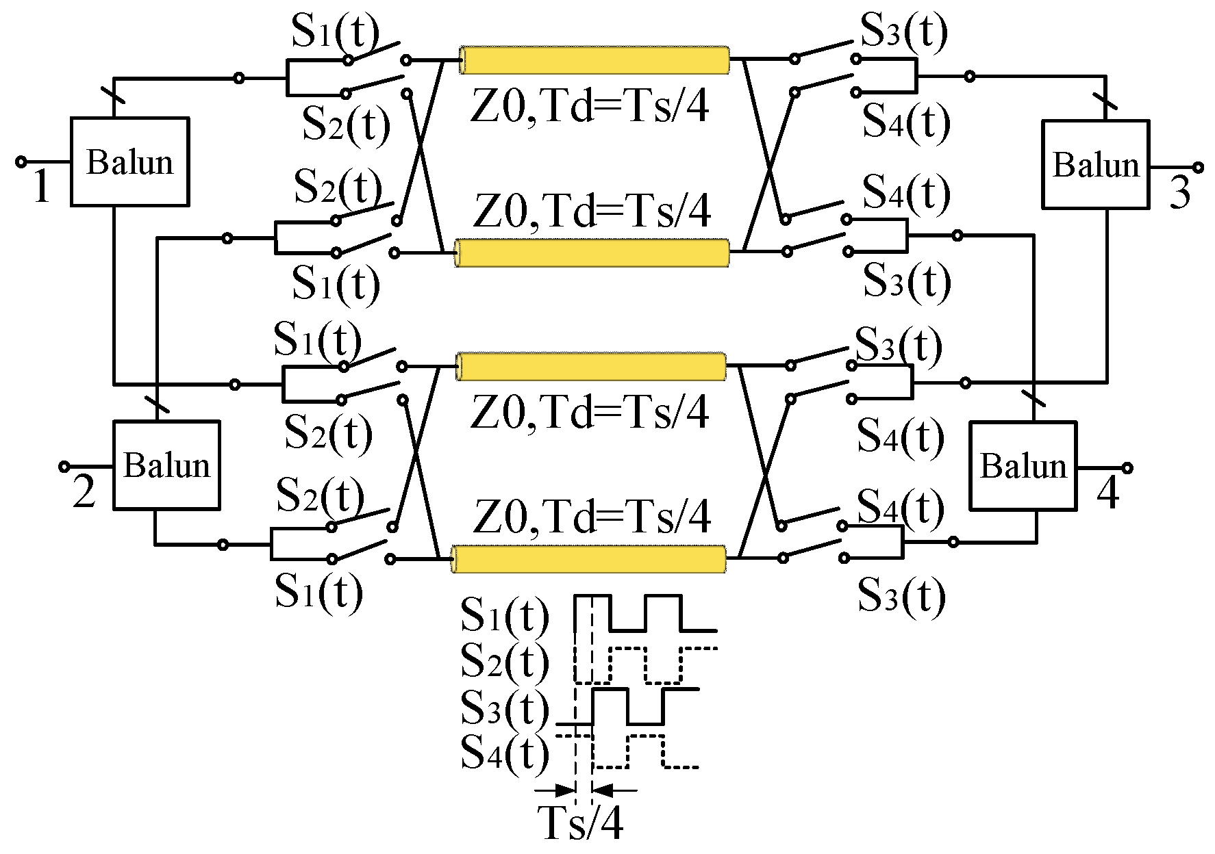
2. Principle of the Device
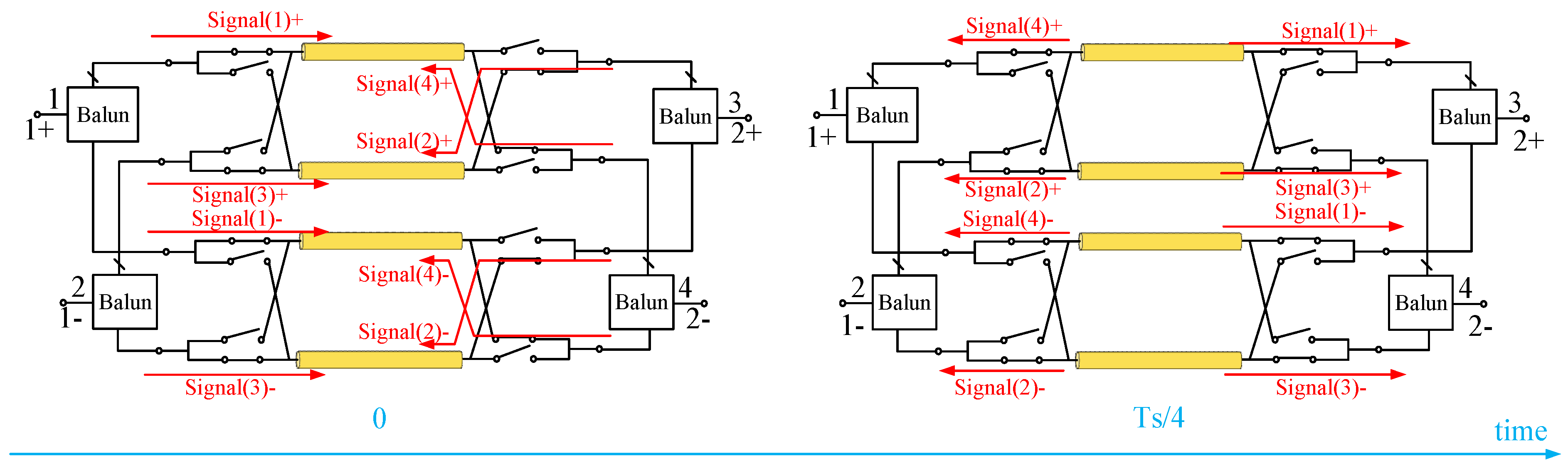
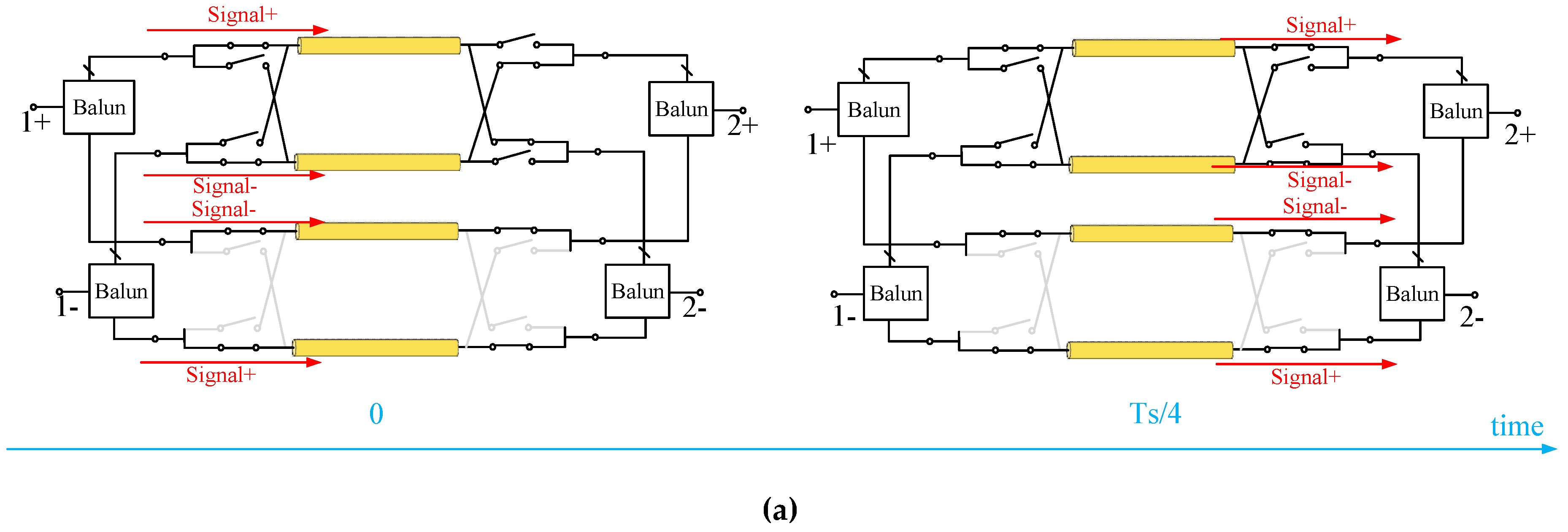
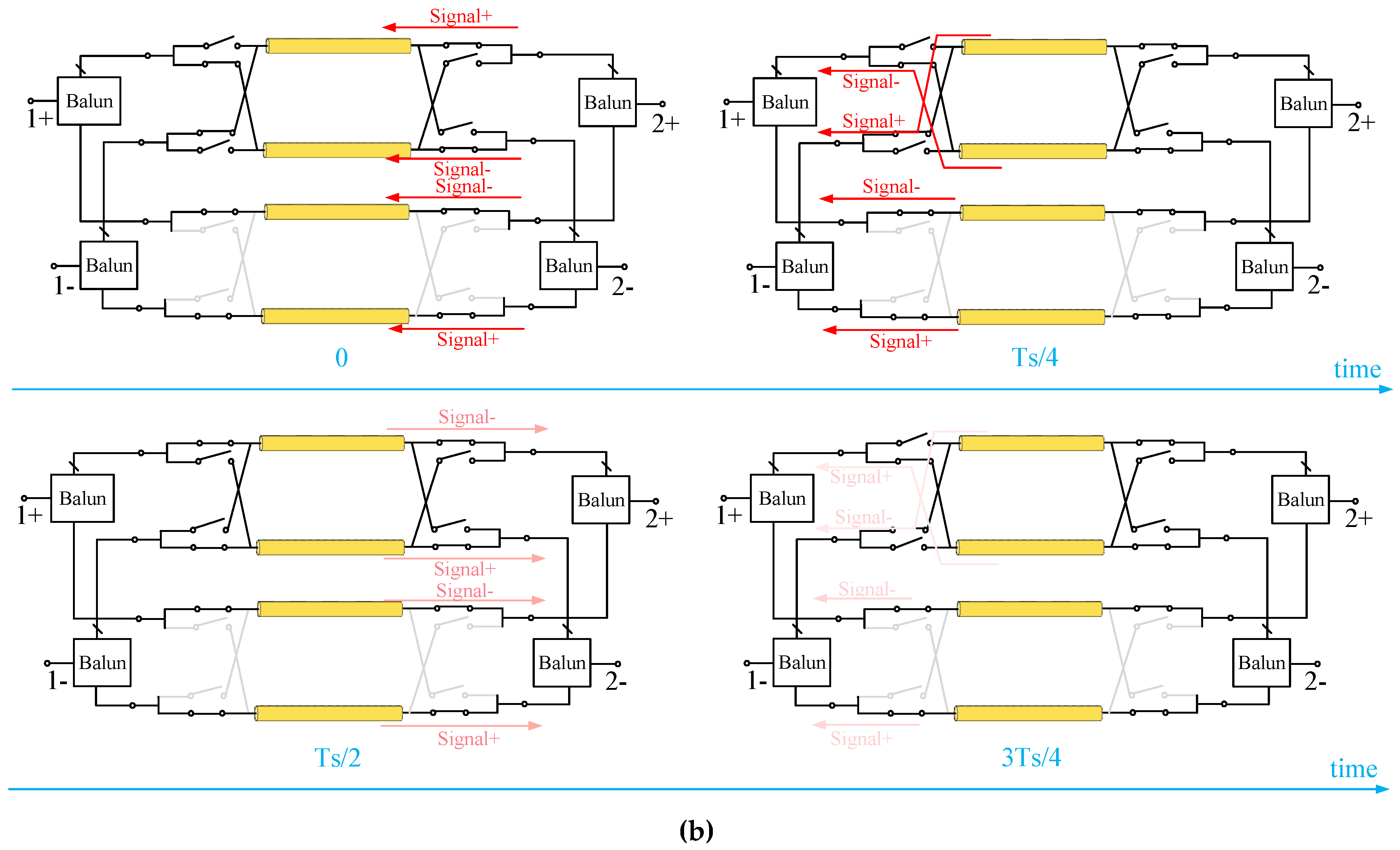
2.1. Gyrator
2.2. Circulator
2.3. Isolator
3. Simulation Verification of the Device
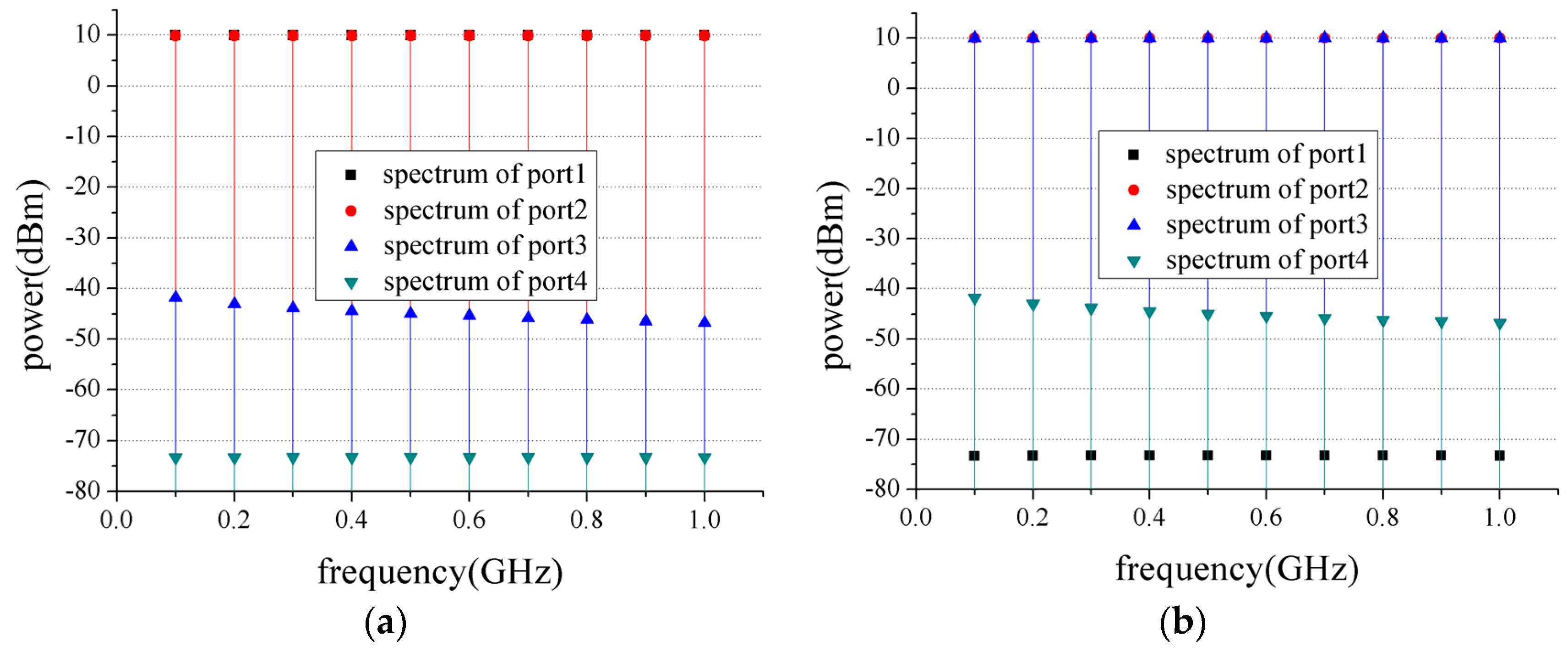
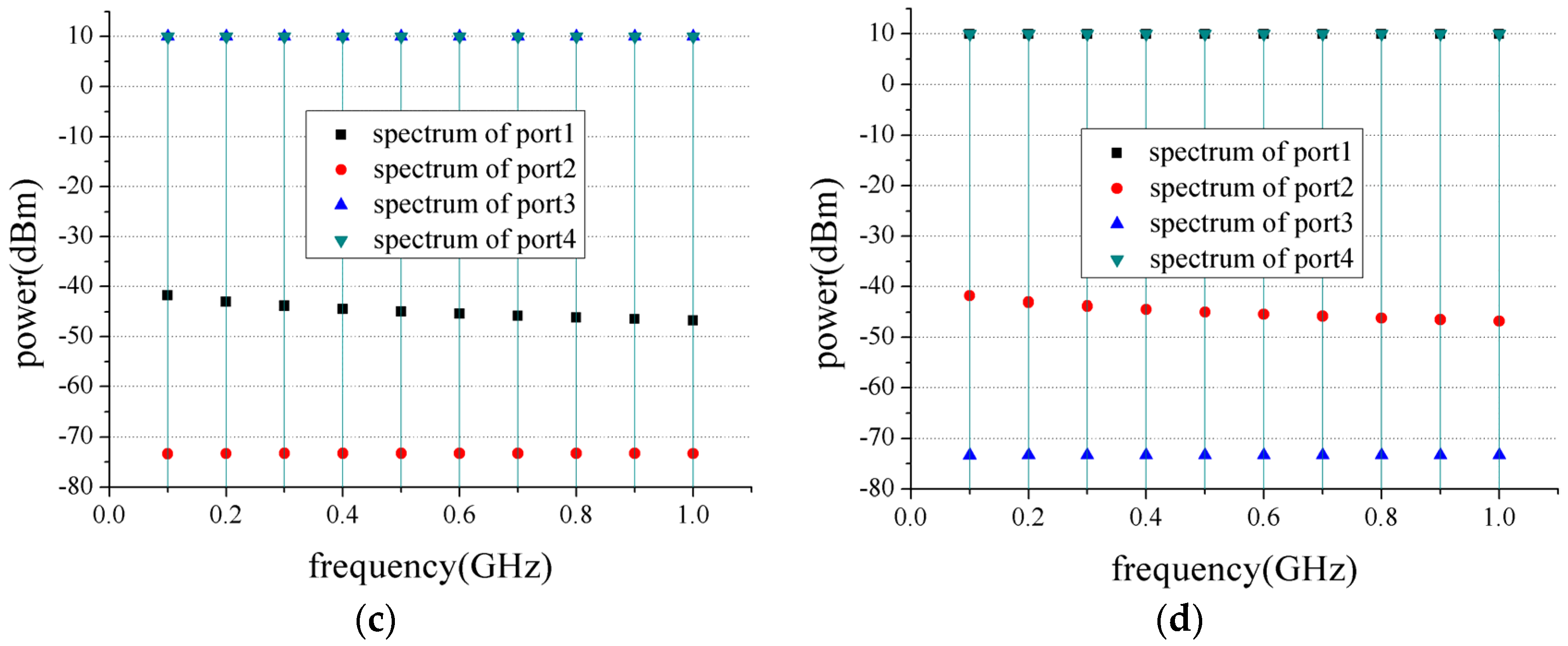
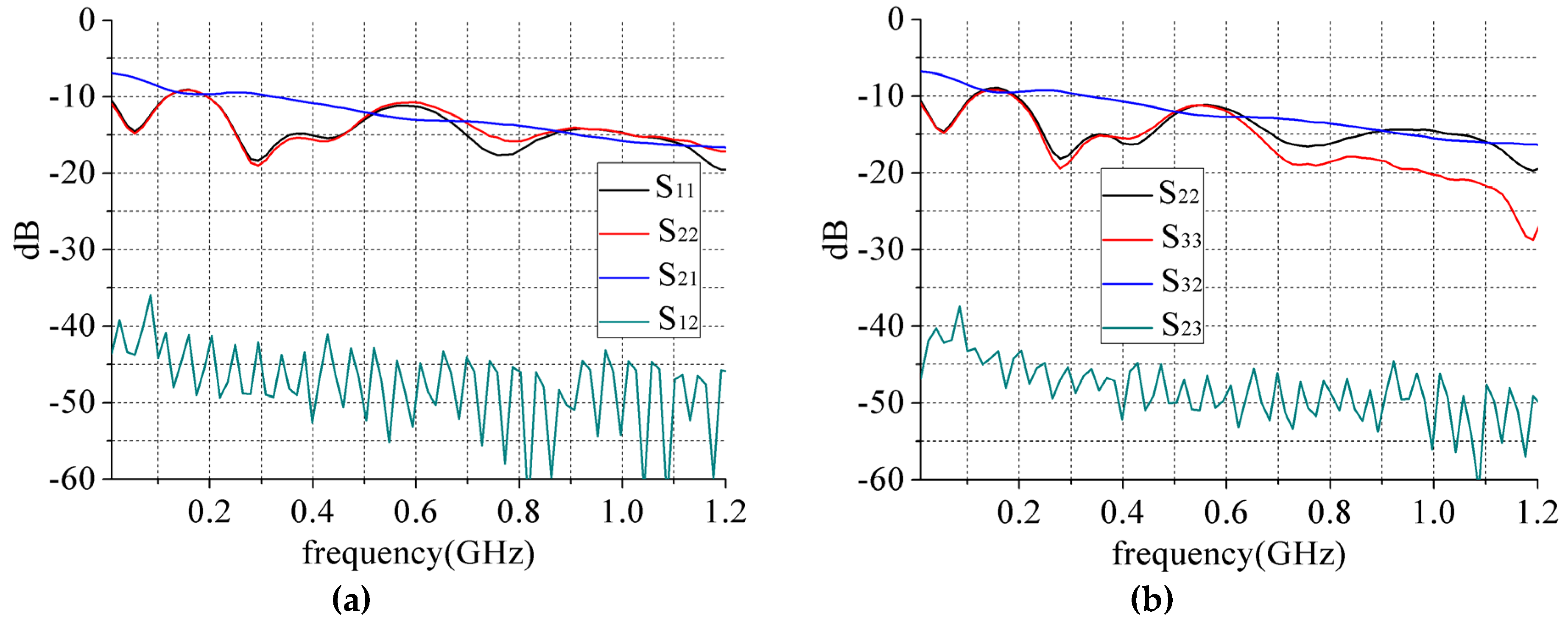
3.1. Circulator
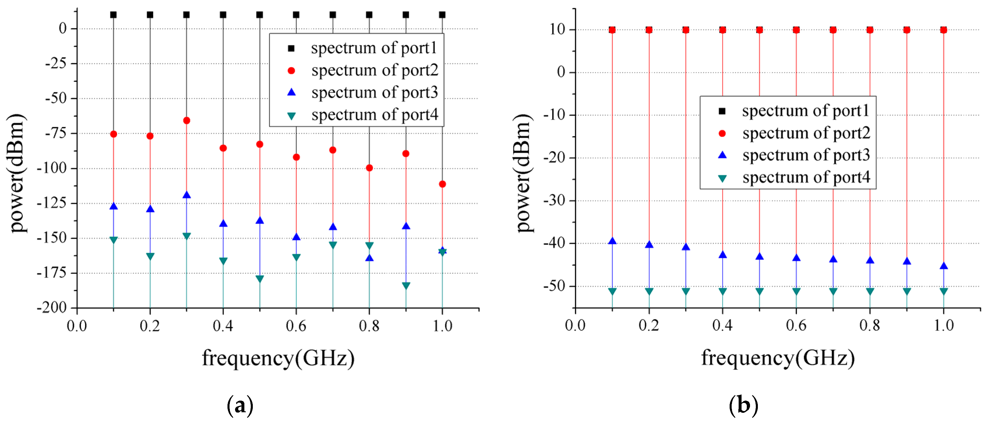
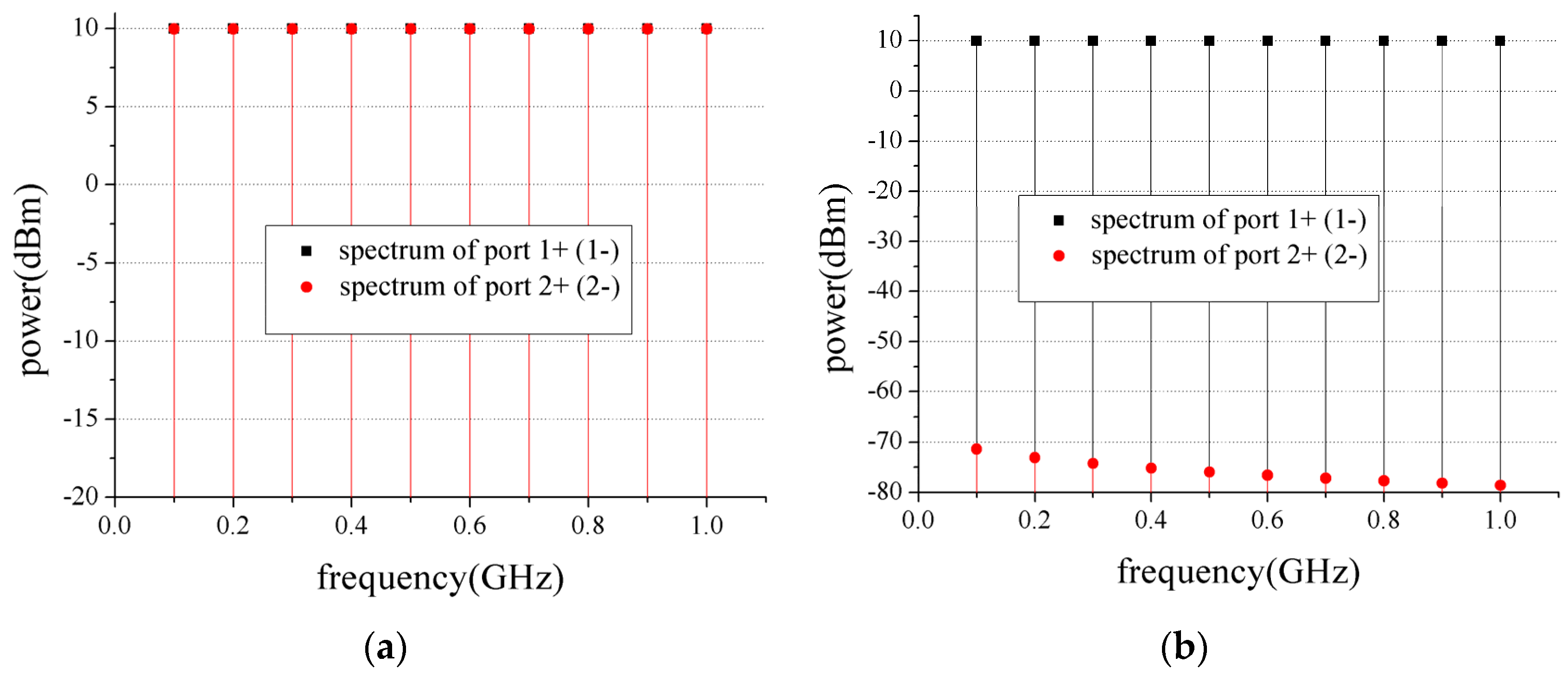
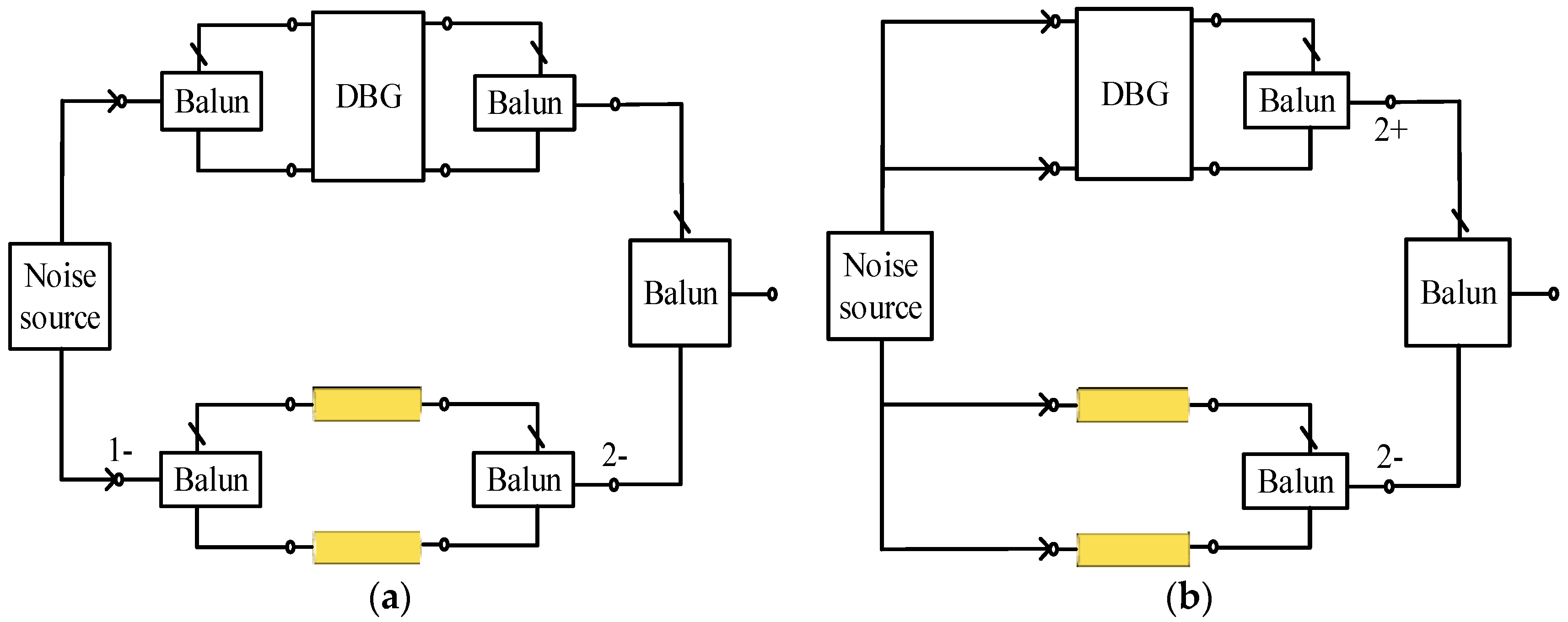
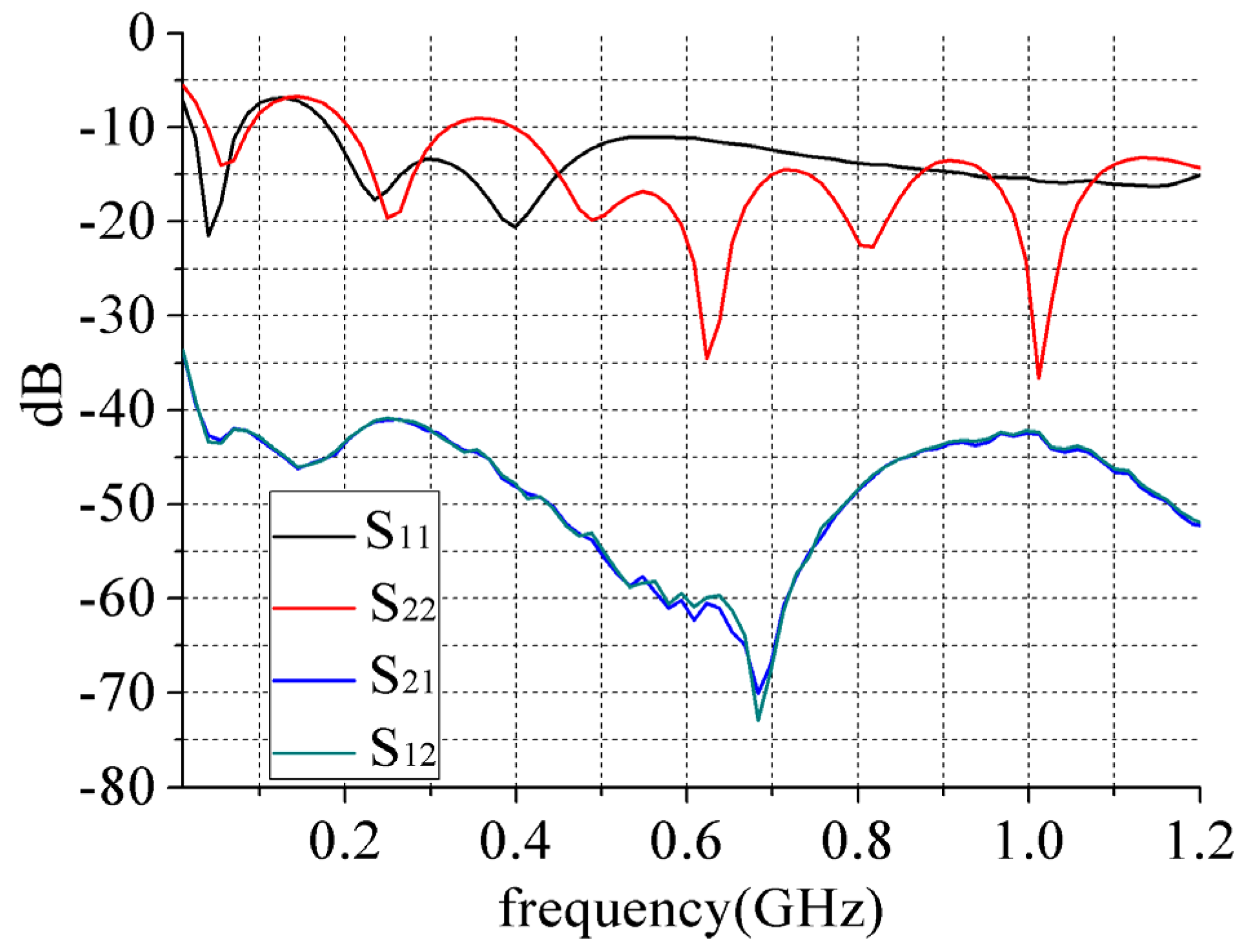
3.2. Isolator
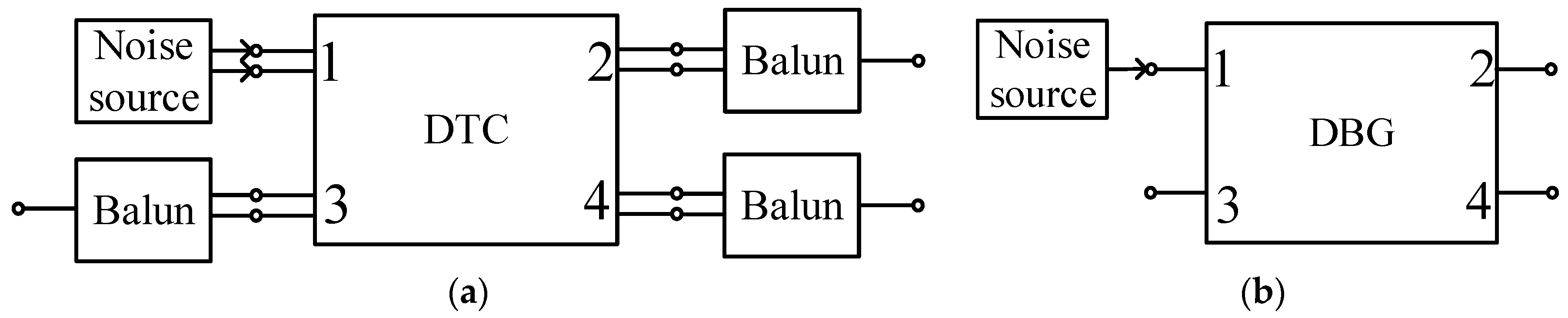
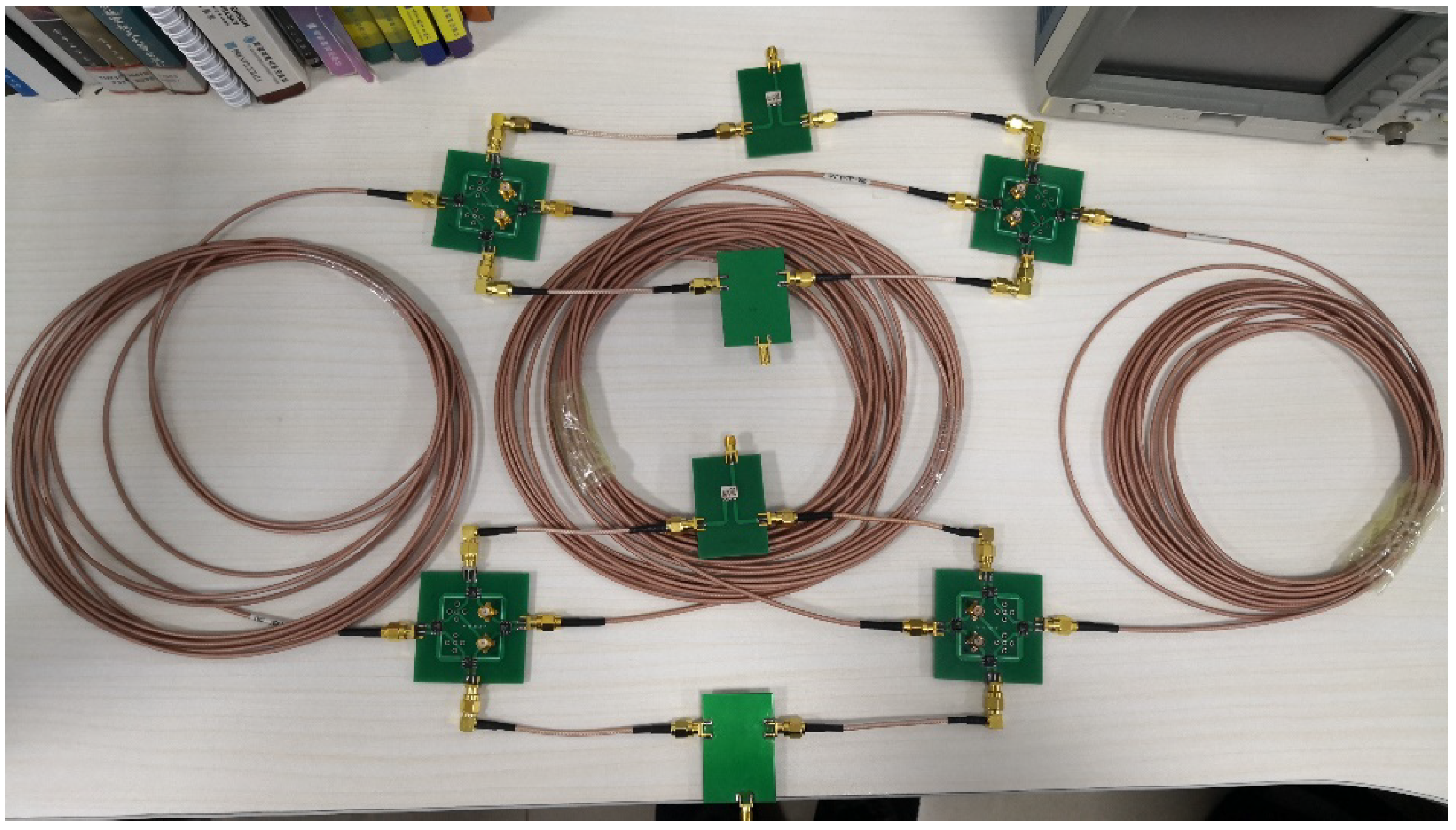
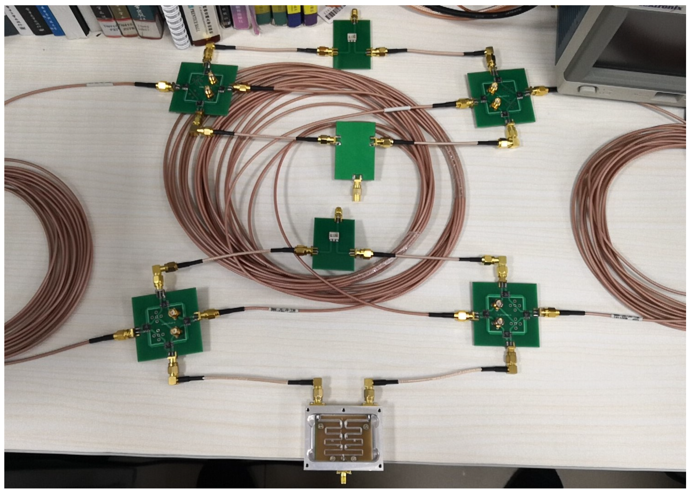
4. The Experiments of the Magnetic-Free Nonreciprocal Device
5. Conclusions
Author Contributions
Funding
Acknowledgments
Conflicts of Interest
References
- Dong, H.; Smith, J.R.; Young, J.L. A Wide-Band, High Isolation UHF Lumped-Element Ferrite Circulator. IEEE Microw. Wirel. Compon. Lett. 2013, 23, 294–296. [Google Scholar] [CrossRef]
- Zeng, L.; Tong, C.E.; Blundell, R.; Grimes, P.K.; Paine, S.N. A Low-Loss Edge-Mode Isolator With Improved Bandwidth for Cryogenic Operation. IEEE Trans. Microw. Theory Tech. 2018, 66, 1–7. [Google Scholar] [CrossRef]
- Liberal, I.; Engheta, N. Erratum: Near-zero refractive index photonics. Nat. Photonics 2017, 11, 264. [Google Scholar] [CrossRef]
- Pacheco-Peña, V.; Beruete, M.; Rodríguez-Ulibarri, P.; Engheta, N. On the performance of an ENZ-based sensor using transmission line theory and effective medium approach. New J. Phys. 2019, 21, 043056. [Google Scholar] [CrossRef] [Green Version]
- Wang, S.; Lee, C.H.; Wu, Y.B. Fully integrated 10-GHz active circulator and quasi-circulator using bridged-T networks in standard CMOS. IEEE Trans. Very Large Scale Integr. Syst. 2016, 24, 3184–3192. [Google Scholar] [CrossRef]
- Mung, S.W.Y.; Chan, W.S. Active Three-Way Circulator Using Transistor Feedback Network. IEEE Microw. Wirel. Compon. Lett. 2017, 27, 476–478. [Google Scholar] [CrossRef]
- Popa, B.I.; Cummer, S.A. Nonreciprocal active metamaterials. Phys. Rev. B 2012, 85, 205101. [Google Scholar] [CrossRef]
- Estep, N.A.; Sounas, D.L.; Alu, A. Magnetless Microwave Circulators Based on Spatiotemporally Modulated Rings of Coupled Resonators. IEEE Trans. Microw. Theory Tech. 2016, 64, 502–518. [Google Scholar] [CrossRef]
- Kord, A.; Sounas, D.L.; Alu, A. Pseudo-Linear Time-Invariant Magnetless Circulators Based on Differential Spatiotemporal Modulation of Resonant Junctions. IEEE Trans. Microw. Theory Tech. 2018, 66, 2731–2745. [Google Scholar] [CrossRef]
- Qin, S.; Xu, Q.; Wang, Y.E. Nonreciprocal Components With Distributedly Modulated Capacitors. IEEE Trans. Microw. Theory Tech. 2014, 62, 2260–2272. [Google Scholar] [CrossRef]
- Reiskarimian, N.; Zhou, J.; Chuang, T.H.; Krishnaswamy, H. Analysis and Design of Two-Port N-Path Band-Pass Filters with Embedded Phase Shifting. Circuits and Systems II: Express Briefs. IEEE Trans. 2016, 63, 728–732. [Google Scholar]
- Reiskarimian, N.; Zhou, J.; Krishnaswamy, H. A CMOS Passive LPTV Nonmagnetic Circulator and Its Application in a Full-Duplex Receiver. IEEE J. Solid State Circuits 2017, 52, 1358–1372. [Google Scholar] [CrossRef]
- Dinc, T.; Nagulu, A.; Krishnaswamy, H. A Millimeter-Wave Non-Magnetic Passive SOI CMOS Circulator Based on Spatio-Temporal Conductivity Modulation. IEEE J. Solid State Circuits 2017, 52, 3276–3292. [Google Scholar] [CrossRef]
- Dinc, T.; Tymchenko, M.; Nagulu, A.; Sounas, D.; Alu, A.; Krishnaswamy, H. Synchronized conductivity modulation to realize broadband lossless magnetic-free non-reciprocity. Nat. Commun. 2017, 8, 795. [Google Scholar] [CrossRef] [PubMed]
- Nagulu, A.; Dinc, T.; Xiao, Z.; Tymchenko, M.; Sounas, D.L.; Alù, A.; Krishnaswamy, H. Nonreciprocal Components Based on Switched Transmission Lines. IEEE Trans. Microw. Theory Tech. 2018, 66, 4706–4725. [Google Scholar]
- Lu, R.; Krol, J.; Gao, L.; Gong, S. A Frequency Independent Framework for Synthesis of Programmable Non-reciprocal Networks. Sci. Rep. 2018, 8, 14655. [Google Scholar] [CrossRef] [PubMed] [Green Version]
- Fengchuan, W.; Yuejun, Z.; Fang, Y.; Yunqi, F. Magnetic-Free Isolators Based on Time-Varying Transmission Lines. Electronics 2019, 8, 684. [Google Scholar] [Green Version]


© 2019 by the authors. Licensee MDPI, Basel, Switzerland. This article is an open access article distributed under the terms and conditions of the Creative Commons Attribution (CC BY) license (http://creativecommons.org/licenses/by/4.0/).
Share and Cite
Wu, F.; Zheng, Y.; Fu, Y. Magnetic-Free Nonreciprocal Multifunction Device Based on Switched Delay Lines. Electronics 2019, 8, 862. https://doi.org/10.3390/electronics8080862
Wu F, Zheng Y, Fu Y. Magnetic-Free Nonreciprocal Multifunction Device Based on Switched Delay Lines. Electronics. 2019; 8(8):862. https://doi.org/10.3390/electronics8080862
Chicago/Turabian StyleWu, Fengchuan, Yuejun Zheng, and Yunqi Fu. 2019. "Magnetic-Free Nonreciprocal Multifunction Device Based on Switched Delay Lines" Electronics 8, no. 8: 862. https://doi.org/10.3390/electronics8080862
APA StyleWu, F., Zheng, Y., & Fu, Y. (2019). Magnetic-Free Nonreciprocal Multifunction Device Based on Switched Delay Lines. Electronics, 8(8), 862. https://doi.org/10.3390/electronics8080862