1. Introduction
The demand of communication technology for integrating more communication standards within one space-restricted equipment is increasing, especially with the rise in Bluetooth, WiFi, WLAN, and WiMAX systems. To enhance the antenna’s performance, different methods have been used, such as insertion of slots/slits and the use of metamaterials. Metamaterials are engineered materials that show controllable electromagnetic characteristics that are not available in natural conventional materials. The unusual characteristics of metamaterials include negative refraction, left-handed characteristics, sub-wavelength focusing, enhanced antenna performance, etc. Victor Vassalago, in 1967 first observed material with simultaneous negative permittivity and permeability at certain frequency, which were not available in the natural conventional material [
1]. Later, John Pendry presented a summary of metallic microstructure comprising a regular array of thin wires that displayed a negative permittivity in 1996 and wire configuration on nonmagnetic thin sheets of metal with a negative permeability in 1999 [
2]. Smith et al. then demonstrated a composite material whose permittivity and permeability were simultaneously negative [
3]. Nowadays, different shapes like, “S-shaped”, “π-shaped” [
4], and “tree-shaped” [
5] metamaterial structures have been designed for various applications, such as electromagnetic cloaking, specific absorption rate (SAR) reduction, antenna application, and filter application [
6]. A dual band “double Z-shape” left-handed metamaterial was presented by Zhou et al. in 2016, where the dimensions of a single unit cell was 8.50 × 8.50 mm
2, resonance at C- and X-bands, and effective medium ratio was 4.80 [
7]. In [
8], Liu et al. presented a modified circular electric resonator which optimize dimension was 5.5 × 5.5 mm
2. The metamaterial showed resonance at the X-band and negative permittivity from 10.20 to 11.70 GHz, as well as negative permeability from 10.20 to 11.40 GHz.
Metamaterial antenna is a category of antenna where metamaterials are embedded with the antenna’s structure. Using the metamaterials in antenna design leads to size reduction, gain and bandwidth enhancement. A metamaterial-based quad band antenna is presented that was applicable for 880 to 980 MHz and 1580 to 2010 MHz frequency band applications [
9]. A reconfigurable slot antenna was composed by using soldered pin diodes between the sickle-shaped slots in the ground plane for Bluetooth and WiMAX systems. The dimension of the designed antenna was 80 × 80 mm
2, printed on FR-4 dielectric material. The antenna covered a bandwidth of 100 and 190 MHz for Bluetooth, WiMAX applications with the gain of 2.33, 3.59 dBi at 2.46 and 3.59 GHz, respectively [
10]. In [
11], Martínez et al. presented a dual-band monopole antenna that covered the Bluetooth band, and the antenna’s size was 40 × 30 mm
2. Miniaturized planer antennas are studied based on resonators. Dong et al. proposed a dual band antenna, where the gain and bandwidth at 2.40 GHz were 2.02 dBi and 100 MHz, and the antenna’s size was 34 × 34 mm
2 [
12]. A compact quad-band antenna based on open loop resonators (OLRs) is presented where the antenna’s size was 40 × 35 mm
2, fabricated on FR-4 substrate. The metamaterial antenna showed resonance points at 2.45 GHz, 3.52 GHz, 4.65 GHz, and 6.05 GHz, which are compatible for WLAN and RFIDs applications [
13]. Two metamaterial antennas applied for WLAN and WiMAX were suggested by Li et al. Antenna-1 was composed of a monopole radiator with an ELC element for the frequency band of 2.49 to 2.55 GHz and 3.0 to 3.68 GHz. In addition, antenna 2 was integrated with the EBG structure to achieve bands of 2.49 to 2.53 GHz and 2.95 to 4.0 GHz. Moreover, both antennas covered the WiMAX in a 2.5/3.5-GHz operational band with omnidirectional radiation patterns [
14]. Bala et al. presented a modified electrically ELC structure-based antenna, with a bandwidth of 530 MHz (2.40 to 2.93 GHz) and gain of 1.5 dBi for WiMAX applications. The overall antenna size was 40 × 45 mm
2 [
15]. Two tri-band metamaterial antennas loaded with triangular electromagnetic resonator (TER), and complementary TER (CTER) were suggested by Zhu et al. Where, antenna-1 was operated in the frequency bands of sequentially 1.78–1.84, 3.34–3.86, and 5.75–5.87 GHz, which covered the bands for WLAN and WiMAX applications. Antenna-2 improved the impendence matching of 5.75–5.87 GHz, without influencing the first two bands of antenna-1. The overall size of the antenna was 38 × 35 mm
2 with a bandwidth of 100 MHz (band 1), 520 MHz (band 2), and 120 MHz (band 3) [
16]. A penta-band CPW-fed monopole antenna was designed using metamaterial on FR4 dielectric material for GSM-1800, UMTS and lower WLAN frequency bands [
17]. A single-layer rectangular patch with ‘Q’ slot antenna was designed for frequency bands of 2.4–2.56 GHz (WiFi) and 3.43–3.78 GHz (WiMAX) applications [
18]. A compact MIMO antenna (Nandi et al. 2017), was designed on Rogers RT 5880 and applicable for WLAN (2.37–2.64 GHz) and WiMAX (3.39–3.58 GHz) [
19]. A wideband quad-polarization reconfigurable meta-surface antenna consisting of a square patch, a meta-surface layer, and four feeding probes with a switchable feeding network. By properly selecting the feeding probes, the proposed antenna could work at four polarization states, namely X-linear polarization (X-LP), Y-linear polarization (Y-LP), left-hand circular polarization (LHCP), and right-hand circular polarization (RHCP). The antenna’s size was 70 × 70 mm
2 on a RO4350 substrate [
20]. A triple-band antenna was presented for frequency bands of 1.55 to 1.67 GHz, 2.2 to 3 GHz, and 5.13 to 6 GHz for GPS, LTE, WLAN, Wi-Fi, and WiMAX systems, respectively [
21]. A microstrip-grid antenna had the dimensions of 297 × 210 mm
2 operates from 2.38 to 2.51 GHz for WiFi applications [
22].
In this paper, we present a single layer metamaterial inspired antenna, where the square-circular SRR metamaterial was incorporated with the patch of the antenna. The antenna was excited with a microstrip zig-zag shaped feed line printed on the FR-4 dielectric material. The integrated metamaterial structure exhibited double negative characteristics and was compact in size. The proposed metamaterial antenna is applicable for Bluetooth, WiFi, WLAN, and WiMAX.
2. Design of the Metamaterial Antenna
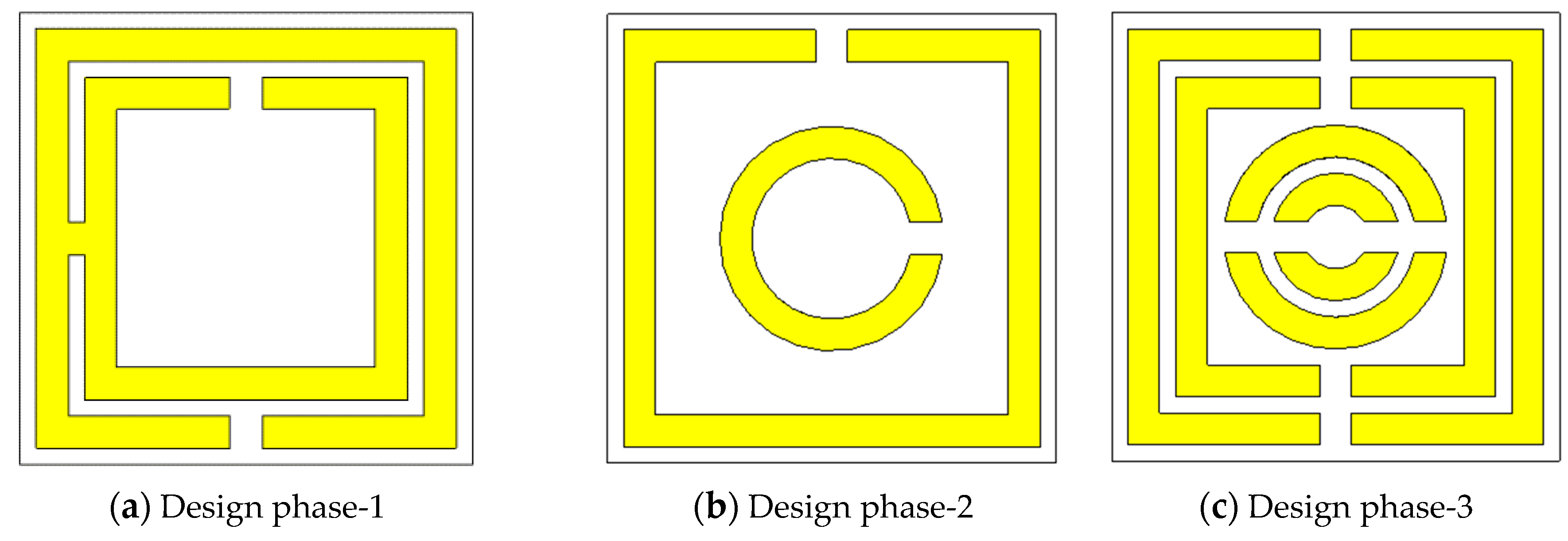
Metamaterials are usually implemented by periodic unit cells, in which the thickness, size of the total cells, metallic strips and splits are essential parameters. Wide operational bandwidth is obtained using multi resonance, multilayer, and passive elements, while the cell size usually is related to the design techniques and current density distribution. Although current path can be increased by bending the shapes for compactness but this approach increases unwanted coupling effects and decreases operational bandwidth. The designed metamaterial structure behaves like inductive-capacitive lumped circuit, where resonances are generating into the structure by metal strips and split gaps. The metal strip is excited through a time changing magnetic field and electrostatic field is induced in the split gape and inductive current in the metal strip. The inductive and capacitive effects are produced by adopting a printed metallic stripe and gap between the stripes. The length of the metal arms is responsible for creating an inductive effect and the spilt between the stripes. The circular ring resonators are responsible for the capacitive effect. The presented metamaterial is analyzed for designing a compact metamaterial structure (
Figure 1a–d).
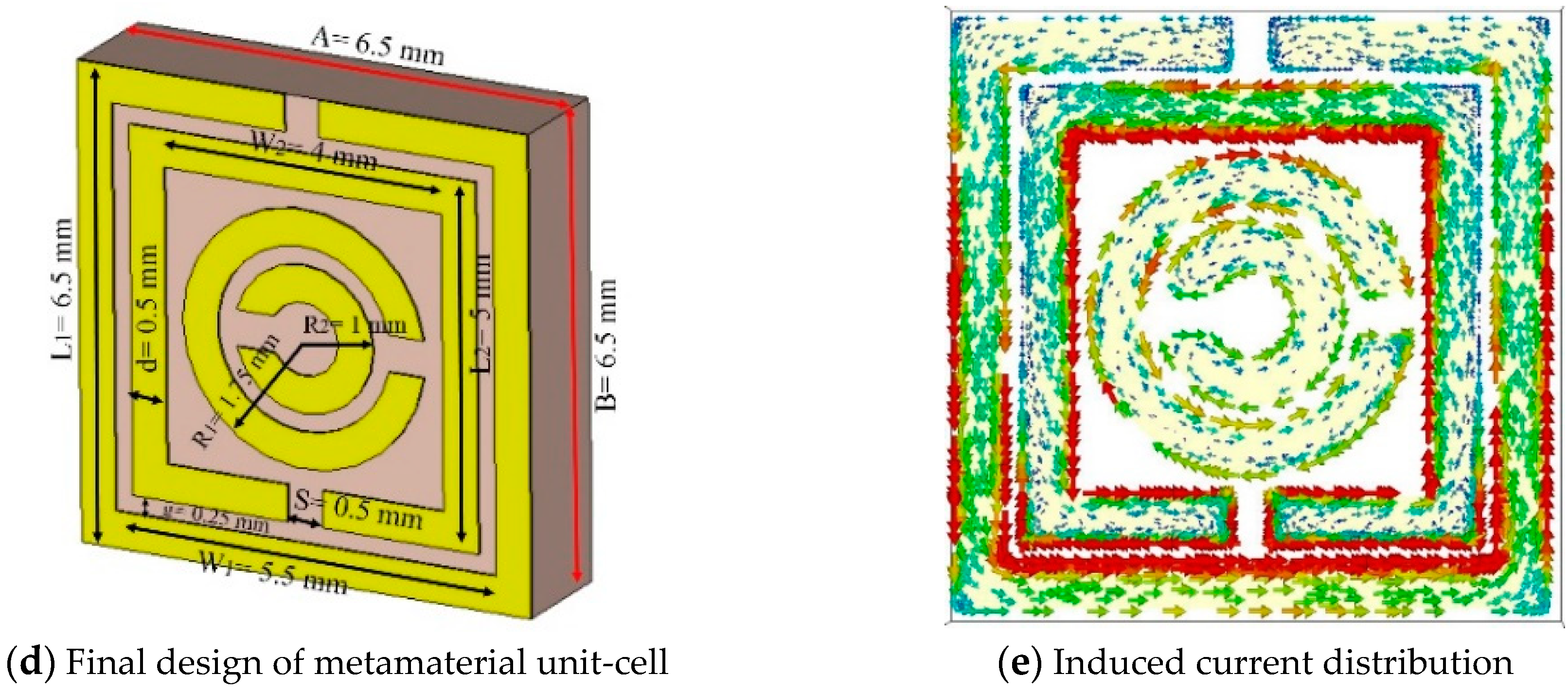
In
Figure 1d, the outer square metallic ring resonator has a length, width and split of 6.5, 5.5, and 0.50 mm, respectively. In addition, the inner square ring resonator has a width and length of 5.0 and 4.0 mm, as well as a split of 0.50 mm. Inside the inner ring resonator there are two circular ring resonators with the split etched on both circular ring resonators. The radius of the first and second circular ring resonators were respectively, 1.75 and 1.0 mm, whereas 0.50 mm splits were etched on the circular ring resonator. The width of every square and circular ring resonator was 0.50 mm, and the gap between every ring resonator was 0.25 mm. In addition, the length (A) and width (B) of the FR-4 substrate material were both 6.5 mm each, with a thickness of 1.60 mm. However, the overall dimension of the embedded metamaterial unit cell was 6.50 × 6.50 mm
2.
Figure 1e shows the induced current distribution of the designed metamaterial unit-cell. The square and circular resonators were made to radiate, while the splits and the gap between the resonators matched the impedance. There is strong induced current distribution on the inner side of the resonators. The inner square-shape resonator has more radiation and the current is follow in the same direction. The circular resonators have less effect on the radiation and reduce the mutual coupling which helps for the impedance match.
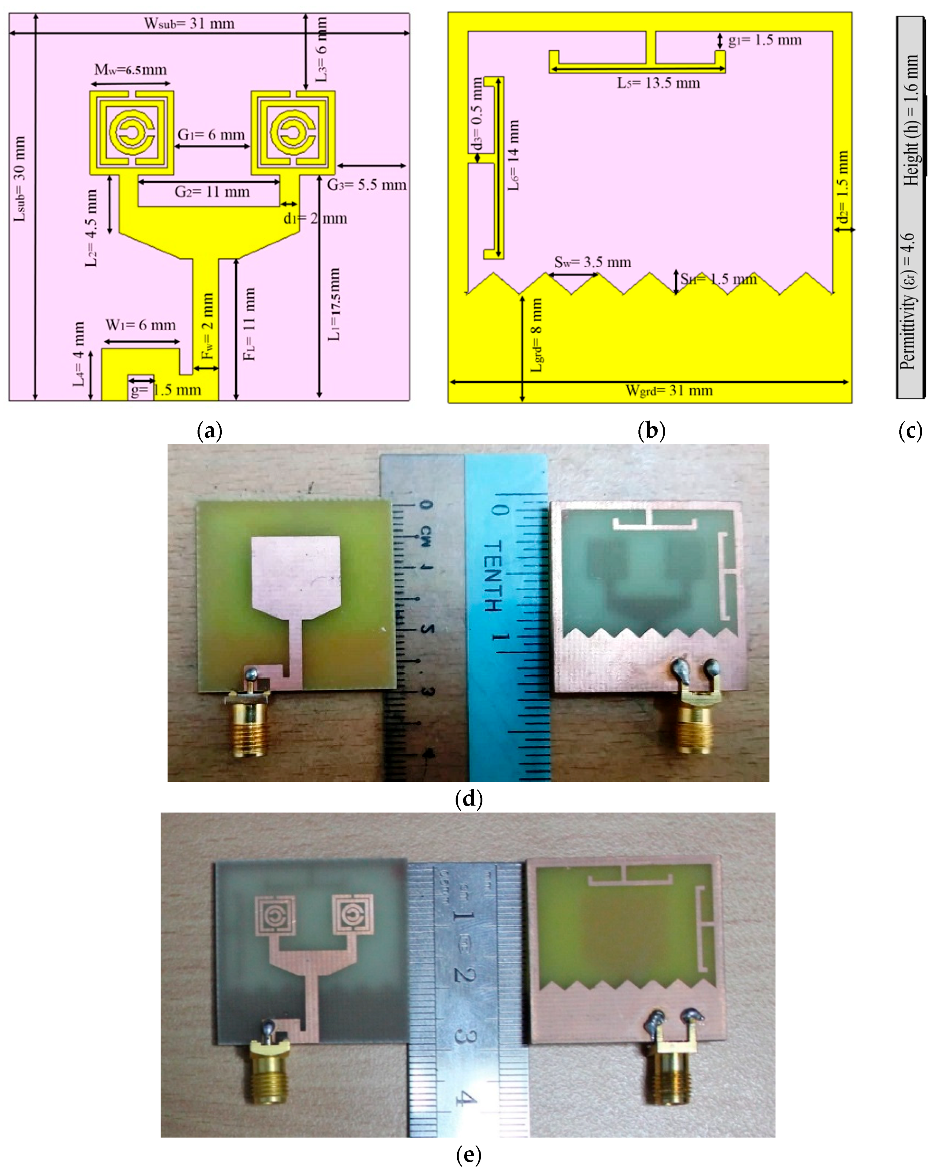
The antenna geometry is fabricated on a single layer Epoxy resin fibre dielectric material (permittivity of 4.60, loss tangent of 0.02 and thickness of 1.60 mm). FR-4 is a composite dispersive material composed of woven fiberglass cloth with an epoxy resin binder that is flame resistant. FR-4 glass epoxy is a popular and versatile high-pressure thermoset plastic laminate grade. The final geometry of the antenna with and without metamaterial is depicted in
Figure 2a–e. The antenna was excited through a microstrip zig-zag shaped feed line which was printed on the bottom layer of substrate and a 50 Ω SMA connector was connected the feed line and ground plane. In
Figure 2a, two metamaterial unit cells are placed parallel with a 6.0 mm separation and located 6.0 mm away from the antenna top edge. A zig-zag feed line, length of 4.0 mm was placed at the bottom edge of antenna and total length of feed line was 11 mm, whereas the width was 2.0 mm.
Figure 2b,c is shown the back view and the cross-sectional view of the proposed metamaterial embedded antenna. In the back side, defected ground technique was used to improve the antenna’s bandwidth. Triangular shaped slots (height of S
H = 1.5 mm and width of S
W = 3.5 mm) were made on the top edge of ground plane and two additional “T-shaped” metallic strips length of L
5 = 13.5 mm and L
6 =14 mm relates to the square metallic arm joint with the slotted ground plane. Moreover, the slotted ground plane and additional “T-shaped” metallic strips were used to improve the antenna bandwidth. The slots were induced electromagnetic coupling and tuneable capacitance.
Figure 2d,e shows the without metamaterial and with metamaterial antenna. The dimension of the proposed metamaterial inspired antenna is 30 × 31 mm
2 (L × W) and antenna design specifications are given in
Table 1.
3. Methodology and Measurement System
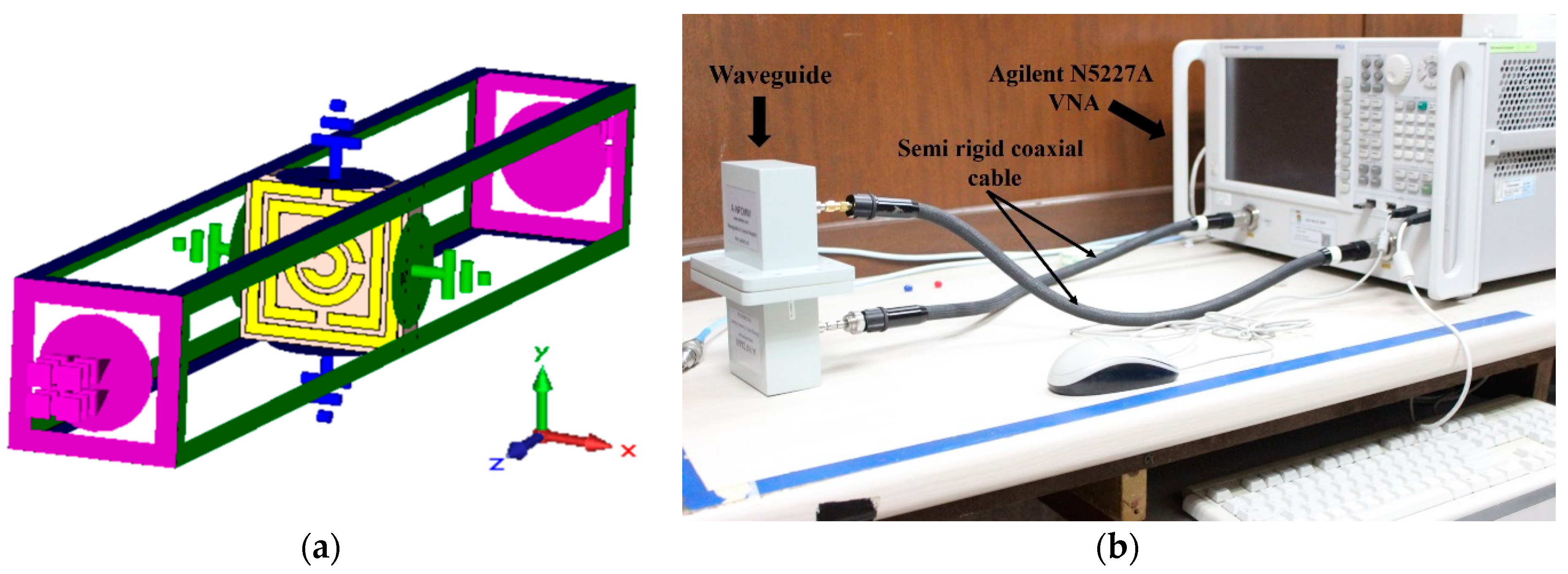
Electromagnetic simulation helps evaluating the fundamental field quantities from Maxwell’s equation by adopting the numerical method. Proper selection of feeding technique, meshing of structure, appropriate boundary conditions are important for analysis and optimize design. In this research, CST Microwave Studio electromagnetic simulator was adopted for numerical investigations and boundary conditions were used to speed up the computation process in case of metamaterial structure [
23]. Perfect electromagnetic conductor (PEMC) boundary condition was the generalization of perfect electric conductor and perfect magnetic conductor used for simulations. This PEMC boundary condition has the advantages of decreased cross section sizes and speeding calculation times. Perfect electric and magnetic conductor were applied along the walls of
x-axis and
y-axis, respectively, as well as electromagnetic waves are incident along z-axis in metamaterial simulation, which is shown in
Figure 3a. For the measurement of designed metamaterial two rectangular 510WCAS, 340WCAS, and 187WCAS waveguide to coaxial adapters are utilized. The waveguides are connected to the Agilent N5227A vector network analyser by the semi rigid coaxial cable and connectors. The fabricated prototype is placed between the transmitter and receiver wave-guide to measure the reflection and transmission coefficients shown in
Figure 3b.
Nicolson–Ross–Weir (NRW) method [
24,
25] is adopted for the characterization of designed metamaterial strucutre. The numerical calculation process of the effective parameters are as follows:
where ‘
d’ is the thickness of substrate, ‘
S11’ is the reflection coefficient and ‘
S21’ is the transmission coefficient, ‘
c’ is the velocity of light and ‘
f’ is the resonance frequency. The reactance impedance is directly extracted from the complex reflection and transmission coefficients that can be expressed as,
where ‘
’ is the relative impedance, ‘
T’ is the transmission coefficient and ‘
R’ is the reflection coefficient. The ring resonators produce a magnetic susceptibility (
) associated with area and inductance loaded with capacitance [
26].
where normal incidence
and angular frequency
. The ring resonator produce a magnetic two-time derivative Lorentz material described by its magnetization field behaviours in the time and frequency domains as,
where ‘
’ is the magnetic susceptibility, ‘
’ is the magnetization (magnetic moment per unit volume), ‘
’ is the applied magnetizing field intensity and ‘
’, ‘
’, ‘
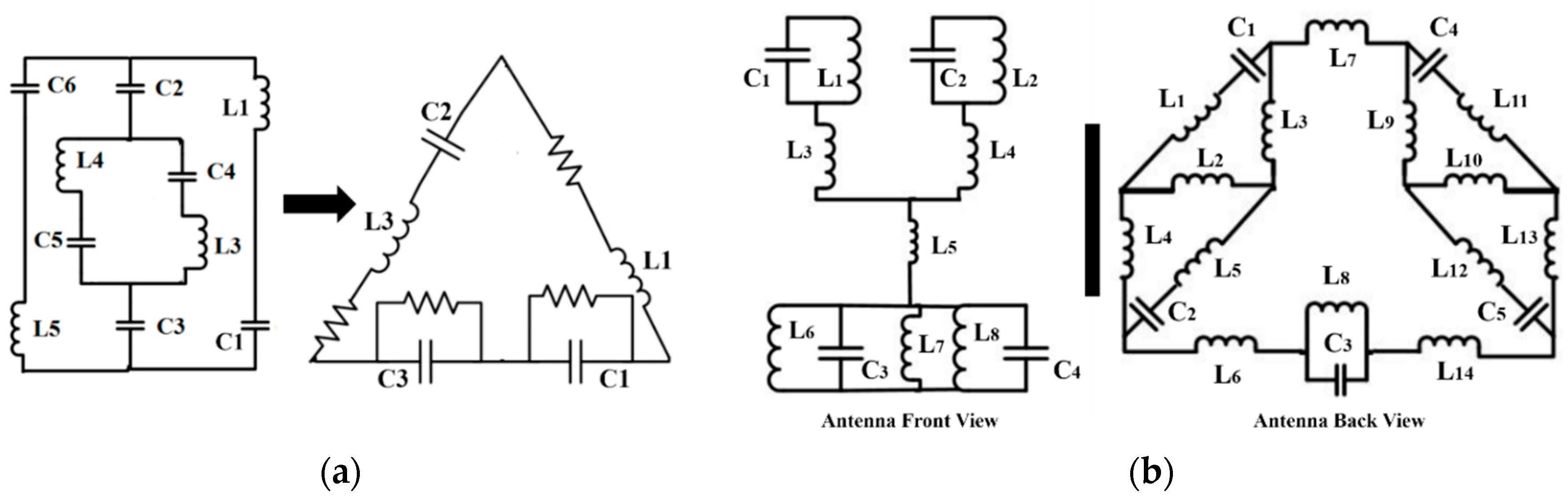
’ are the material constants. The equivalent lumped-element circuit of the metamaterial unit cell and antenna structures are given in
Figure 4a,b, where the metal sections are formed inductance and the splits are responsible for capacitance. By increasing the metal sections in the design structure, the inductive effect is increased, and the resonances are shifted towards the lower frequency. Similarly, by increasing the number of splits and the gaps between the resonators, the capacitive effects can be raised and the resonances will be shifted towards the higher frequency [
27]. In the circuit diagram, the splits and gaps are symbolized by C
1, C
2, C
3, C
4, C
5, and C
6. Conversely, the metal sections are denoted by L
1, L
2, L
3, L
4, L
5, L
6, L
7, L
8, L
9, L
10, L
11, L
12, L
13, and L
14.
According to the strip line theory [
28], the inductance of the strips line is calculated using,
where ‘
l’ is the length of the strip line, ‘
w’ is the width and ‘
t’ is the thickness. The capacitance per unit length of the paralleled strip lines are calculated using [
29,
30],
where ‘
’ is the permittivity of the free space,
and
F(
k) are calculated as,
where
.
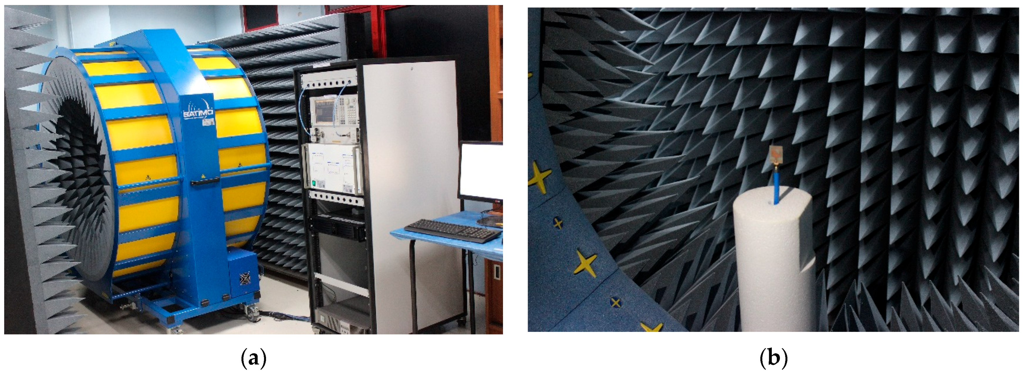
After successful design and analysis, the prototype of the proposed metamaterial antenna was measured for experimental verification. Vector network analyzer (VNA) is a typical instruments for metamaterial-based antenna measurement. The Agilent technologies N5227A PNA microwave network analyzer was used for measurement, which was calibrated by the Agilent N4694-60001 ECal for error free measurement. Scattering parameters, VSWR were measured by connecting the metamaterial structure through the waveguide method and metamaterial antenna individually to the network analyzer via a semi-rigid cable. The radiation characteristics of the metamaterial inspired antenna has been measured in an anechoic chamber based Satimo Star Lab (650 MHz to 18.0 GHz). The fabricated metamaterial inspired antenna is placed on the test board, which is located at the center of a circular “arch” that contains 16 probes, and the spacing between two probes is 22.5°. The antenna was rotated horizontally through 360° and array of 16 probes give a full wave 3D-scan of the under tested antenna [
28]. Inside the anechoic chamber, the absorbers were used to absorb the unwanted reflected signal and increase the efficiency of metamaterial antenna shown in
Figure 5a,b.
4. Results and Discussions
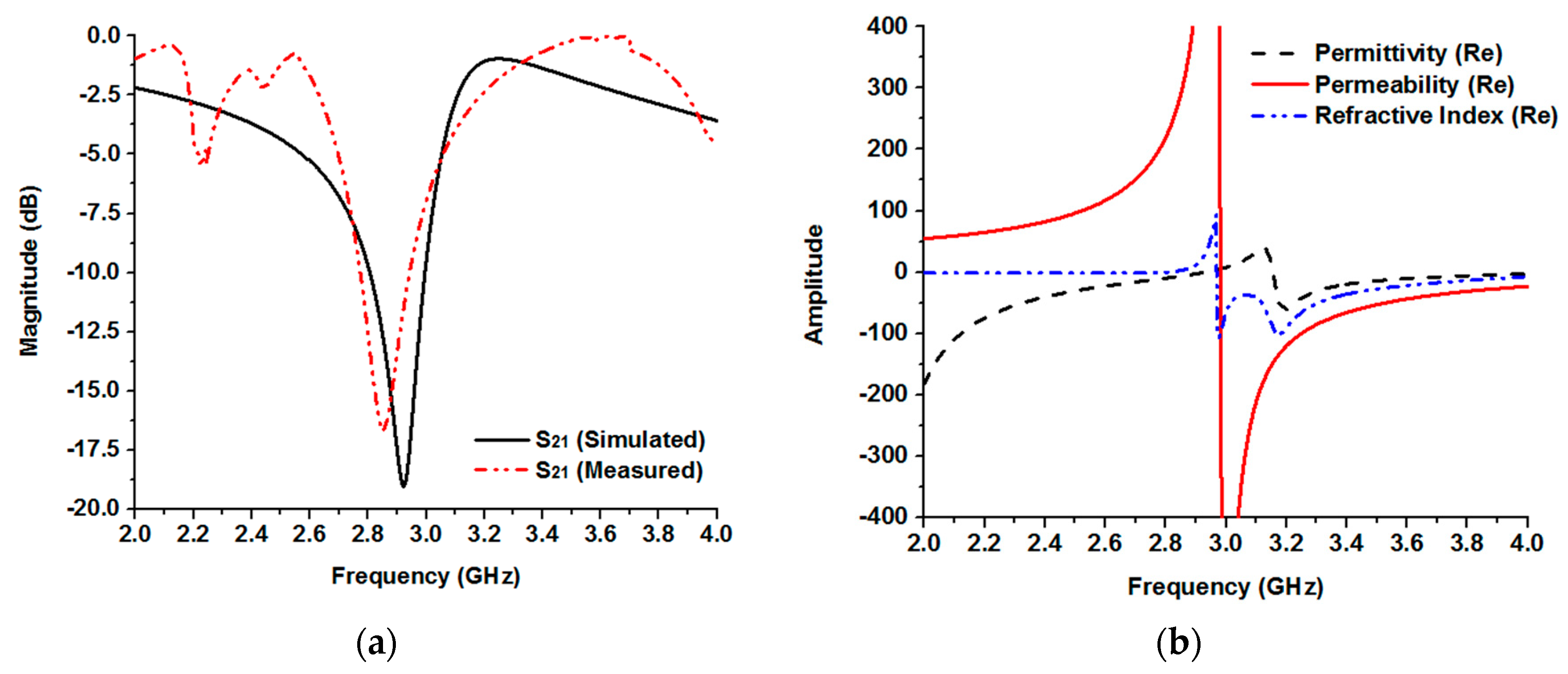
To investigate the metamaterial unit cell performances, scattering parameters and effective parameters are shown in
Figure 6a,b. The simulated transmittance (
S21) was at 2.91 GHz whereas the measured transmittance was at 2.86 GHz, which are in
Figure 6a.
Figure 6b and
Table 2 show the real amplitudes of effective permittivity, permeability and refractive index of the designed metamaterial unit cell. From the figure, permittivity has two negative regions of frequency. The first one was from 2.0 to 2.72 GHz and the second one was from 3.16 to 3.81 GHz. On the contrary, permeability shows only one negative band of frequency from 2.98 to 4.0 GHz, whereas the negative refractive was from 2.97 to 3.92 GHz. The left handed characteristic was one of the unusual effective electromagnetic responses of the metamaterial. A metamaterial is called double negative metamaterial, if the effective permittivity and permeability are simultaneously negative and, on that time, refractive index is also negative. The proposed design has the effective negative permittivity, permeability and refractive index from 3.16 to 3.81 GHz. Therefore, the designed metamaterial is called as a left handed or double negative metamaterial. Moreover, the effective medium parameters can be modified or enhanced because the electric fields are strongly concentrated in the splits and gaps between the resonators in the unit cell structure. The gap width plays a significant role in enhancing permittivity. A large amount of surface charge is accumulated on the edge of resonators and results in significantly large dipole moment. High dipole moments in the unit cell resulting from huge charge accumulation, cause large permittivity. To realize high refractive index, permeability also needs to be enhance by suppressing the diamagnetic response.
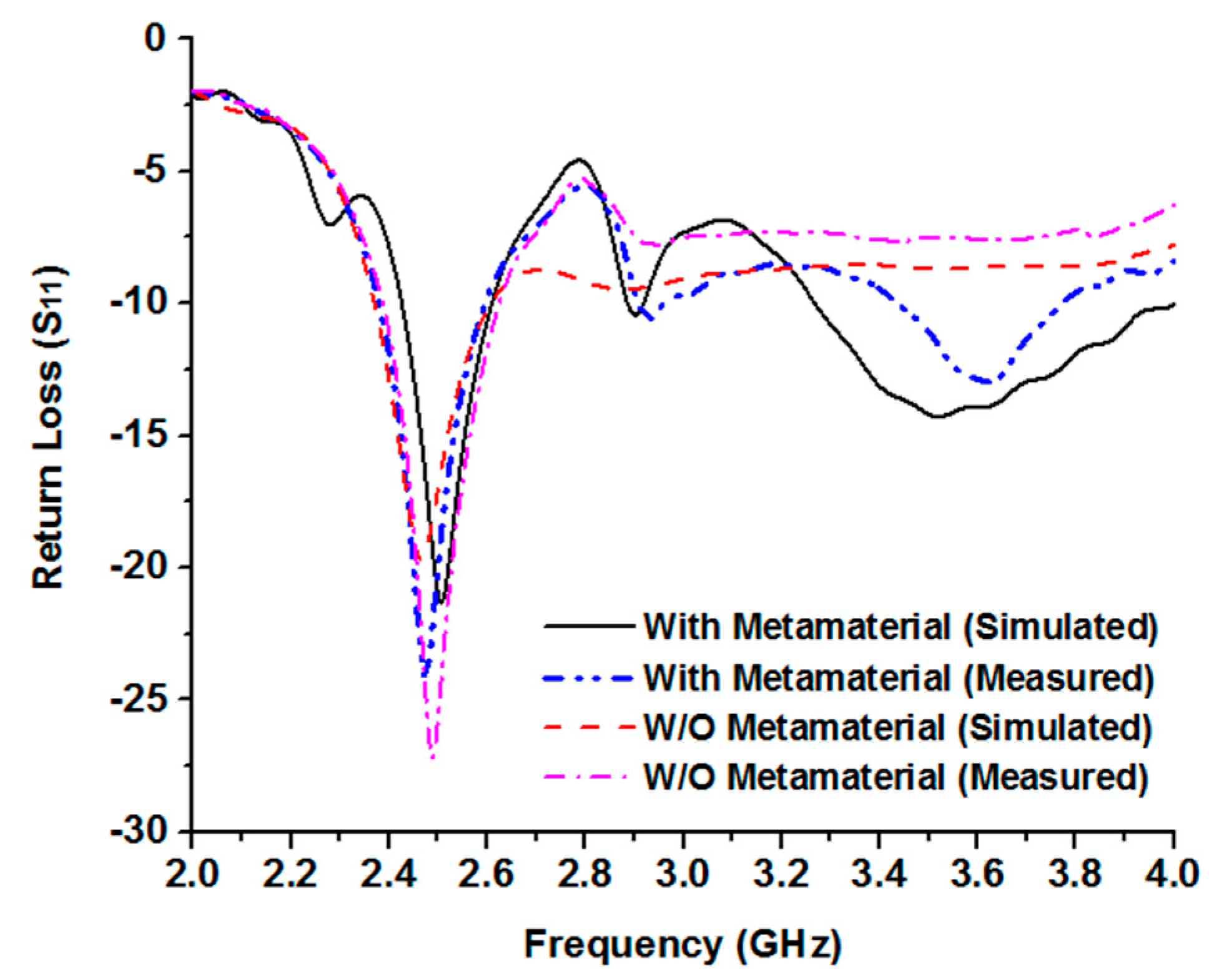
Figure 7 shows the simulated and measured return losses of the proposed metamaterial inspired antenna and without metamaterial antenna. The result displays that the metamaterial loading antenna has two operating frequency band, whereas the conventional antenna has only one band of frequency. The simulated impedance bandwidth of the without metamaterial inspired antenna was from 2.37 to 2.62 GHz and the measured results was from 2.38 to 2.63 GHz. Bandwidth of an antenna can be improved by integrated metamaterial with the antenna. As a result, the metamaterial inspired antenna showed the simulated impedance bandwidth from 2.42 to 2.61 GHz, which covers the Bluetooth, WiFi, WLAN bands and from 3.26 to 3.99 GHz that cover the WiMAX band of frequency. Furthermore, the measured bandwidth was similar to the simulation result from 2.38 to 2.60 GHz and 3.40 to 3.79 GHz, covering the bandwidth of 220 MHz and 390 MHz for Bluetooth (2.40 to 2.485 GHz) bandwidth of 85 MHz; WiFi (2.4 GHz); WLAN (2.40 to 2.49 GHz & 3.65 to 3.69 GHz) bandwidth of 90 MHz and 40 MHz; and WiMAX (3.40 to 3.79 GHz) bandwidth of 390 MHz applications.
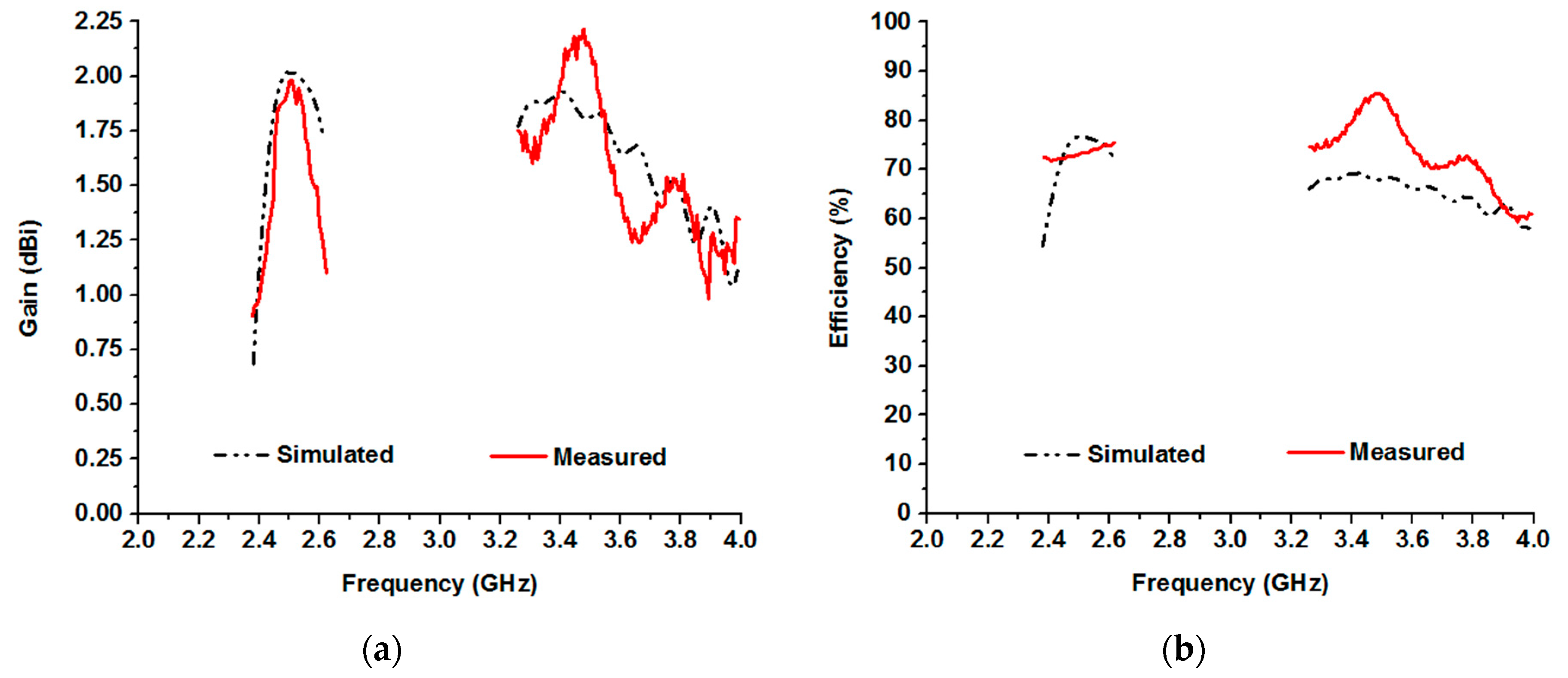
Figure 8a shows the measured and simulated gain of the metamaterial-embedded antenna. In general, antenna gain is related to size, substrate material properties, and multiple layers of the substrate. The proposed metamaterial inspired antenna was compact in size and fabricated on a cost effective single layer FR-4 dielectric material. The metamaterial antenna had a measured average gain of 1.50 dBi, with the minimum and maximum gains of 0.88 and 2.25 dBi, respectively. In addition, antenna gain at 2.47 and 3.62 GHz resonance points were sequentially 1.88 and 1.35 dBi. Moreover, the radiation efficiencies of the metamaterial loading antenna are also shown in
Figure 8b. In the figure the simulated average efficiency 65% and maximum efficiency was 76%, whereas the measured average efficiency was 73%, and maximum efficiency was 85%. However, from
Figure 8a,b it is seen that there is a little discrepancy between the measured and simulated results of the antenna gain and efficiency. There are several reasons behind that, firstly, the permeability of the substrate material is considered as constant in case of simulation but in the fabricated substrate it might be a little bit changed. Secondly, there might be reflection into the field between the antenna under test and probe. The reflection might come from the chamber scattering, antenna holder itself, and the track inside the anechoic chamber. Thirdly, fabrication error of the patch and metamaterial on the dielectric substrate material. Finally, soldering errors of the patch antenna with the SMA connector also one of the reasons for the variation of the simulated and measured results.
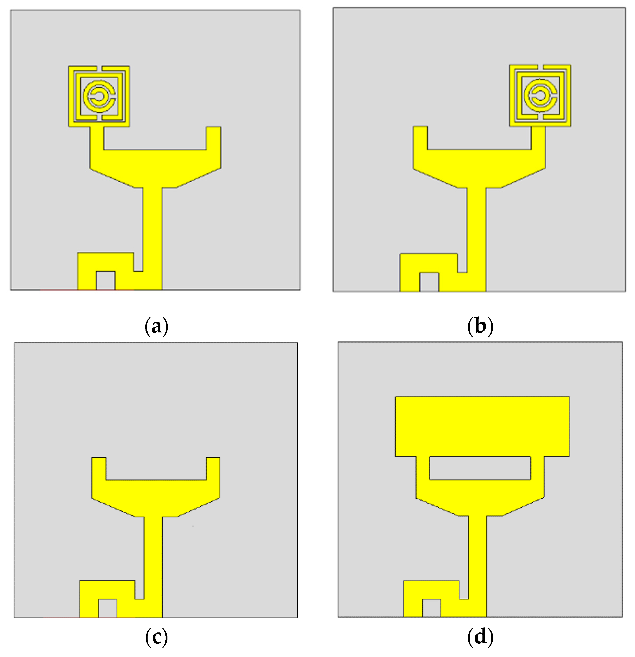
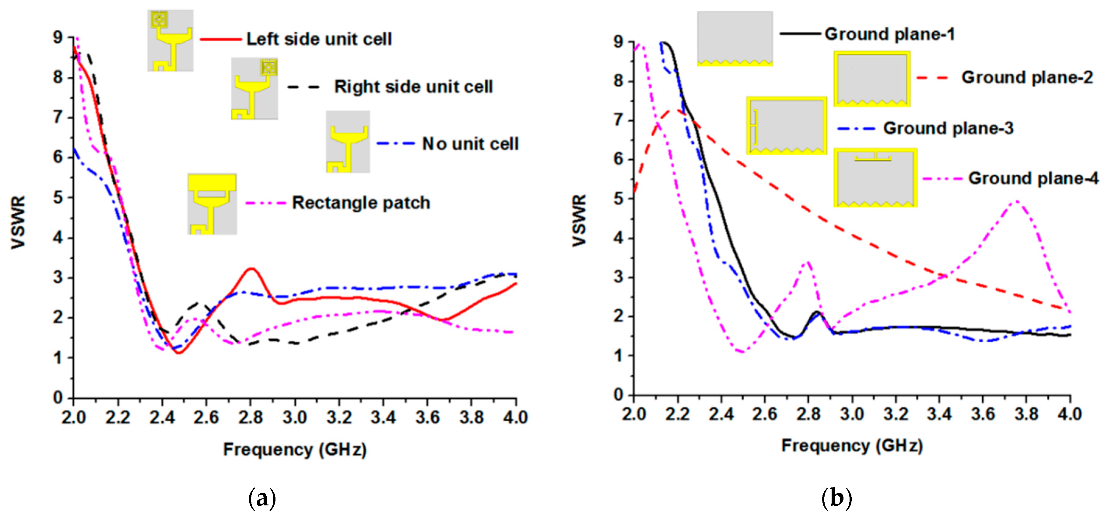
Figure 9a–d show the parametric studies of proposed metamaterial antenna radiating patch structure. In
Figure 9a,b only one metamaterial unit cell is attached sequentially at
Figure 9a left side and
Figure 9b right side. When the ring resonators are added in the radiating patch then the currents are distributing well around the resonators and improve the bandwidth, gain as well as reduce the current on ground plane. Besides, ground plane has some effects on the antenna performance. To minimize the ground effects on antenna performances these ring resonators are added on the antenna patch. In
Figure 9c, there is no any ring resonator, whereas a rectangle patch structure is added replace the ring resonators in
Figure 9d.
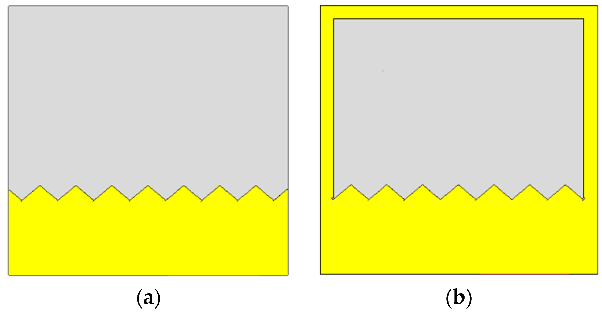
The ground plane has an important impact on resonance frequencies and radiation characteristics. Sometimes, at low frequency operation, an antenna radiating patch is not a good conductor, as a result, conductivity is improved by the ground, additional metal strips, slots, etc. In some cases, ground plane is used as a reflector, in others, as a conductive line, or a part of a waveguide. In
Figure 10a–d, the evaluation of the proposed metamaterial inspired antenna ground plane is displayed and the effects of ground planes on the voltage standing wave ratio (VSWR) are displyed in
Figure 10. In the ground plane, triangular slots and additional T-shaped metallic strips are connected to improve the antenna bandwidth. By making slots in the ground plane, the concentration of the current on the ground increases and it has a major contribution to the antenna’s radiation performance. In addition, high cross-polarization is achieved because of current distribution around the slots on the ground plane. However, dimension of ground plane has effects on antenna impedance match.
The effects of antenna’s different patch structures are shown in
Figure 11a. If the VSWR is lower than 2.0, the antenna impedance match is considered perfect and the antenna performed well, but when VSWR increased above 2, the antenna started to reflect more power and therefore were not transmitted.
Table 3 represents the band of frequencies, where VSWR was lower than 2.0 at different structural arrangements of the proposed antenna configuration.
Figure 11b and
Table 3 illustrate the results of VSWR on different ground planes.
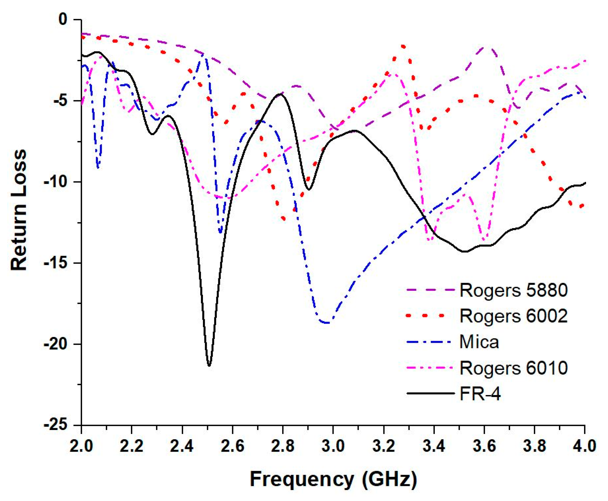
Figure 12 represents the effect on the resonance frequency through various types of materials by using as a substrate material. The dielectric constant of the Rogers RT 5880, Rogers RT 6002, Mica, Rogers RT 6010, and FR-4 were respectively 2.20, 2.94, 5.70, 10.20, and 4.60. If the dielectric constant is increased, then substrate material conductivity is decreased. The permittivity of a material depends on the material’s internal structure. When the EM-waves propagate through a material, then the electric and magnetic fields oscillate as sinusoidal patterns and the velocity of the atoms depend upon the conductivity, whither the conductivity depends on the internal structure. In addition, the internal pattern, permittivity, polarization, etc. caused the variation in the return loss of the antenna.
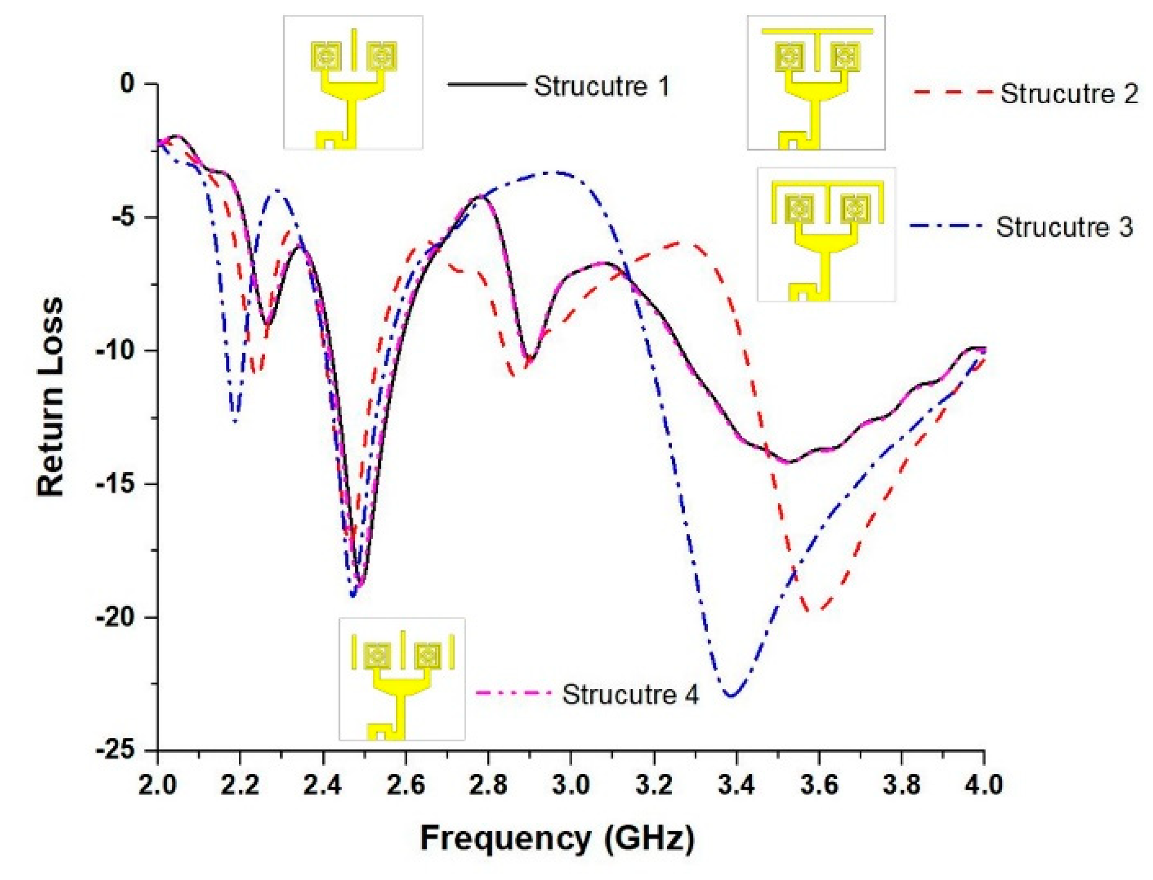
To analysis the isolation mechanism characteristics, antenna horizontal parasitic decoupling strip was designed and placed in the middle and side of the antenna radiating patch. The horizontal strips effectively introduce the desired inductive and capacitive loading of the antenna. The decoupling structures and resuls are shown in
Figure 13. The strips are attached at the top side together and act as transmission line resonators, and effectively reduce the mutual coupling of the radiaiitng resonators.
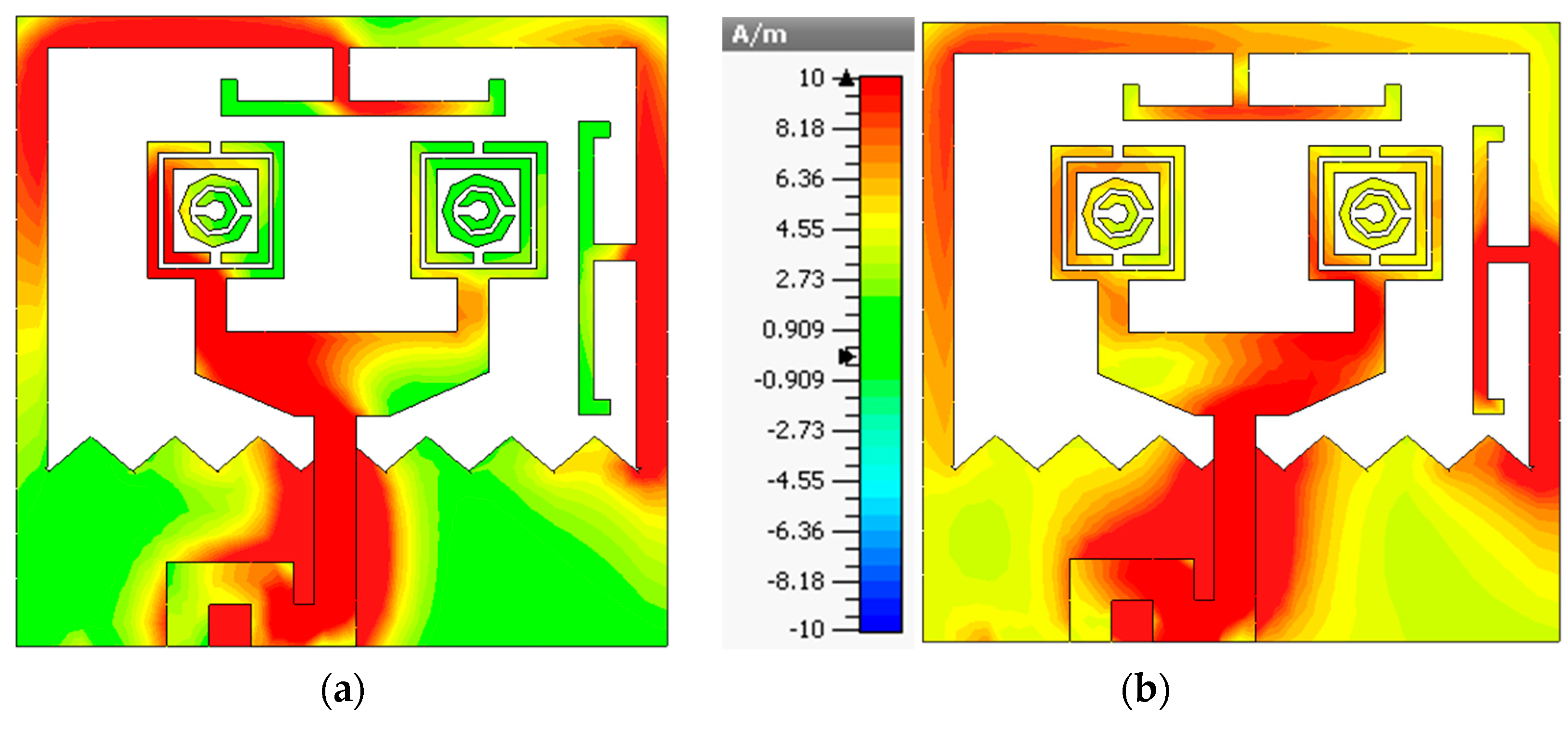
To understand the antenna’s performance, induced surface current distributions at 2.50 and 3.50 GHz are shown in
Figure 14a,b. The antenna patch structure is radiation sources because the surface current forms on them and current is related to the magnetic dipole (
) and electric dipole (
) moments of the resonator by the following relationships,
The intensity of the current are highest at resonance points, whereas the stop bands are creating by minimizing the current flowing through opposite direction. In
Figure 14a the surface current distribution neighboring split ring resonator (SRR) with the feed line in a dominant figure. The flows of current in the slotted SRRs were inversed to the current flow in the outward edges of the radiator patch and ground. In
Figure 14b, at 3.50 GHz the surface current was well distributed on SRRs, the area of microstrip feed line and the defected ground plane. The density of current is expressed by intensity of color. Due to the skin effect, current must cover curvier paths than a straight one in lower frequency. At higher frequency, the current flows through the surface of the conductor instead of the fundamental part. However, due to flow in opposite direction in the same metallic strips of the inner and outer ring resonators, which causes the stop band by nullifying the opposite current each other. The colors show the direction and intensity of surface current.
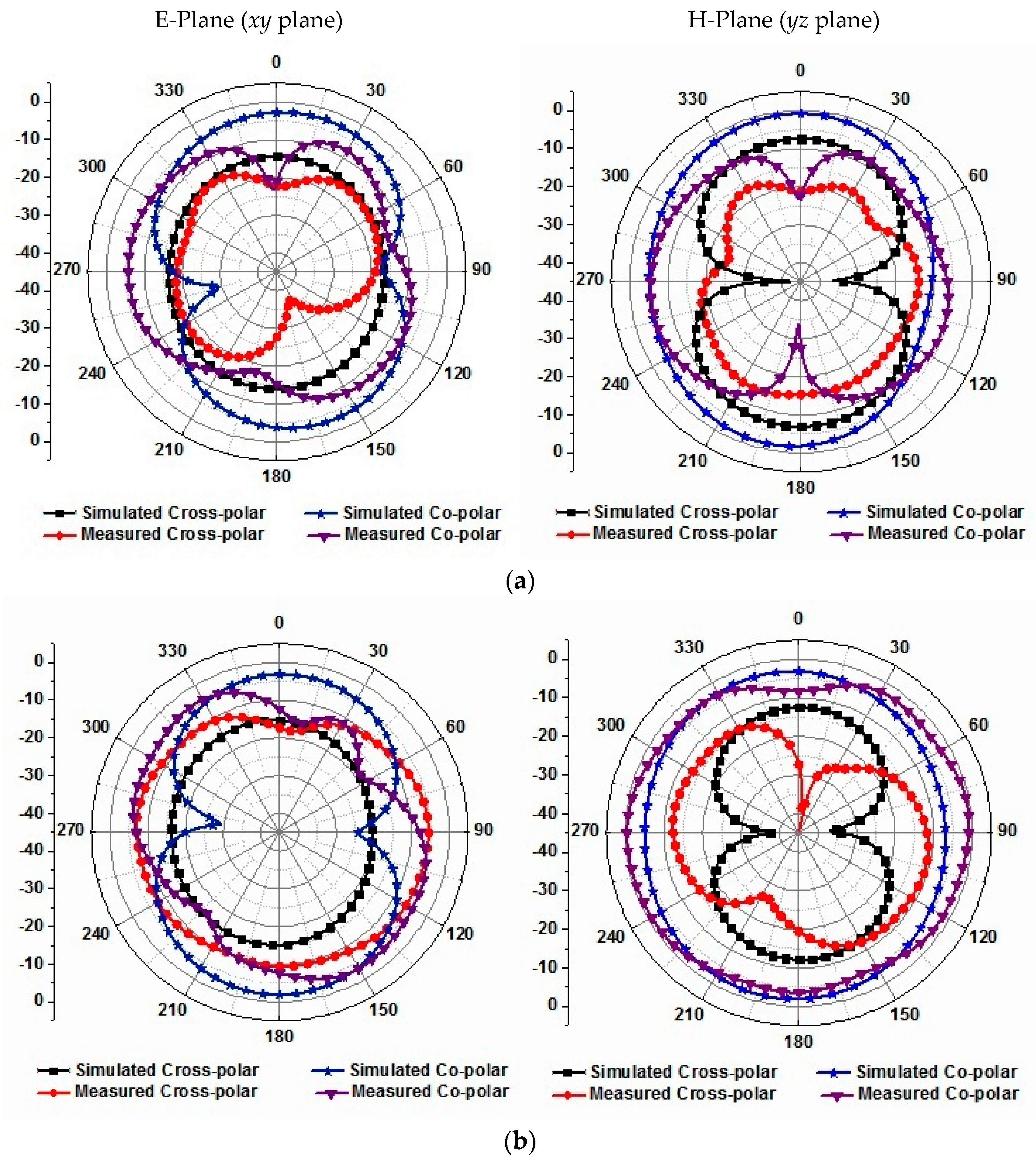
The radiation patterns of antenna were simulated at H-plane (
yz-plane) and E-plane (
xy-plane). The simulated and measured radiation patterns in case of co-polarization and cross-polarization in E-plane and H-plane were compared in
Figure 15a,b. ‘
Eθ’ represents the co-polarization and ‘
Eφ’ represents the cross-polarization. The co-polarization was greater than the cross-polarization in both E-plane and H-plane. The antenna tends to radiate energy equally to all direction. The measured radiation pattern demonstrated that at 2.47 GHz, the current was well distributed over the patch antenna plate and radiation patterns were nearly omnidirectional. However, at 3.62 GHz, the current was concentrated near the slots, thus the fields radiated mainly through the slots. Moreover, better radiation patterns depend primarily on accurately positioning the probe, eliminating distortions in the field introduced by the room, track or probe itself.
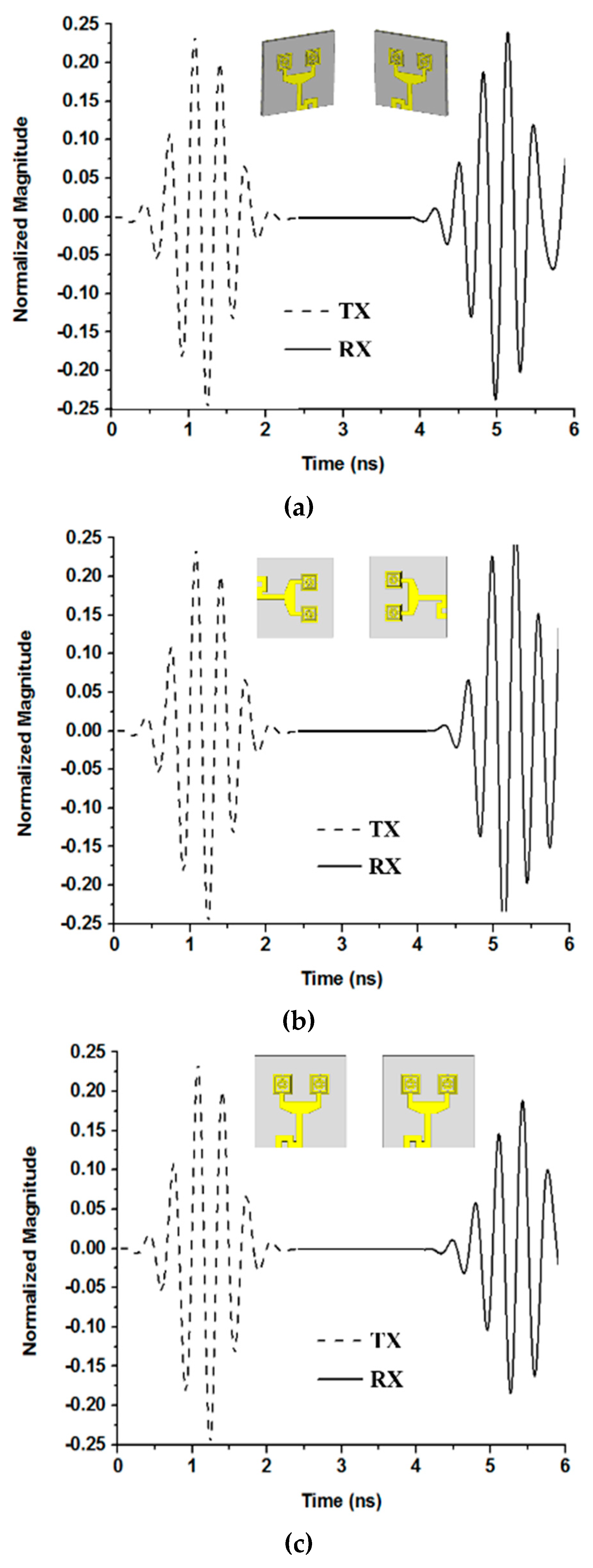
To investigate the proper communication performance of the proposed metamaterial inspired antenna time domain performance was analyzed, where one antenna used as a transmitter and another as a receiver. The fidelity parameter was used to estimate the signal distortion and Equation (15) was used to calculate the fidelity factor (
F).
where,
s(
t) and
r(
t) are the input and received pulses. Gaussian pulse is sent from broadcasting antenna to the receiving antenna. These two metamaterial inspired antennas have been exposed in distance of 10 mm in three different positions.
Figure 16a–c shows the transmitted and received signal at three different orientations (face to face, side by side X and side by side Y). By using Equation (15), the determined fidelity factor sequentially for the antenna face to face orientation in
Figure 16a was 0.86, antenna side by side X orientation in
Figure 16b was 0.92 and antenna side by side Y orientation in
Figure 16c iwas 0.89.
Table 4 represents a performance comparison in terms of antenna size, bandwidth, gain and applications between the proposed metamaterial embedded antenna and the existing antennas. In the table, the proposed metamaterial antenna has overall 31 × 30 mm
2 dimensions that are compact in size in comparison to all the reported antennas in [
9,
10,
11,
12,
13,
14,
15]. In Reference [
9] the antenna size is bigger than all and applicable for GSM frequency bands. The designed metamaterial embedded antenna has the total bandwidth of 220 MHz (2.38 to 2.60 GHz) and 390 MHz (3.40 to 3.79 GHz), whereas in References [
15,
16], the antennae had larger bandwidth but single band as well as applicable for only WiFi, WiMAX and WiMAX applications, respectively. Moreover, the gain of proposed metamaterial antenna was 2.25 dBi while in References [
10,
18] the antennae had larger gain 3.59 and 2.95 dBi but applicable for Bluetooth, WiMAX and WiFi, WiMAX applications. References [
9,
13] show quad frequency band, but are applicable for sequentially GSM, WLAN, and RFID applications. Finally, after detail investigation of existing antennae the proposed metamaterial antenna is compact in size, larger bandwidths, high gain and applicable for Bluetooth (2.40–2.485 GHz) bandwidth of 85 MHz, WiFi (2.4 GHz), WLAN (2.40–2.49 GHz and 3.65–3.69 GHz) bandwidth of 90 MHz and 40 MHz, and WiMAX (3.40–3.79 GHz) bandwidth of 390 MHz applications.

 ,
, 


