Abstract
In this paper, a new pulse width modulation (PWM) scheme using an offset function to reduce switching loss in the five-level H-bridge T-type inverter (5L-HBT2I) is proposed. The proposed modulation technique is implemented with a third harmonic offset voltage function. A new control voltage, that is adding the offset voltage into the initial control, is shifted to the top or bottom position of the carrier, simultaneously—where the absolute value of its load current is high or medium in comparison to other phase load currents. Due to reducing the intersection between a control voltage and the carriers, the number of switch commutations of the inverter is reduced. As a result of reducing the number of commutation count with a high current at the non-switching position, the switching losses of the inverter are decreased. Analysis and comparison of switching losses on the two-level and three-level inverters, which are components of 5L-HBT2I are presented. The power loss analysis on the 5L-HBT2I is performed. The proposed technique implements the switching loss reduction strategy based on setting the operation of the two-level inverter in six-step mode. PSIM software is used to clarify the proposed technique. The simulation results show that the total switching losses of the proposed technique in 5L-HBT2I reduce in comparison to the conventional sine PWM technique. A prototype is built to validate the proposed scheme. Simulation and experimental results match the analysis.
1. Introduction
Five-level inverters are power electronic converters that play important roles in applications of mechanical-electrical systems, transportation, power quality management, renewable energy conversion system, and motor drives [1,2,3,4]. In the design of five-level inverters, different topologies have been evolved, including the diode-clamped [5,6,7,8,9], flying capacitor [10,11,12,13], cascaded H bridge [14,15,16], and T type topologies [17,18,19,20]. A new single-phase five-level T-type inverter can reduce the harmonic components compared with that of the traditional full-bridge three-level PWM inverter under the same conditions of DC voltage source and switching frequency [18]. In [19] the DC-DC boost converter is connected to a five-level inverter and PI control is used, to control the inverter with much less total harmonic distortion (THD) and near unity power factor. To enhance the input voltage, three PV strings in cascade and parallel configurations with the five-level inverter are found in [19]. To maintain the power factor at near unity, the inverters in [19] and [20] use a proportional–integral (PI) current control scheme. The main solutions for the small-scale rooftop PV applications are proposed in [20]. That paper presents a comparison of four multilevel converters based on the T-type topology.
The switching loss is very important to evaluate the performance of the inverter, especially when multilevel inverter operates at a high frequency. Several studies on switching loss reduction have been introduced in recent years [21,22,23,24,25,26]. The complete analytical calculation of the switching loss is proposed in [23] for the basic inverters. The switching losses of the IGBT depend on switching frequency, load current, input DC voltage, and characteristics of switches are presented in [24]. The paper [24] shows that the total switching losses of the inverter on a control voltage period are proportional to switching frequency, load current, and DC voltage supply. The switching frequency depends on the carrier frequency and the modulation method. Note that the switching frequency is opposite to the total harmonic distortion (THD) of the output voltage. So that, lower carrier frequencies based switching loss reduction can increase THD value. Therefore, a new technique for switching loss reduction without THD increment is needed to be solved. As a result, the switching energy of the switches when the switches operate is turned on (Ec(on)) or turned off (Ec(off)) mode, are determined by current and voltage across the switch (IC and VCE) [25].
The average switching loss in the switch (PS) during each period Ts is calculated as Equation (1) [25].
where:
- fs—switching frequency
- VCE—voltage across the switch when the switch is turned off
- Von—voltage across the switch when the switch is turned on
- Is—current through the switch when the switch is turned on
- tc(on)—turn-on cross-over interval
- tc(off)—turn-off cross-over interval
From Equation (1), it can be seen that to reduce switching losses it needs to reduce switching frequency (fs). Or for reduction switching loss, it needs to choose a switching state based on IC and VCE of phase to have the smallest value in the three-phase. As a result, fs, IC and VCE are three basic elements that affect to reduce switching loss. A new space vector modulation strategy with two PI regulators is used in both DC voltage and load voltage sides for controlling the PWM parameters. So, the non-switching state can be controlled by these parameters to generate pulses as found in [26]. The switching losses are reduced by reducing either switching frequency or instantaneous current and voltage values at the time of switching in [26]. Since using two PI regulators, the control technique is very complex and hard to control for the system.
A reduced switching loss PWM strategy to eliminate common mode voltage in multilevel inverters is presented in [27]. This PWM method has increased switching times for the phase with the smallest load current by comparing the three-phase load current to eliminate common mode voltage. Simulation and experimental results in [27] are performed based on the standard models with the collector-emitter voltage of the IGBTs equaled. Therefore, for application to other models, which the voltage crossed IGBTs is not the same, as if the 5L-HBT2I, its effect of loss reduction may not be very high. The two modified space vector modulation strategies were proposed in [28] for the reduction of the qZSI number of switch commutations at high current level with shorter periods during the fundamental cycle, i.e., reducing the switching loss, simplifying the generation of the gate signals by utilizing only three reference signals, and achieving a single switch commutation at a time were also presented in [28].
This paper proposes a new modulation technique to reduce the number of switch commutations for switching losses reduction. There is no switching on the phase which the control voltage has the smallest displacement to top or bottom of the carrier, and the absolute of the load current being the first or second large. In addition, reducing turn on and off the switch that has a large across voltage, will be done to reduce switching losses. The paper is organized as follows: in Section 2, the topology, operating principles, and circuit analysis of the three-phase 5L-HBT2I are presented. Section 3 presents switching loss calculation for 5L-HBT2I. Section 4 presents the proposed PWM scheme. Simulation and experimental results are shown in Section 5. Finally, the result is summarized in Section 6.
2. Three-Phase Five-Level H-Bridge T-Type Inverter Topology
Figure 1 shows the three-phase 5L-HBT2I. As shown in Figure 1a, the 5L-HBT2I consists of three DC sources (Ua, Ub, Uc), six capacitors (Ca1, Cb1, Cc1, Ca2, Cb2, and Cc2), and three T-type H-bridge circuits.
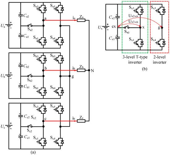
Figure 1.
Five-level T-type H-bridge inverter topologies. (a) Three-phase inverter and (b) One phase module.
Define TSxi is status of the ith switch on phase x (x = a, b, c); where i is the index of switches (1 to 5), with conditions:
Figure 1b shows a structure of phase x, where a leg of 5L-HBT2I is built from two single-phase inverters: two-level and three-level T-type.
From Equations (3) and (4), the pole voltage of two-level (Ux2-cx) and three-level T type inverter (Ux3-cx) are determined:
Hence, the voltage from phase to pole (Uxg) is determined as
Set TSx is status of phase x:
So, the phase to pole voltages is given as Equation (9).
The output phase and line-to-line voltages of this inverter is given as Equations (10) and (11).
As a result, the third order harmonic does not appear in the output phase voltage (Vxn), while it appears in both pole voltage (Vxg) and line-to-line voltage. Therefore, the proposed algorithm has offset the function at the third order harmonic, which will not affect the third order harmonic magnitude of the load. From Equation (8) to Equation (11), the values of Vxg can be determined in Table 1. As shown in Table 1, the pole voltage Vxg has five levels including two positive, two negative, and one zero.

Table 1.
Switching state of five-level H-bridge T-type inverter (5L-HBT2I) for phase-x index.
3. Switching Loss Calculation for 5L-HBT2I
The switching loss depends on the load current and collector-emitter voltage of the power switches and the number of commutations during the entire fundamental cycle [24,25]. Therefore, the switching losses of the 5L-HBT2I will be calculated based on the switching losses of the power switches of each phase, where phase x consists of five switches: Sx1–Sx5, x = a, b, c.
Figure 1b and Table 1 can be seen that
where VCE,i is the voltage across switch Sxi when Sxi is turned-off (i = 1, 2, 3, 4, 5).
And the current through switches, is is determined as
In Equation (13), iSi and iLx are current through switch Sxi when Sxi is turned-on (i = 1, 2, 3, 4, 5) and the load current over phase x (x = a, b, c), respectively.
Hence, the average value of the local (per control voltage cycle) switching loss over switches Sx1–Sx5 (for instance, for phase-a) can be calculated as [27]
Similarly, we have
where PSi is an average value of the local (per carrier cycle) switching loss over the switch (i = 1, 2, 3, 4, 5). Von,i is voltage across switch Sxi in turned-on state.
Equations (14)–(18) can show that switching loss decreases if the switching is on the phase, which has a small load current. Due to the decrement of the number of commutations on two-level inverter switches (Sx5 or Sx4), the switching loss will be smaller when compared with three-level T-type inverter switches (Sx1 or Sx2 or Sx3).
As a result, the proposed technique helps to reduce the switching loss by reducing the number of commutations on the phase, which has the absolute of the load current are first or second large in three-phase and by reducing the number of commutations on two level inverter.
4. Proposed Algorithm
4.1. Principle of the Proposed Algorithm
The switching loss depends on the current through power switches, the voltage across the switch, and the number of commutations in the period of control voltage is shown in Equations (14)–(18). Since the switching loss can be decreased by reducing switching frequency of Sx5 and Sx4 and reducing the number of commutations on the phase, which has the absolute of the load current is high or medium in comparison to another phase. Therefore, in the first stage, the new control voltages are determined with a non-switching state on the phase, which has the smallest displacement to top or bottom peak (of the carrier) and the absolute of the load current being the first or second largest. In addition, in the second stage, the control voltages that have been determined in the previous stage, are divided into the control voltage for the two-level inverter and three-level T-type inverter for reducing switch turn-on/turn-off on the two-level inverter.
The first stage:
It is defined that vx is the initial control voltage phase x (x = a, b, c) and vrx is control voltage that it is determined as the new control voltage by adding voffset into vx from first stage of proposed algorithm. The maximum ampplitude of carrier is selected by 1. Due to the 5-level inverter, threshold comparison of the carrier is 0, 1, 2, 3 and 4. The initial control voltage of phase vx is determined as Equation (19).
where vx, m, ω and θ0x are the initial control voltage of phase x, modulation index, angular velocity, and initial phase angle, respectively.
The error of vx and Lx are determined:
Call IxABS is the absolute of current across phase x, then
where θ is phase angle, ILx is the load current of phase x (x = a, b, c).
The maximum, minimum, medium of error (emax, emin, emed) and the maximum and medium of absolute of load current (Imax, Imed) are defined:
Case 1: When the ixABS is the largest and (ex = emin) or (ex = emax), the none switching phase is x and the offset voltage (voffset) is determined through the value ex as Equation (25)
Case 2: When iaABS is the largest and ea equal the emed, for reducing error of output voltages, the offset voltage will be not equal to ea. In this case, another phase has the absolute of the load current as medium (assuming it is phase b) and the error (eb) of vb and Lb fix the maximum or minimum. Then, the offset voltage is calculated following ibABS and eb as Equation (26)
Table 2.
The offset voltage of the 5L-HBT2I.
If the matrixes from Equation (27) to Equation (31) are defined, the offset voltage will be calculated as Equation (32).
The new control voltage vrx is determined
Since matrixes [], [], [], [ and [] have “0” and “1” values, which can be determined by simple comparison commands lead to the calculation of the offset voltage easy and quick. The new control voltage (vrx) is the old control voltage (vx) add the offset voltage. The new control voltages (vrx) on the phase which the absolute of the load current are first or the second large in three-phase and ex equal emax or emin will be shifted to the top or bottom peak of the carrier.
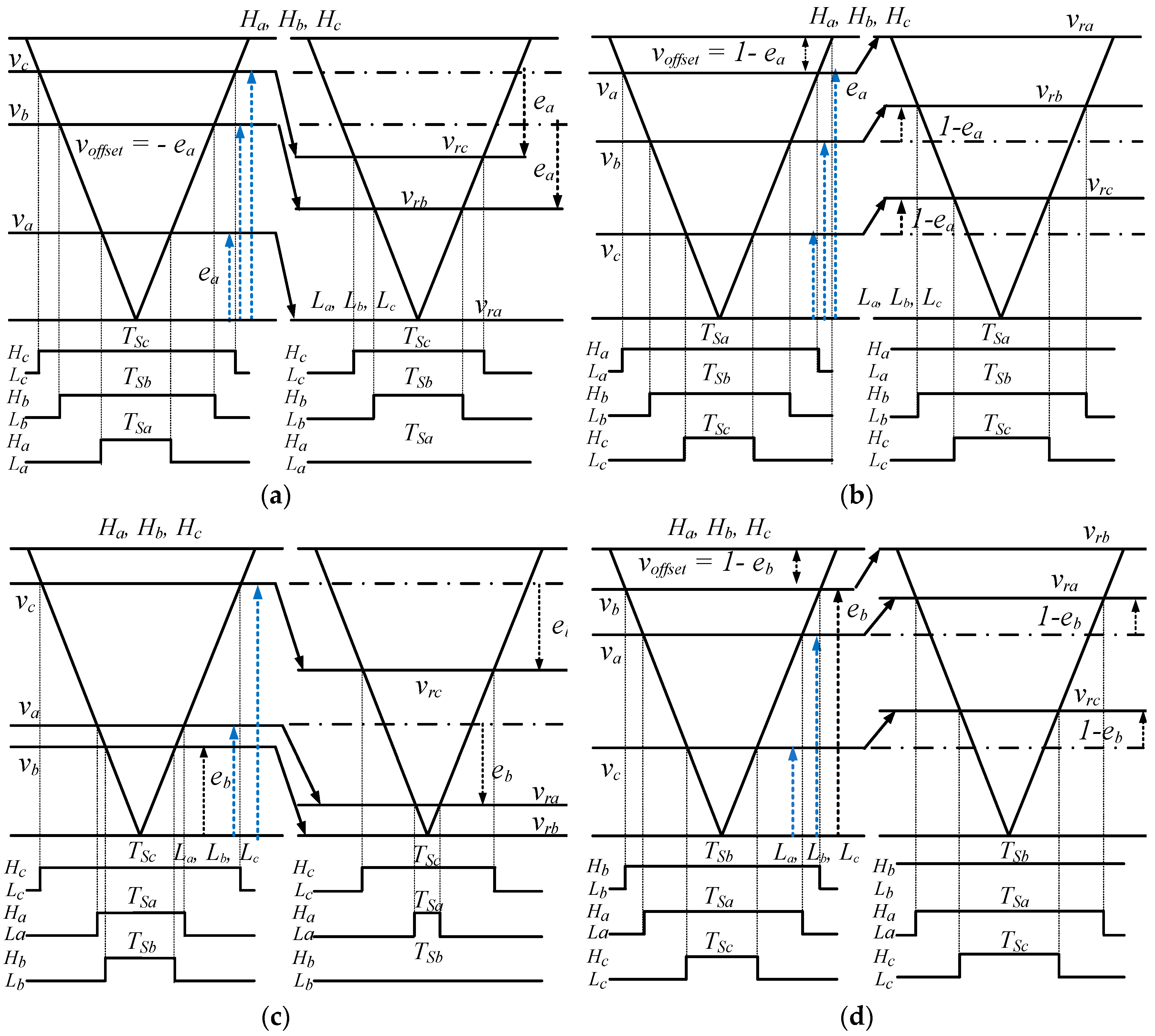
Figure 2 shows the shift of the control voltages according to the conditions of the proposed algorithm. As shown in Figure 2a, when , the offset voltage is −ea. This offset voltage is added to the original control voltages so the new control voltages will shift down to the new positions. The new position of the control voltage of phase-a will be La. Therefore, there will be no switching on the phase-a when as shown in Figure 2b. Similarly, the switching state on the phase-b is off if , as shown in Figure 2c or Figure 2d.
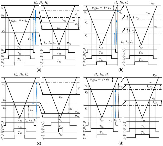
Figure 2.
Offset voltages under the proposed algorithm. (a) ; (b) ; (c) ; (d) .
The second stage:
In the second stage, the control voltages that were created in the previous stage will be divided into the control voltage for the two-level inverter and three-level T-type inverter. Since the two-level inverter is operated in six-step mode, its control voltage can be calculated as
In addition, from Equation (7), it is easy to determine the control voltages for three-level T type, which are:
where vrx is the control voltage, created form first stage; vx,2l and vx,3l are the control voltages for two-level inverter and T-type inverter on phase x.
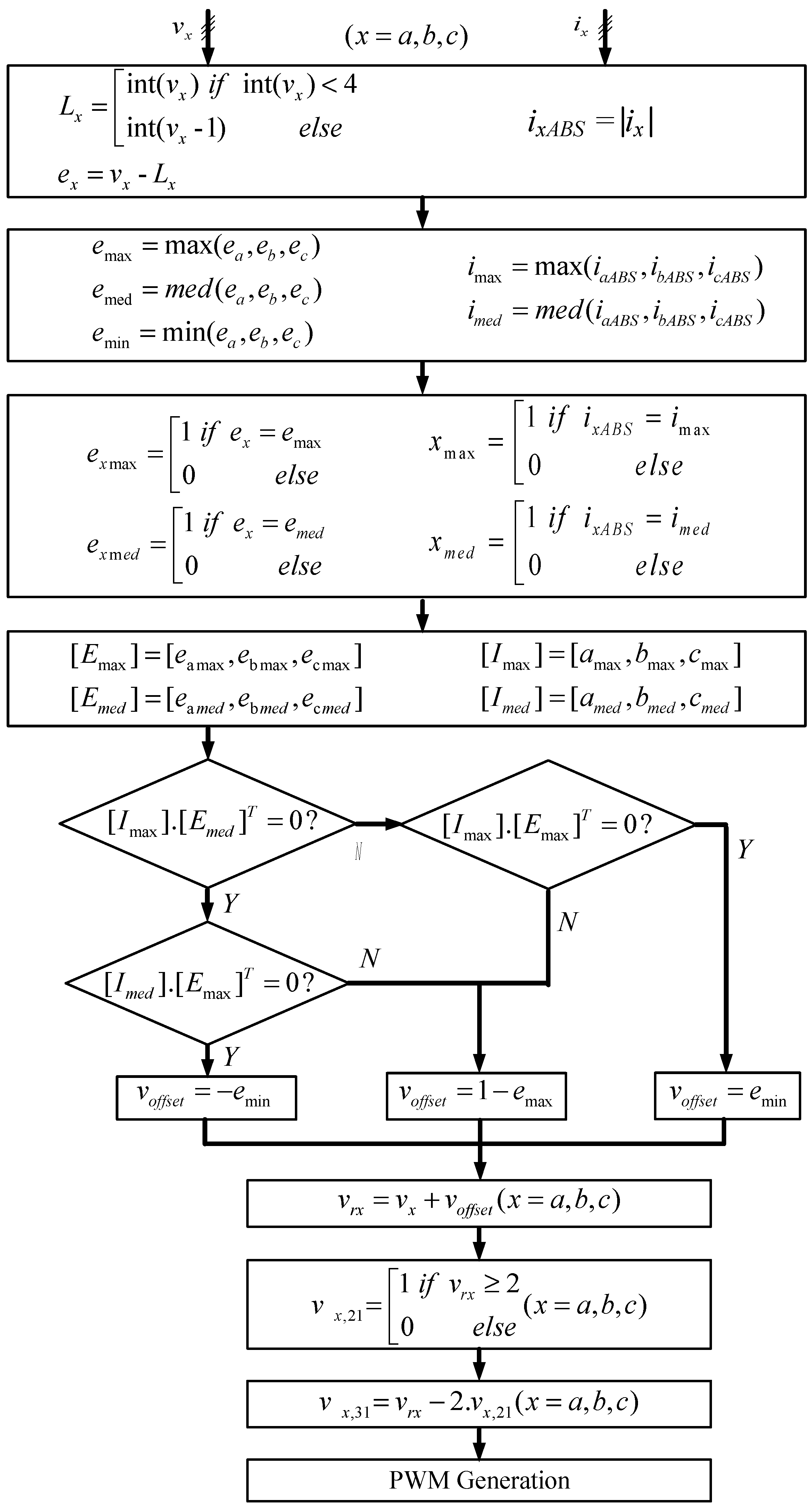
4.2. Flow Chart
Figure 3 shows a flow chart of the proposed algorithm using simple commands such as subtraction, and comparison on the program. The comparison of the phase currents can be done by comparing hardware circuits that do not require the use of expensive sensors. Thus, calculation time of the algorithm is low and suitable for closed-loop control or other control methods.
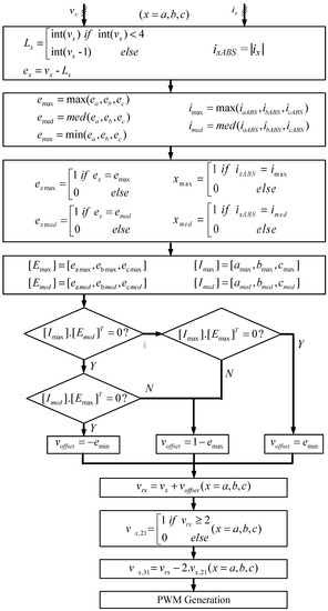
Figure 3.
The flow chart of the proposed scheme.
For example, assuming that control voltages va, vb, and vc are 1.12 V, 0.64 V and 3.24 V, respectively, from Equation (22), the error of vx and Lx are . From Equation (24), .
Assuming that IaABS > IbABS > IcABS, from Equations (27) and (28), . From Equations (30)–(32), . From Equations (22)–(32), the offset voltage is . Then, new control voltages are
When vra = 1 V, switches S1, S3, and S5 are turned off while switches S2 and S4 are turned on. Thus, the phase-a switches will not be switched in one cycle T. Similarly, when vrc = 3.12 V, S1, S3, and S4 are turned off while S2 and S5 are switching. As a result, the phase-c switches will be switched in one cycle T. Therefore, the proposed algorithm can reduce the switching times of the switches.
5. Simulation and Experimental Results
5.1. Simulation Results
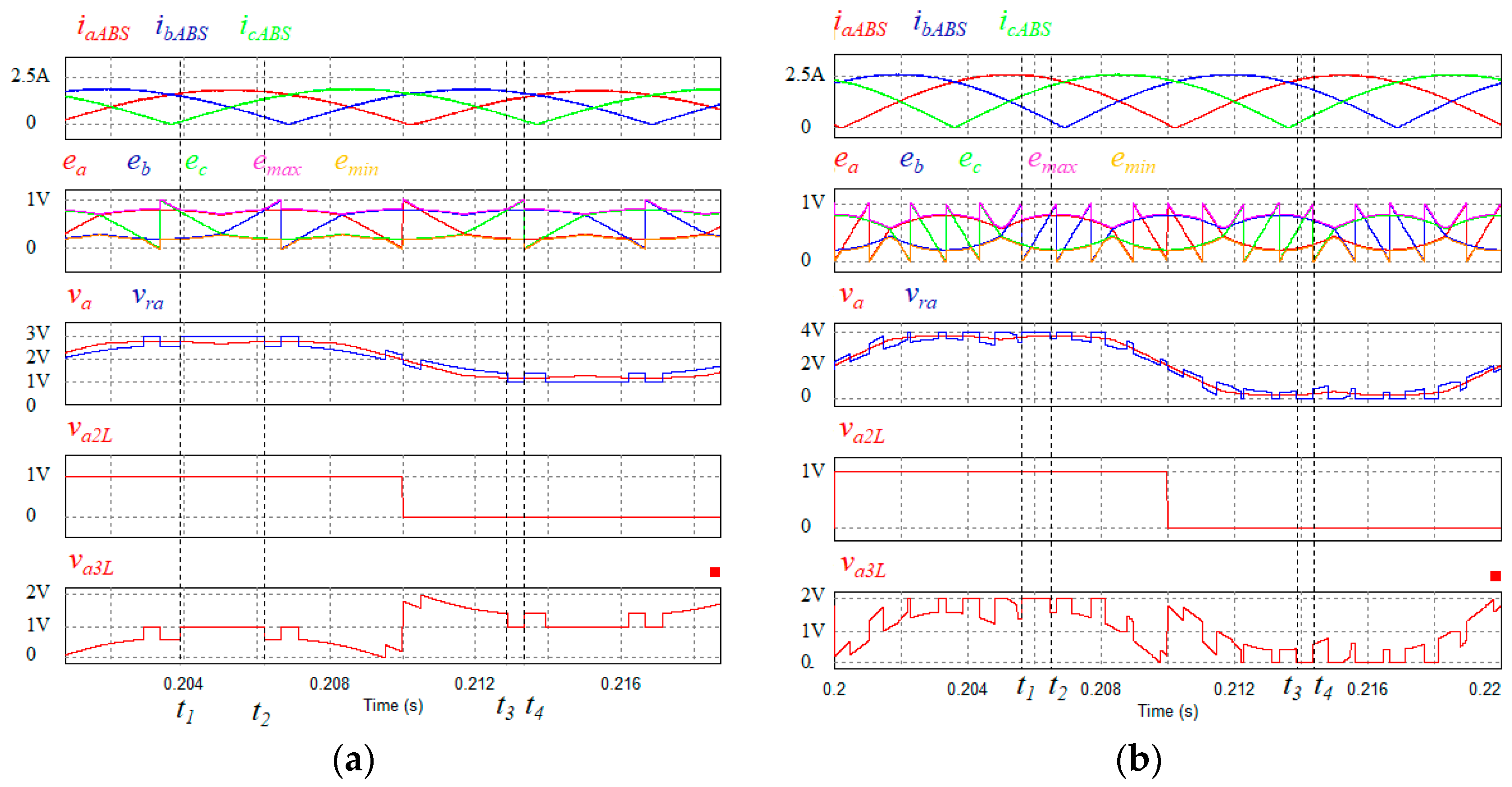
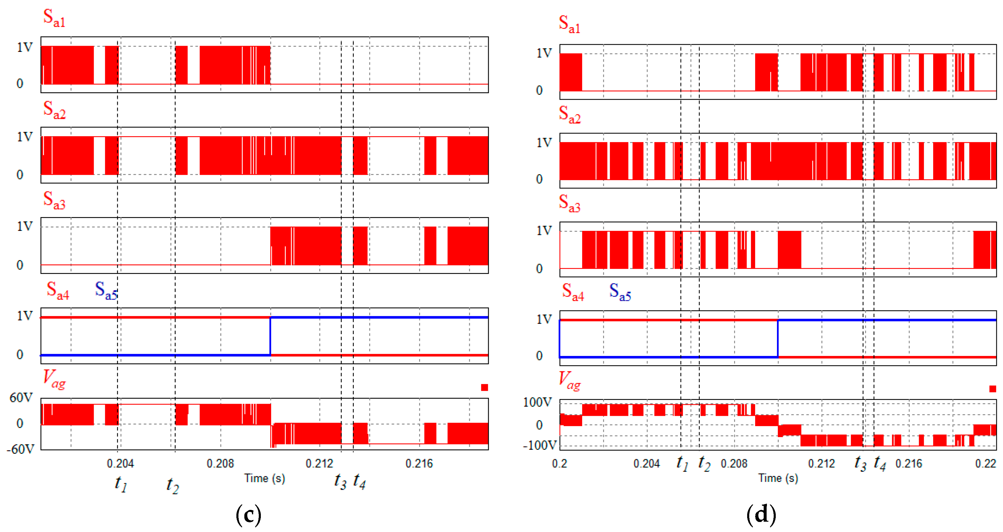
Parameters used in simulation is shown in Table 3. Figure 4 shows the simulation results of the proposed algorithm when modulation index are 0.4 and 0.9, respectively. The waveforms from top to bottom in Figure 4 are three-phase absolute current, three-phase error (ea, eb, ec), maximum and minimum errors (emax and emin), the initial voltage (vx) and new control voltage (Vrx), control voltage of two-level inverter (va2L), and control voltage of three-level T-type inverter (va3L), the next waveforms are gating signals of Sx1 to Sx5 and the bottom is the pole voltage output. It can be seen that from t1 to t2, iaABS is maximum and ea hit maximum (emax), then voffset will be 1 − ea lead to the control voltage of phase a move up to 3V; see Figure 4a and obtain 4V; see Figure 4b. As shown in Figure 4a, during a time interval of [t1 to t2], the control phase-a voltage is 4 V. As a result, the switching states on phase-a are (S5a = 0, S4a = 1, S3a = 1, S2a = 0 and S1a = 0) and its phase pole voltage is = 100 V. Similarly, in Figure 4b, the phase-a to pole voltage is = 50 V when (S5a = 0, S4a = 1, S3a = 0, S2a = 1 and S1a = 0). From t3 to t4, ibABS is maximum, the eb is medium. Simultaneously, the absolute of phase a current load (iaABS) is medium and ea is emin as analyzed in the above section, the offset voltage is –ea and the new control voltage of phase a shift down 0 V (m = 0.9) and 1 V (m = 0.4), so there is no switching in phase-a. Similarly, the phase-b and phase-c in the situation have no switching.
Table 3.
Parameters used in simulation.
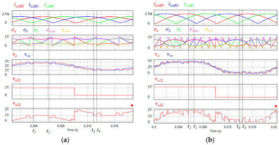
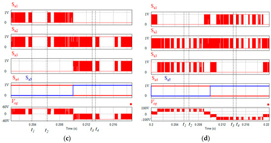
Figure 4.
Control voltage generation, gating signals of Sa1 to Sa5 and the phase pole voltage in the proposed technique with (a,c) m = 0.4 and (b,d) m = 0.9.
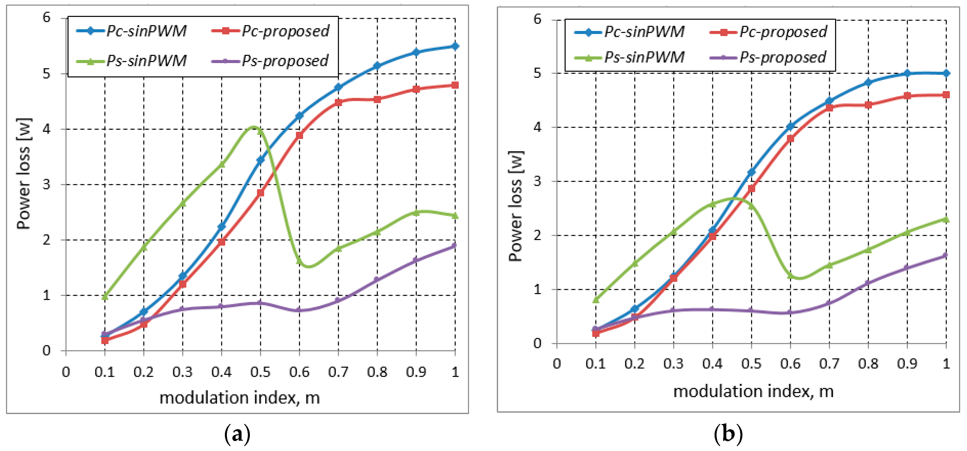
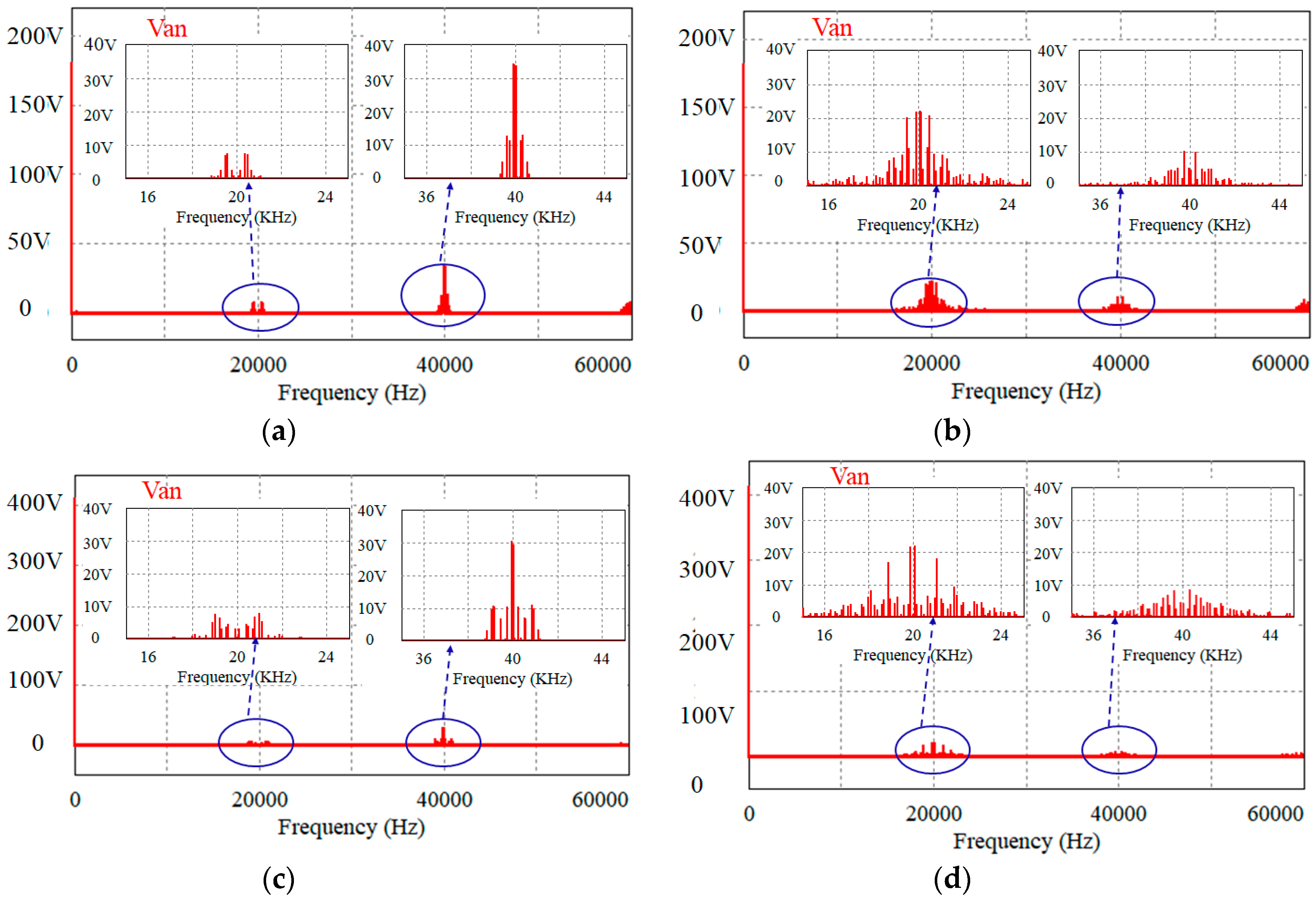
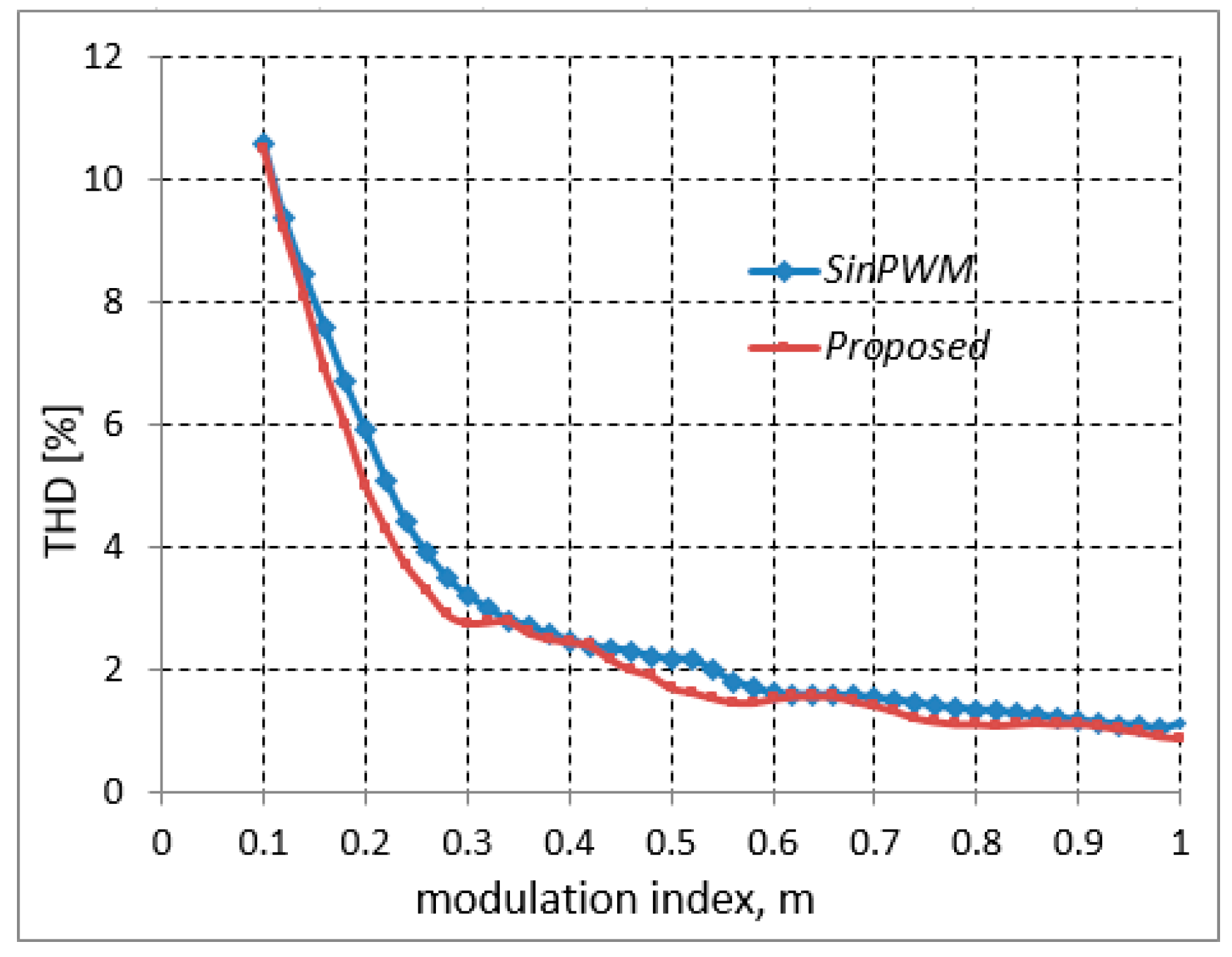
To evaluate the efficiency of switching loss reduction, IGBT CM1000HA-24H module (Mitsubishi Electric., Tokyo, Japan) in PSIM’s device database is used in the simulation. Figure 5 shows the conduction loss (Pc-sinPWM), switching loss (Ps-sinPWM) using sine PWM algorithm and conduction loss (Pc-proposed), switching loss (PS-proposed) using the proposed algorithm on a phase on changing carrier frequency. As a result, the proposed technique can reduce switching losses. The switching loss reduction value is maximized when m = 0.5, equivalent to 78% reduction. There is no significant difference in conduction loss (Pc) between the proposed algorithm and sinPWM algorithm, especially at low carrier frequencies. The difference in conduction loss is due to the difference in the high harmonic amplitude between the proposed algorithm and sinPWM algorithm. When the carrier frequency is not high enough (e.g., at fc = 5 kHz), the load phase voltage that applies the proposed technique has the high harmonic amplitude at some modulation index values. Therefore, the conduction loss in this case is greater than that in the sinPWM method as in Figure 5c,d. The harmonics spectrum of the proposed and sinPWM algorithms are presented in Figure 6. The harmonics with a large amplitude in the proposed technique focus around the carrier frequency, while they are around twice the carrier frequency in the sinPWM algorithm. The THD of the phase current in the two algorithms is slightly different, as seen in Figure 7.
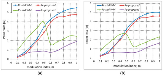
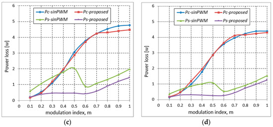
Figure 5.
Power loss on a phase under sinPWM method and proposed algorithm at carrier frequency of (a) 20 kHz, (b) 15 kHz, (c) 10 kHz, and (d) 5 kHz.
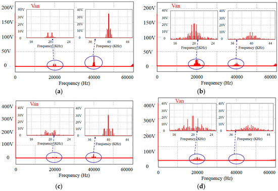
Figure 6.
Harmonics spectrum of phase voltage at fs = 20 kHz using (a) sinPWM method with m = 0.4, (b) proposed method with m = 0.4, (c) sinPWM method with m = 0.9, and (d) proposed method with m = 0.9.

Figure 7.
Total harmonic distortion (THD) comparison between sinPWM method and proposed technique at fs = 20 kHz.
Figure 7 shows a comparison of THD values of the phase current between sinPWM method and the proposed technique. As shown in Figure 7, THD value of the phase voltage of 5L-HBT2I under the proposed algorithm is smaller than that with the sinPWM method at fc = 20 kHz. This can explain that the two-level inverter only operates in a six-step mode with rarely rapid changes of phase voltage on this inverter. As a result, the output harmonics have a small amplitude and conductive losses are also lower than sinPWM techniques, as shown in Figure 5.
Under the load of 40 Ω and 10 mH at the output frequency of 50 Hz, the calculated load power factor is 0.997. Table 4 shows the power factor (PF) and the power factor displacement (PFD) in simulation. As shown in Table 4, the simulated power factor of the inverter is lower than the calculated load power factor of 0.997. This is due to the harmonics distortion of load current and voltage.
Table 4.
Simulated power factor and power factor displacement.
5.2. Experimental Results
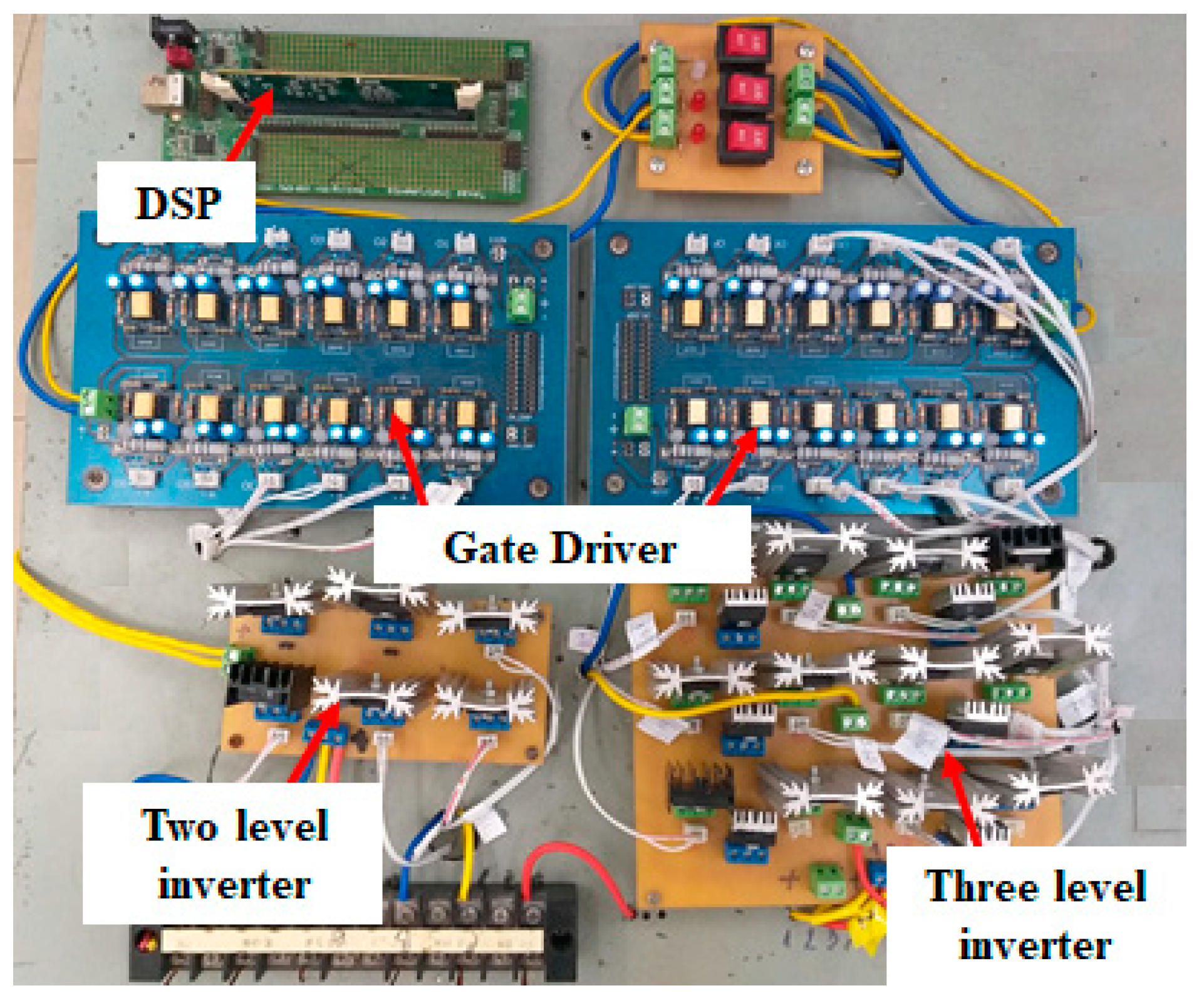
An experimental model based on the DSP TMS320F28335 microcontroller (Texas Instruments, Dallas, TX, US) is built in the laboratory to verify the effectiveness of the proposed control technique with the elements in Table 5. Figure 8 shows a laboratory prototype. The input voltage is 100 V. The output frequency is 50 Hz, while the switching frequency of the inverter circuit is 5 kHz. A three-phase inductive load of 40 Ω and 10 mH is used in the experiment.
Table 5.
Elements used in experiment.

Figure 8.
Experimental setup of the prototype.
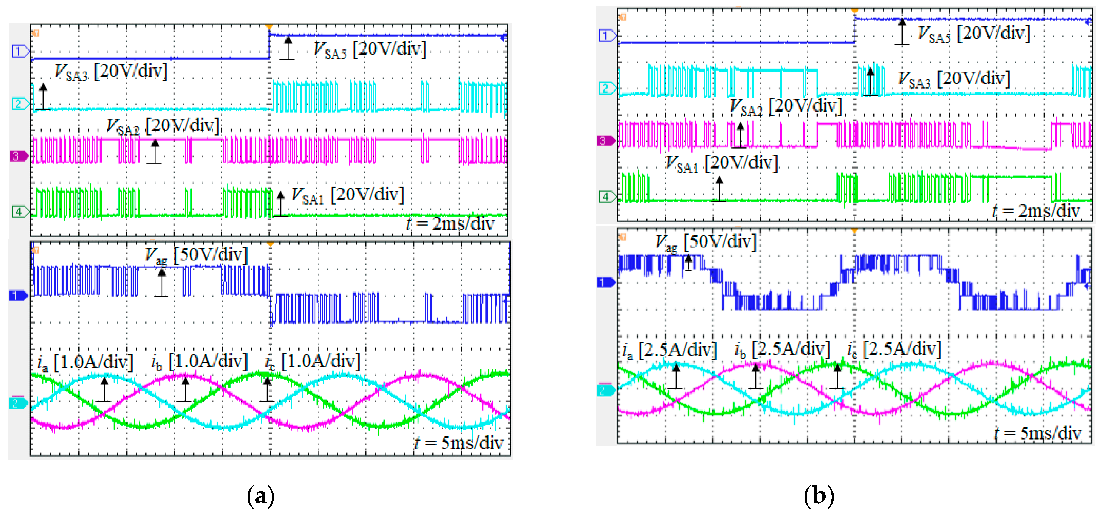
Figure 9 shows the experimental result of the proposed algorithm when m = 0.9 and m = 0.4. In Figure 9, the waveforms from the top to the bottom are the gating control signals of the power switches SA5, SA3, SA2 and SA1, the pole voltage (Vag), the phase voltage that its harmonic spectrum is in Figure 10. The experimental result of the proposed algorithm in Figure 9 are under modulation index m = 0.4 (Figure 9a) and m = 0.9 (Figure 9b).
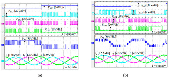
Figure 9.
Experimental results at (a) m = 0.4 and (b) m = 0.9.
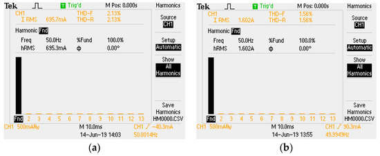
Figure 10.
The load current fast Fourier transform (FFT) and its THD. (a) m = 0.4 and (b) m = 0.9.
The experimental results are close to the simulation results. Figure 9a,b show the position “no switching” in the phase, which has the absolute of its load current hitting maximum or medium in three phases. The gating signal of SA5 is similar to that of SA4, that is the switch of the two-level inverter. This is similar to its waveform in the six-steps mode.
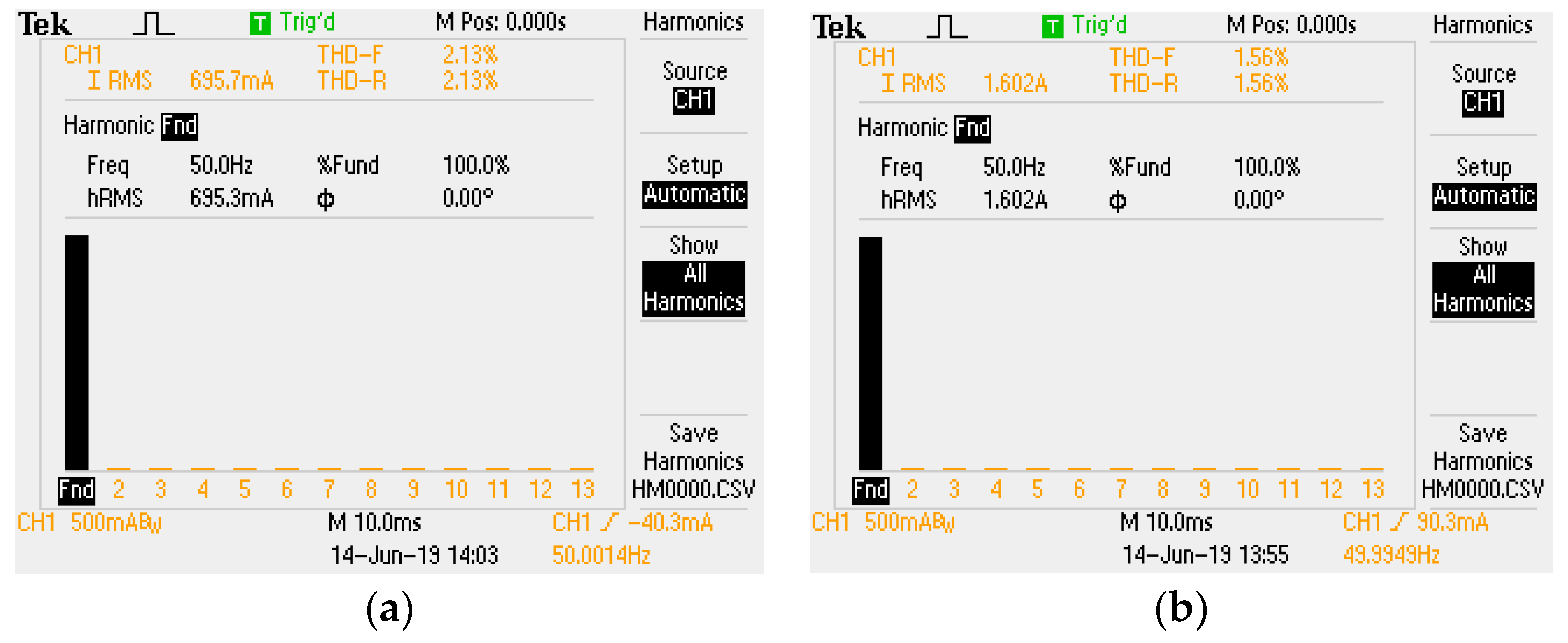
Figure 10 shows the experimental results of the load current fast Fourier transform (FFT) and its THD at m = 0.4 and 0.9. The experimental results are close to the simulation results. As shown in Figure 10, the THD of the load current with the proposed algorithm at m = 0.4 is bigger it at m = 0.9. Since the THD of the load current under the proposed algorithm is smaller than 5%, this complies in the standard IEC61000-4-30 Edition 2 Class A. The experimental results in Figure 10 show that the amplitude of lower harmonics is very small. That is one of the advantages of the proposed technique. The measured THD values in Figure 10 are close to the simulation results shown in Figure 7.
6. Conclusions
The paper presents the carrier based PWM algorithm for 5L-HBT2I by using the offset function to reduce the number of commutations on the power switches. Since the phase leg switches are reduced, the number of commutations at maximum phase current are absolute, the two-level inverter in 5L-HBT2I is on six-step mode, and the switching losses of the inverter 5L-HBT2I are reduced under the proposed algorithm. The switching loss reduction value, in the proposed algorithm for 5L-HBT2I, is maximized when m = 0.5, that is equivalent to a reduction of 78%. Since there is no increase conductive loss when applying the proposed algorithm on 5L-HBT2I, the power loss of the inverter is also reduced. Due to no increase of THD, this algorithm not only reduces the number of commutations but also hits ME standards as IEC61000-4-30 Edition 2 Class A at small modulation indexes [28].
Author Contributions
This paper was a collaborative effort among all authors. All authors conceived the methodology, conducted the performance tests and wrote the paper.
Funding
This research was funded by KC 186 project.
Acknowledgments
This work was supported by the Advanced Power Electronics Laboratory, D405 at Ho Chi Minh City University of Technology and Education, Viet Nam.
Conflicts of Interest
The authors declare no conflict of interest.
Nomenclature
| 5L-HBT2I | Five-level H-bridge T-type inverter |
| fs | Switching frequency |
| NA | Not applicable |
| Pc-sinPWM | Conduction loss using sine PWM |
| Pc-proposed | Conduction loss using proposed |
| PI | Proportional integral |
| Ps-proposed | Switching loss using proposed |
| Ps-sinPWM | Switching loss using sine PWM |
| PV | Photovoltaic |
| PWM | Pulse width modulation |
References
- Bin, W.; Mehdi, N. High-Power Converters and Ac Drives; IEEE Press/Wiley: Hoboken, NJ, USA, 2016. [Google Scholar]
- Zhang, J. Modified cascaded multilevel grid-connected inverter to enhance european efficiency and several extended topologies. IEEE Trans. Ind. Inform. 2015, 11, 1358–1365. [Google Scholar]
- Baiju, M.R. Five-level cascaded multilevel motor driver for electrical vehicle with battery charge management. In Proceedings of the Power Engineering Conference, Sydney, NSW, Australia, 14–17 December 2008. [Google Scholar]
- Nallamekala, K.K.; Kalyan, U.M.; Sivakumar, K. Harmonic reduction technique with a five-level inverter for four pole induction motor drive. In Proceedings of the International Future Energy Electronics Conference (IFEEC), Tainan, Taiwan, 3–6 November 2013; pp. 482–487. [Google Scholar]
- Akagi, H. Multilevel converters: Fundamental circuits and systems. Proc. IEEE 2017, 105, 2048–2065. [Google Scholar] [CrossRef]
- Ye, Z.B.; Xu, Y.M.; Wu, X.; Tan, G.; Deng, X.M.; Wang, Z.C. A simplified PWM strategy for a neutral-point-clamped (NPC) three-level converter with unbalanced dc links. IEEE Trans. Power Electron. 2016, 31, 3227–3238. [Google Scholar] [CrossRef]
- Do, D.T.; Nguyen, M.K. Three-level quasi-switched boost T-type inverter: Analysis, PWM control, and verification. IEEE Trans. Ind. Electron. 2018, 65, 8320–8329. [Google Scholar] [CrossRef]
- Barros, J.D.; Silva, J.F.; Jesus, É.G. Fast-predictive optimal control of NPC multilevel converters. IEEE Trans. Ind. Electron. 2013, 60, 619–627. [Google Scholar] [CrossRef]
- Choudhury, A.; Pillay, P.; Williamson, S. DC-bus voltage balancing algorithm for three-level neutral-point-clamped (NPC) traction inverter drive with modified virtual space vector. IEEE Trans. Ind. Appl. 2016, 52, 3958–3967. [Google Scholar] [CrossRef]
- Abdelhakim, A.; Mattavelli, P.; Spiazzi, G. Three-phase three-level flying capacitors split-source inverters: Analysis and modulation. IEEE Trans. Ind. Electron. 2017, 64, 4571–4580. [Google Scholar] [CrossRef]
- He, L.; Cheng, C. A flying-capacitor-clamped five-level inverter based on bridge modular switched-capacitor topology. IEEE Trans. Ind. Electron. 2016, 63, 7814–7822. [Google Scholar] [CrossRef]
- Du, S.; Wu, B.; Zargari, N. Common-mode voltage elimination for variable-speed motor drive based on flying-capacitor modular multilevel converter. IEEE Trans. Power Electron. 2018, 33, 5621–5628. [Google Scholar] [CrossRef]
- Sayli, K.; Rohini, M.; Amarjeet, P. A 5-Level single phase flying capacitor multilevel inverter. Int. Res. J. Eng. Technol. (IRJET) 2017, 4, 348–352. [Google Scholar]
- Gadalla, A.S.; Yan, X.; Altahir, S.Y.; Hasabelrasul, H. Evaluating the capacity of power and energy balance for cascaded H-bridge multilevel inverter using different PWM techniques. J. Eng. 2017, 13, 1713–1718. [Google Scholar] [CrossRef]
- Malinowski, M.; Gopakumar, K.; Rodriguez, J.; Pe, X.; Rez, M.A. A Survey on cascaded multilevel inverters. IEEE Trans. Ind. Electron. 2010, 57, 2197–2206. [Google Scholar] [CrossRef]
- Nordin, N.M.; Idris, N.R.N.; Azli, N.A. Direct Torque Control with 5-level cascaded H-bridge multilevel inverter for induction machines. In Proceedings of the IECON 2011—37th Annual Conference of the IEEE Industrial Electronics Society, Melbourne, VIC, Australia, 7–10 November 2011; pp. 4691–4697. [Google Scholar]
- Shin, H.; Lee, K.; Choi, J.; Seo, S.; Lee, J. Power loss comparison with different PWM methods for 3L-NPC inverter and 3L-T type inverter. In Proceedings of the IEEE International Power Electronics and Application Conference and Exposition (APEC), Shanghai, China, 5–8 November 2014; pp. 1322–1327. [Google Scholar]
- Rahim, N.A.; Selvaraj, J. Multistring five-level inverter with novel PWM control scheme for PV application. IEEE Trans. Ind. Electron. 2010, 57, 2111–2123. [Google Scholar] [CrossRef]
- Selvaraj, J.; Rahim, N.A. Multilevel inverter for grid-connected PV system employing digital PI controller. IEEE Trans. Ind. Electron. 2010, 56, 149–158. [Google Scholar] [CrossRef]
- Verdugo, C.C.; Kouro, S.; Rojas, C.; Meynard, T. Comparison of single-phase T-type multilevel converters for grid-connected PV systems. In Proceedings of the IEEE Energy Conversion Congress and Exposition (ECCE), Montreal, QC, Canada, 20–24 September 2015; pp. 3319–3325. [Google Scholar]
- Vijaybabu, S.; Naveen Kumar, A.; Rama Krishna, A. Reducing switching losses in cascaded multilevel inverters using hybrid-modulation techniques. Int. J. Eng. Sci. Invent. 2013, 2, 26–36. [Google Scholar]
- Sri Matha, S.; Thirumala, P. Switching losses and harmonic investigations in multi-level inverter. Int. J. Innov. Res. Technol. IJIRT 2017, 4, 172–178. [Google Scholar]
- Zhao, D.; Narayanan, G.; Ayyanar, R. Switching loss characteristics of sequences involving active state division in space vector based PWM. In Proceedings of the IEEE Applied Power Electronics Conference and Exposition (APEC), Anaheim, CA, USA, 22–26 February 2004; pp. 479–485. [Google Scholar]
- Bierhoff, M.H.; Fuchs, F.W. Semiconductor losses in voltage source and current source IGBT converters based on analytical derivation. In Proceedings of the IEEE Power Electronics Specialists Conference (SPEC), Aachen, Germany, 20–25 June 2004; Volume 4, pp. 2836–2842. [Google Scholar]
- Chaturvedi, P.K.; Jain, S.; Agrawal, P.; Nema, R.K.; Sao, K.K. Switching losses and harmonic investigations in multilevel inverters. IETE J. Res. 2008, 54, 295–305. [Google Scholar] [CrossRef]
- Wu, B.; Cheng, Z. A novel switching sequence design for five-level H NPC-bridge inverters with improved output voltage spectrum and minimized device switching frequency. IEEE Trans. Power Electron. 2007, 22, 2138–2145. [Google Scholar]
- Nguyen, V.N.; Nguyen, K.T.T.; Quach, T.H.; Lee, H.H. A reduced switching loss PWM strategy to eliminate common mode voltage in multilevel inverters. In Proceedings of the IEEE Energy Conversion Congress and Exposition, Pittsburgh, PA, USA, 14–18 September 2014; pp. 219–226. [Google Scholar]
- Abdelhakim, A.; Davari, P.; Blaabjerg, F.; Mattavelli, P. Switching loss reduction in the three-phase quasi-Z-source inverters utilizing modified space vector modulation strategies. IEEE Trans. Ind. Electron. 2018, 33, 4045–4060. [Google Scholar] [CrossRef]

© 2019 by the authors. Licensee MDPI, Basel, Switzerland. This article is an open access article distributed under the terms and conditions of the Creative Commons Attribution (CC BY) license (http://creativecommons.org/licenses/by/4.0/).