Article

Influence of Parasitic Effects in Negative Differential Resistance Characteristics of Resonant Tunneling

Department of Microelectronics Engineering, National Kaohsiung University of Science and Technology, Kaohsiung City 81157, Taiwan
Electronics 2019, 8(6), 673; https://doi.org/10.3390/electronics8060673
Submission received: 18 May 2019 / Revised: 4 June 2019 / Accepted: 10 June 2019 / Published: 13 June 2019

Abstract

:
A resonant tunneling electronic circuit (RTEC) with high and multiple peak-to-valley current density ratios (PVCDRs) exhibited in the negative differential resistance (NDR) curve has been proposed in this research. The PVCDR values in simulating research and experimental research of double PVCDR RTEC were respectively reached as high as 1.79 and 22 in average, which were obtained using the designed single PVCDR RTECs structure. Also, the peak current density (PCD) values of the last NDR in the double PVCDR RTEC structure in the simulation and experiment were respectively 1.85 A and 42 µA. Triple NDR characteristics also had been obtained with the PCD values reaching as high as 2.9 A and 46 µA, respectively, in simulating and experimental researches. The PVCDR values of triple NDR characteristic were respectively 1.5 and 4.6 in the simulation and experiment.

Graphical Abstract

1. Introduction

Based on the drastic development of ULSI technologies in recent, the chips of integrated consumer electronic devices have being widely used in various fields more and more. Precisely advanced instruments and electronic products have also being energetically exploited in 3C electronics. Already, the resonant tunneling electronic circuit (RTEC) unit accompanied negative differential resistance (NDR) characteristic absolutely has the potential advantages than resonant tunneling physical devices (RTPDs) in the applications of high-frequency and high-speed operation [1]. Besides, due to the vigorous development of high-frequency communication and extensive applications of many communication elements including radio frequency identify devices (RFIDs), microwave frequency communications (MFCs), and optical fiber communications (OFCs), RTEC unit will also has more opportunity in integration with other electronic devices. Therefore, well-defined RTEC could be suitably applied in many microwave frequency devices (MFDs) and multiple values logical level memory devices (MVLL-MDs), which the operation frequency and the logical values could be respectively more than 700 GHz and reach as three logical levels [1,2,3]. In this research, therefore, the exploration of parasitic elements in RTEC unit was supported to enhance the function of RTEC units in the applications of MFDs and MVLL-MDs.
The RTEC unit has the advantages of increasing Q value, lowing power dispersion, raising operation frequency, decreasing switching time, scaling device dimensions, and enhancing modulation capability. Before implementing the well-defined RTEC’s fabrication, RTEC’s NDR characteristic could be enhanced by regulating the parasitic resistance, capacitance, and inductance values of RTEC unit. Additionally, the well-designed RTEC unit can be also applied in other digital and analog elements including NAND/NOR logical gates, A/D or D/A convertors, multiple value counters, frequency dividers, multiple value logical gates, full adders, decoders, exclusive OR gates, invertors, high-frequency oscillators, multiple MVLL-MDs, multiple frequency circuits, oscillators, and voltage regulators by suitable selection of various design-thinking and different fabrication techniques in RTEC unit. Especially, the design of a MVLL system accompanied the RTEC unit could be developed as a faster and higher-capacity MDs which could supersede to the prevalent DRAM devices [1,2].
Besides, due to RTEC’s resonant tunneling property originated from NDR region, the RTEC unit could be also applied in MFD systems. RTEC’s resonant tunneling property could be exhibited by combining the internal capacitance effect, inductance effect, and NDR characteristic of RTEC unit. Basically, resonant tunneling phenomenon in RTEC unit likes as the transient phenomenon in RLC circuit. However, a particular element, so called a NDR element, must be involved in the RLC transient circuit which would result in the microwave frequency characteristic. The creation of microwave frequency is always difficult by only using traditional passive elements. Nevertheless, it is convenient to produce microwave frequency by using RTEC unit due to its NDR characteristic and minimal inductor and capacitor.
To fabricate a well-defined microwave frequency (MF) circuit and MVLL-MD system, the advantages of RTEC unit can be widely considered and involved in the further design of MFDs and MVLL devices. In general, the parasitic resistance and capacitance effects of traditional RTPDs not only results in the time delay in device operation, but also the logical levels of RTPDs only have two levels, “0” level and “1” level. However, the RTEC units are better than traditional RTPDs that not only the parasitic resistance and capacitance effects of RTEC could be regulated, but also the RTEC has the more logical levels in logical operation. Besides, the RTEC units with an NDR characteristic could replace many passive elements and resonant elements as the desirable designed circuits. Afterwards, through the proper integrated circuit design and fabrication, the volume and dimension of the electronic circuit could be also reduced by using RTEC units as an element. Although, the practice fabricating methods of traditional RTPDs accompanied an NDR characteristic have been maturely developed by using many advanced techniques, such as liquid phase epitaxy (LPE), metal organic chemical vapor deposition (MOCVD) and chemical beam epitaxy (CBE), the deposition methods as listed above for the fabrication of the traditional RTPDs have high cost and sophisticated operation process which would cause the dangerous operations including high gas pressure, high growth temperature, severely toxic, and explosive gas sources [3]. A different resonant tunneling structure with the similar NDR phenomenon, so-called resonant tunneling electronic circuit (RTEC) unit, has been proposed in this research using traditional electronic elements including resistors, capacitors, inductances, and transistors. It will be known that the RTEC unit will be fabricated more easily than the fabrication of physical traditional RTPD devices, and the fabrication cost of RTEC unit will be also less. By means of the circuitry simulation using SPICE software and the circuitry experiment using electronic elements integration to explore the functions of RTEC unit, the NDR characteristic including peak current density (PCD, IP), valley current density (VCD, IV), peak voltage (PV, VP), valley voltage (VV, VV) and peak-to-valley current density ratio (PVCDR) values would be reality exhibited from practice circuit. High PVCDR value, low power dispersion, low fabrication cost, and small dimension are the significant advantages of the componentized RTEC units. Based on the well structural and electrical properties of the RTEC unit, RTEC unit could replace the physical RTPD device and then be applied in MFD systems and MVLL memory systems. Better PVCDR value in RTEC unit than that in RTPD device is attributed to the flexibilities of RTEC’s compensation and design, which the improvement of the PVCDR value can be easily realized by using compensation technologies.
The fabrication of RTPDs using semiconductor heterojunction technology has been proposed in previous research [4]. At the junction of the RTPD semiconductor heterostructure, the charge carriers are transported, and the charge carriers will be moved through a heterojunction between the quantum barrier and the quantum well under an applied bias voltage, which is called the tunneling phenomenon of RTPD. The tunneling probability of carriers is proportional to the applied bias voltage; the correlation between tunneling probability and applied bias voltage is defined by using the current-voltage (I-V) characteristic of the RTPD semiconductor heterostructure. The design of double quantum barriers (DQBs) in various well width and barrier thickness embedded in the RTPD semiconductor heterostructure absolutely influences the PVCDR value of RTPD [5]. Even though the dimensionality of the double quantum barriers (DQBs) is less than the free mean path of the semiconductor carriers, the high PVCDR value is still obtained at a low applied bias voltage [6]. GaAs/AlxGa1-xAs DQB RTPD with a resonant tunneling heterostructure was first proposed and completed using molecular beam epitaxy (MBE) growth method in 1973 [6]. I-V characteristic of the DQB RTPD with a NDR phenomenon was also obtained which was produced by the transition of quantum energy levels in the GaAs quantum wells.
The explorations of the NDR phenomenon in GaAs/AlxGa1-xAs resonant devices have been proposed in literatures Ref. [7,8]. The tunneling phenomenon was subsequently studied in Ref. [9]. Dimensional researches on the shrunken RTPD structure including one dimension, two dimensions and three dimensions were also proposed as presented in Ref. [7,8,9]. The doping mechanism of the quantum wells and quantum barriers in the RTPD semiconductor heterostructure has also been as the subjects of experimental and theoretical studies. In accordance with the resonant tunneling theory, when the PVCDR value of the RTPD reaches 51 at measurement temperature of 77 K, the oscillation frequency of an oscillator fabricated by RTPD will be surpassed as high as 700 GHz via high-speed and high-frequency operations. The room temperature I-V measurement of double barrier resonant tunneling (DBRT) structure has been also proposed before 1974 [6]. The tunneling mechanisms of traditional RTEC structures have been also reported in literatures previously, which mechanism are different from the tunneling mechanism of the traditional RTPD structure, and the traditional RTEC structures have been also successfully applied in MVLL systems [2,10,11]. Even so, a new RTEC physical structure with reactance elements will be proposed and explored in this research. In future, the parasitic effects and NDR characteristic of the RTPD might be also replaced by parasitic elements, passive elements, and the RTEC unit.

2. Research Theory and Method

The design and fabrication of resonant tunneling system using practice resonant tunneling electronic (PRTE) structure with NDR characteristics have been proposed in literatures [1,12,13], which have been applied in voltage-controlled oscillators (VCOs), MVLLs, and MFDs. Basic practice resonant tunneling electronic (BPRTE) structure was defined with two parallel transistors and four resistances. The NDR phenomenon is obtained as the bias voltage (Vs) is applied from 0 V to 5 V. During applied bias from low voltage to high voltage, the first transistor and the second transistor are switched each other in sequence in which an NDR I-V curve can be exhibited. To investigate the influence of parasitic elements in a NDR phenomenon, the external impedance including external resistance, external capacitance, and external inductance were jointed into the BPRTE to construct the RTEC unit, as shown in Figure 1. Finally, the external impedances were served as a dependent variable of PCD, VCD, PV, VV, and PVCDR values in the NDR curve both, in simulating research and experimental research.
To explore the NDR characteristic of RTEC unit, the tunnel mechanism of traditional RPTD was proposed and discussed. As the bias voltage is applied to the RTPD structure, the majority carriers of RTPD structure originated from source-electrode are produced and flows into the quantum well of RTPD structure. Because the majority carriers occupy the quantum well of RTPD structure, the life time of majority carrier is existed which is denoted by τ1. The life time (τ1) can be calculated by using uncertainty principle, as shown in Equation (1a) where ΔEn is the full width of half magnitude (FWHM) of nth binding state in quantum well of RPTD structure [2]. However, the time constant (τ2) of RTEC unit was derived from transient response theory in transient circuit, as presented in Equation (1b) [1]. The NDR phenomenon can be obtained from equivalent circuit of RTEC unit by the switching of transistors, which likes the designs of thin film layers of RPTD structure that can obtain the NDR phenomenon by the quantum energy levels in quantum well. PVCDR value of the RTPD heterostructure is absolutely influenced by lifetime (τ1) of majority carrier existed in quantum well, which likes PVCDR value of the RTEC unit that is also absolutely influenced by the time constant (τ2) of resistances and reactances existed in transient circuit.
On the basis of carrier transport mechanism in RTPD semiconductor heterostructure, the carrier tunneling probability has a correlation with the full width of half magnitude (FWHM) (ΔEn). Consequently, the resonant tunneling frequency (fΔEn) of RTPD structure is also influenced by the carrier tunneling probability [2], which the PVCDR value of RTPD structure is also influenced by the carrier tunneling probability, as expressed in Equation (2a) [1]. The resonant frequency (fRTEC) of RTEC unit is the dependent variable of circuit structure and its elements values in RTEC unit, also which similarly also influences the PVCDR value of RTEC unit as expressed in Equation (2b) [1].
τ 1 = Δ E n
τ 2 = L R   or   τ 2 = R C
f Δ E n 1 2 π Δ E n
f R T E C 1 2 π L C
Generally, the real ΔEn approximately equals to 2 mev for RTPD semiconductor heterostructure [2]. By way of exploring physical equivalent circuit of RTPD structure, the FWHM (ΔEn) is the critical factor of oscillation frequency to produce the 300 GHz [2]. Eventually, there is a difference between the physical natural frequency (fΔEn) value of the RTPD semiconductor heterostructure and the circuit oscillation frequency (fRTEC) value of the RTEC unit [1,2], as exhibited in Equation (3). In general, the circuit oscillation frequency (fRTEC) is less than the physical natural frequency (fΔEn) of the RTPD semiconductor heterostructure, due to the parasitic effects in RTEC unit. However, in this research, the regulation of additional passive elements in RTEC unit was to enhance the PVCDR value and to progressively raise up the circuit oscillation frequency (fRTEC) of RTEC unit [1].
f R T E C f Δ E n
PVCDR value of the NDR characteristic in RTPD structure is controllable by changing the quantum wells material, barrier thickness and well width of RTPD structure. Besides, the PCD and VCD values of RTPD structure are also influenced by the quantum well structure design of RTPD and then the PCD and VCD values could change the PVCDR value of RTPD structure, as shown in Equation (4a) [1]. However, the current value of the RTPD structure includes two parts: one is the RTPD thermal current (Jtheraml), the other is the RTPD tunneling current (Jtunneling). In RTPD structure, the thermal current (Jtheraml), so called device current, is as a function of carrier concentration (ND or NA) and carrier mobility (μn or μp) of raw material in RTPD structure as also expressed in Equation (4a) [1].
P V C D R J t u n n e l i n g ( Δ E n ) , J t h e r m a l ( N , μ )
In contrast with tunneling mechanism of RTPD structure using transfer matrix method (TMM) data in quantum well structure, the nonlinear piecewise method of I-V characteristic in RLC transistors resonant circuit was applied to explore the tunneling mechanism of RTEC unit using BPRTE structure. In the initial region of current-voltage curve for RTEC unit, the resistance value of RTEC unit exhibited the positive differential resistance (PDR), denoted by piecewise value (R1), in which the initial current (i1) and initial voltage (v1) were used as the calculation of differential resistance (R1). In the second region of current-voltage curve, the (i1,v1) and (i2,v2) values were simultaneously used to evaluate the negative differential resistance (NDR), denoted by piecewise values (R2), in current-voltage curve for RTEC unit. The nth NDR piecewise value (Rn+1) was also calculated using the nth region of current-voltage curve in which the currents and voltages were also assigned by (in,vn) and (in+1,vn+1) values [14,15,16,17]. The piecewise values (PVCDR) of the negative differential resistance (NDR) were as a function of equivalent resistances of RTEC unit (Rcircuit) including bias resistance (rn) and operation resistance (ro) in RTEC unit and current amplification performance (AI,transistor) of RTEC such as the current gain (βn) of transistors in RTEC unit, as exhibited in formula (4b) [1].
P V C D R R c i r c u i t ( r n , r o ) , A I    t r a n s i s t o r ( β n )
In this study, the external elements including external resistor (RS), external capacitor (Cp), and external inductance (LS) values were considered and entered into the RTEC unit to explore the IP, IV, VP, VV, and PVCDR values. The influence of the NDR characteristics in RTEC unit by the passive elements like as the parasitic elements was also investigated to optimize and stabilize the PVCDR and PCD values of RTEC unit. In the simulation of the NDR characteristic, I-V curve of the BPRTE structure was similarly expressed by using a nonlinear I-V characteristic equation which was a contrast as like the RTPD structure from transfer matrix method (TMM) data and physical experimental data [1]. The BPRTE structure accompanied with parasitic elements was defined as the RTEC unit. The state equations of the equivalent circuit of RTEC unit in Figure 1 are derived as expressed in Equations (5)–(7).
L S d I d t + R S I + v = V i
I = C P d v d t + i
i = i B P R T E ( v )

3. Results and Discussion

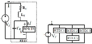
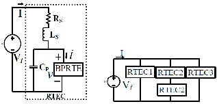
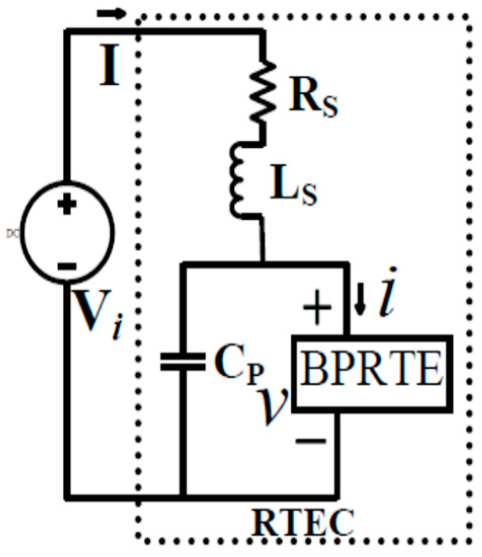
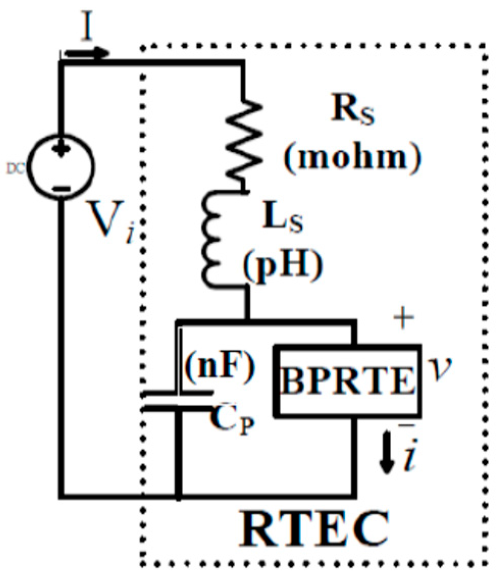
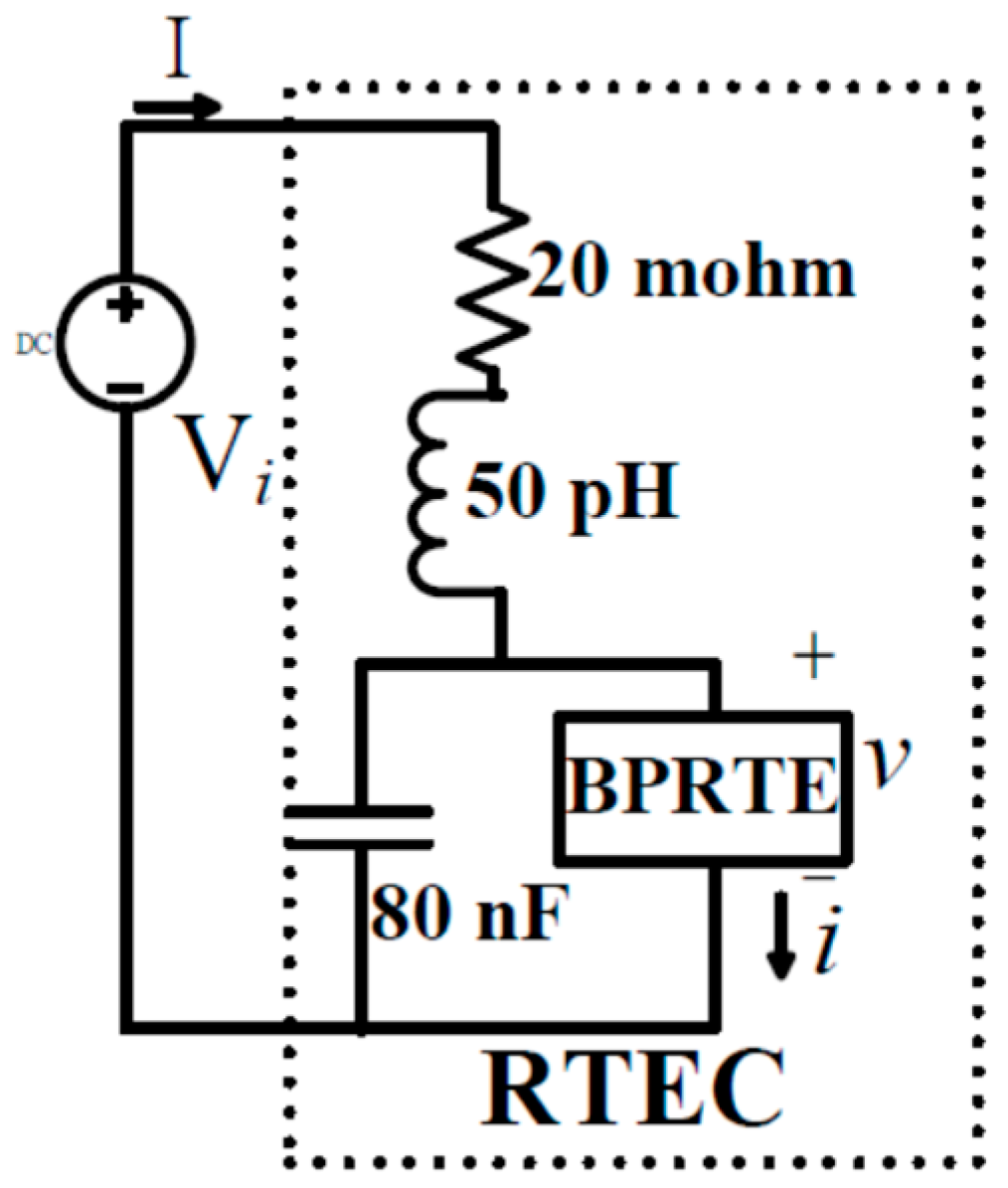
3.1. Design of RTEC Unit

In RTEC unit, its critical properties in current-voltage characteristic are including the peak current density (PCD) value (IP), peak voltage (PV) value (VP), peak-to-valley current ratio (PVCDR) value, threshold voltage (VT), negative differential resistance (NDR) value (RN), rising time (tr) of the RTEC current, and the operation oscillation frequency (fR). The critical properties are influenced by many key parameters including series resistance (RS), parallel capacitance (Cp), and lead inductance (LS) in RTEC unit. Therefore, the oscillation conditions of resonant tunneling in RTEC unit are also influenced by series resistance (RS), parallel capacitance (Cp), and lead inductance (LS) of RTEC unit. To enhance the capability of resonant tunneling in RTEC unit including PVCDR value and PCD value, the series resistance (RS), parallel capacitance (Cp), and lead inductance (LS) should be suitably evaluated. The more the peak-to-valley current density ratio (PVCDR) value is, the more the noise margin (Mn), the interference immunity capability (Cii), the logical swing (Sl), and the output power (Po) of RTEC unit are. The lower the threshold voltage (VT) value is, the less the output dissipated power of RTEC unit is. Low operation voltage will significantly decrease the peak voltage (VP) value of the RTEC unit in NDR property. As the parallel capacitance (Cp) value has been decreased, the operation oscillation frequency (fR) value will be increased and the rising time (tr) of the RTEC current will also be lowered. The decrease of series resistance (RS) value will enhance the operation oscillation frequency (fR) value of RTEC unit. Finally, as the lead inductance (LS) value of RTEC unit is decreased, the operation oscillation frequency (fR) value will be increased and the rising time (tr) of RTEC current will be also lowered as well. PVCDR value played an important role in the resonant tunneling properties of RTEC unit which can enhance the noise margin efficiency (Mn), improve the interference immunity capability (Cii), stabilize the logical swing (Sl) value, and increase the output power (Po) value. The correlations between the NDR characteristic of the RTEC unit and the resonant frequency, resonant conditions and resistivity frequency, so called operation oscillation frequency (fR) could be widely applied in electronic circuit designs of the transient circuit model and the dynamic unstable model [1].

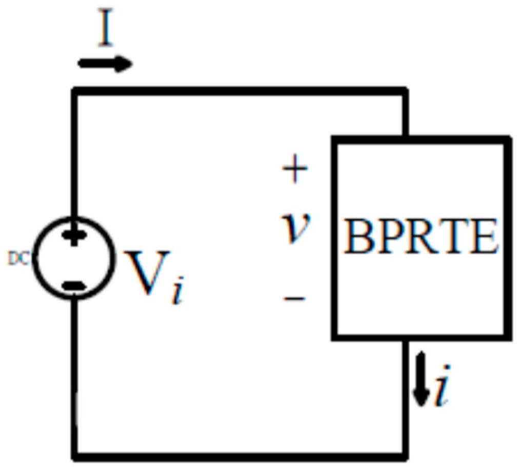
3.2. Simulation of Single PVCDR Value Using RTEC Unit without Cp, RS, and LS

The original BPRTE structure, as shown in Figure 2, is without external parasitic elements including Cp, RS, and LS which is expandable to compose the RTEC unit. The simulating result of the original BPRTE structure in I-V characteristics has been proposed in Ref. [1]. High PVCDR value and PCD value of BPRTE structure were, respectively exhibited reaching as 13.2 and 1.32 A in the NDR region [1].

3.3. Simulation of Single PVCDR Value Using RTEC Unit with Cp, RS, and LS

Participation of RS, Cp and LS in RTEC unit, so called external parasitic elements, will significantly influence the applications of RTEC unit in high frequency circuits and multiple value logical system. I-V characteristic of RTEC unit would be expectantly regulated, which resulted in the low PVCDR value and significant loading effect in RTEC unit for the initial selection of RS, Cp and LS. To construct the RTEC units with obvious double NDR regions and triple NDR regions, the optimum RS, Cp, and LS values in RTEC unit must be confirmed. After suitably selecting the Cp, RS, and LS values in simulation, as shown in Figure 3, the optimized PVCDR value in I-V characteristic was obtained. Firstly, the RS and LS of RTEC unit were fixed in the suitable values, and the Cp was controlled with five different values to find the optimum NDR characteristic. The NDR characteristic was optimized at the Cp value of 80 nF. Afterwards, as the external capacitance (Cp) and external inductance (LS) were also fixed in the suitable values, the external resistance (RS) was also explored by selected five different RS values to obtain the optimized NDR properties. As a result, the external resistance (RS) should be the resistance value of 20 mΩ which can obtain the optimized NDR characteristic. Finally, the external inductance (LS) value in the RTEC unit has been decided at the inductance value of 50 pH [1].
As shown in Figure 4, after the simulation of optimized NDR characteristic was finished, the optimum single PVCDR RTEC equivalent circuit with RS, Cp, and LS of 20 mΩ, 80 nF, and 50 pH respectively was constructed. The optimum single PVCDR NDR curve was characterized with PCD and PVCDR values of 1.35 A and 6.75 respectively. The external resistance (RS), external capacitance (Cp) and external inductance (LS) values in designs of double PVCDR RTEC and triple PVCDR RTEC structures were also decided using the same simulating method to obtain the optimum external PCD value and using the same calculation method to obtain the optimum PVCDR value.

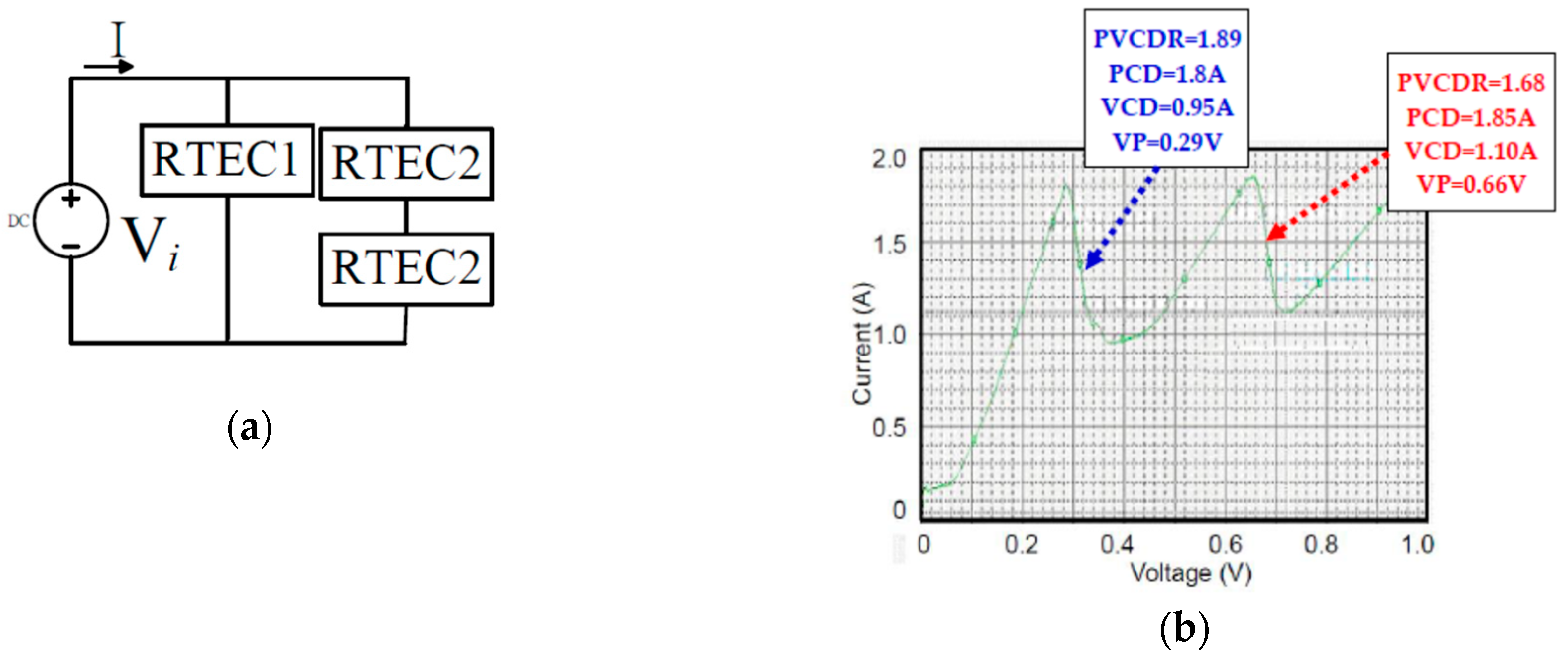
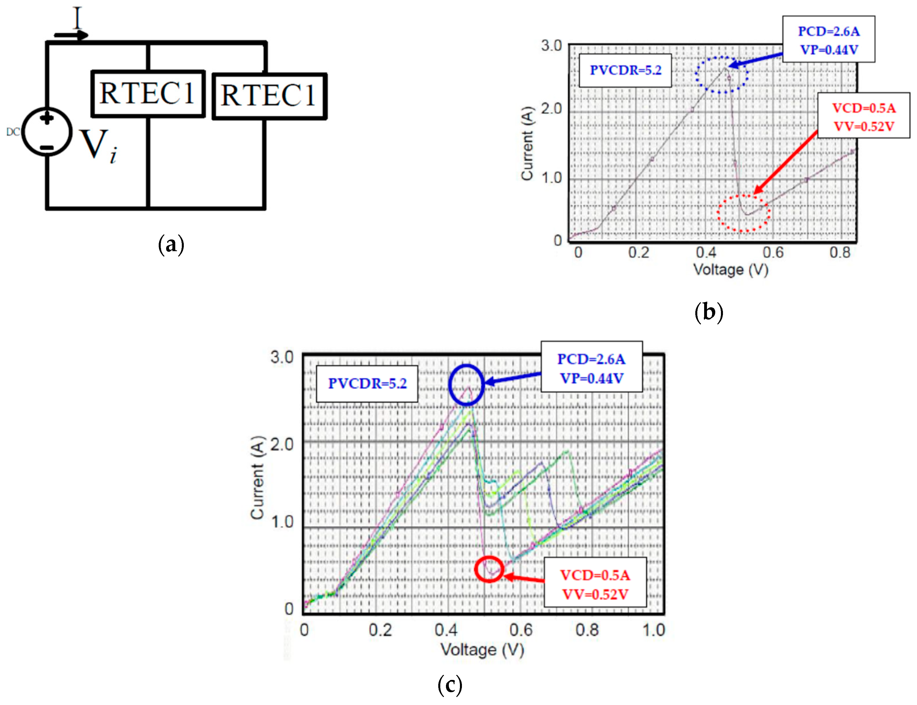
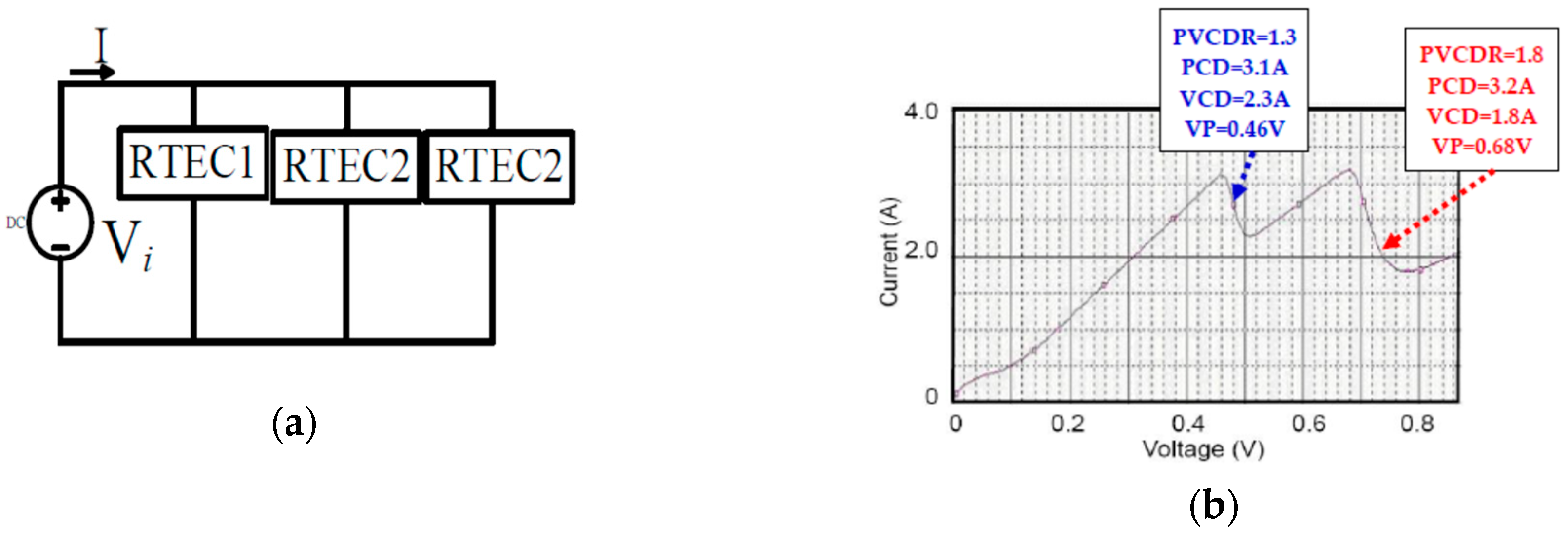
3.4. Simulation of Multiple PVCDR Values Using Two RTEC Units with Cp, RS, and LS

Two RTEC units, each is expressed as above, were in parallel to each other, as shown in Figure 5a. Cp, RS, and LS of paralleled RTEC units were all the same as those of the single PVCDR RTEC unit. In this simulation, the design of the double paralleled RTEC units obtained a PCD value as high as 2.6 A because of the decline of series resistances. The characteristic of double PVCDR values was not observed because of the unsuitable selection of RS value for the paralleled RTEC units, as shown in Figure 5b. When the RS of the first RTEC unit was large enough and the RS of the second RTEC unit was appropriately regulated, the characteristic of double PVCDR values will be clearly appeared, as shown in Figure 5c. In this research result, it revealed that although the RS has possessed the optimum values both in the first and in the second RTEC units, two PVCDR values and two PCD values in the double PVCDR RTEC were separately less than those in the single PVCDR RTEC, even though the double PVCDR phenomenon has been produced.
To enhance the NDR characteristic, another same single PVCDR RTEC unit was paralleled into a double PVCDR RTEC structure, as shown in Figure 6a. The PCD value of the improved PVCDR RTEC structure was significantly enlarged in the second NDR curve, and the PCD and VCD values of the first NDR curve were also simultaneously raised, which however resulted in the decrease of PVCDR values of both NDR curves. The different and asymmetrical PVCDR values of two NDR curves were ineffective in the application of an MVLL system because of the narrower logical level margin; its curve is indicated in Figure 6b.
Another method of improving double NDR curve was designed as shown in Figure 7a. The third RTEC unit was in series with one of two RTEC units in the double PVCDR RTEC unit, as exhibited in Figure 7a. In this configuration, the PVCDR values were heightened, as revealed in Figure 7b, in which the PVCDR values were respectively 1.89 and 1.68, and the PCD value reached about 1.80 A.

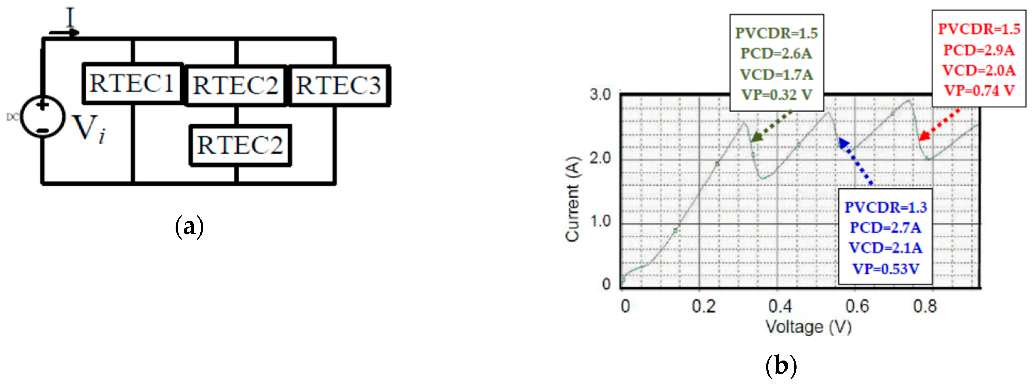
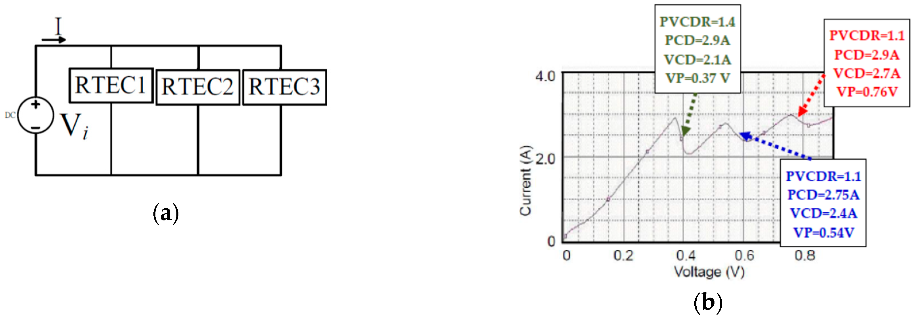
3.5. Simulation of Triple PVCDR Values Using RTEC Units with Cp, RS, and LS

Based on the good selection of three paralleled RTEC units, the three paralleled RTEC structure with triple PVCDR values was exhibited as shown in Figure 8a. The initial NDR research result of triple PVCDR RTEC structure as displayed in Figure 8b was not perfect in regard to the PVCDR values and PCD values in both symmetries and similarly for each NDR curves. To enable the significant of three NDR curves and to realize the similarity of three PVCDR values and PCD values, an improved triple PVCDR RTEC structure was proposed herein, as exhibited in Figure 9a, in which one of original PVCDR RTEC unit in triple PVCDR RTEC structure was arranged in series with the fourth PVCDR RTEC unit. Because of asymmetry of three PVCDR values, the triple PVCDR RTEC structure will not be properly applied in an MVLL system. The symmetry PVCDR values will be realized by adding the fourth PVCDR RTEC unit in series with the one of original PVCDR RTEC unit. The significant exhibition of symmetrical PVCDR values in a triple PVCDR RTEC structure design was due to the falling of valley current and adoption of suitable R1, R2 and R3 resistance elements, as revealed in Figure 9b. In order to avoid a floating state of circuit, a resistance R was connected to the fourth PVCDR RTEC unit.

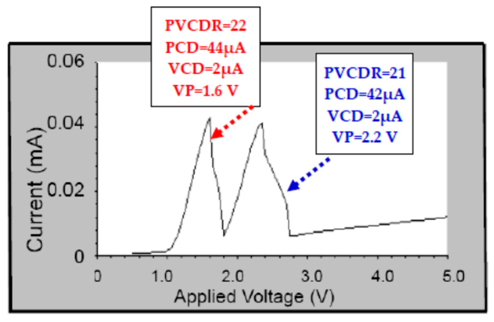
3.6. Experiment of Single PVCDR Value in RTEC Unit

The RTEC unit of Figure 2 was adopted for the experimental research to explore the NDR characteristic of the RTEC unit without external resistance (RS), external capacitance (Cp), and external inductance (LS). In the practical RTEC unit, the elements only include four resistors and two transistors. The resistors (R1, R2, R3, R4) were adopted to produce the different NDR characteristics under bias voltage in the designed RTEC units. The variety of bias voltage was to operate the “on” and “off” states of two transistors in the RTEC unit. “On” state or “off” state of the switching mode of two transistors in the RTEC unit formed a NDR-like curve. In this section, the practical circuit experiment of RTEC unit has been completed, including elements design, fabrication and measurements.
The practical circuit experiment of RTEC unit was implemented in this research, which included the elements design, fabrications and measurements. The explorations of VCD, PCD and PVCDR values from NDR curve played an important role to apply the RTEC unit in MVLL MD system. Low VCD value, high PCD value, and high PVCDR value were realized in the practical RTEC unit without parasitic effect. The BPRTE structure, so called RTEC unit without Cp, RS and LS values and including R1, R2, R3 and R4 of 16.6 kΩ, 10 kΩ, 0.7 kΩ, and 1 kΩ, respectively, constructed a single PVCDR RTEC structure, as shown in Figure 2. The bias voltage applied in a practical RTEC unit was 5 V. The experimental I-V characteristic for a single PVCDR RTEC structure was measured using a Keithley 2400 I-V instrument and data processing software. The PCD value and VCD value of the single PVCDR RTEC structure were about 32 μA and 1.4 μA, respectively, in this experiment. The PVCDR value of the single PVCDR RTEC structure in calculation was approximately 23. The PVCDR value of the single PVCDR RTEC structure was better than that of the RTPD structure in the semiconductor device. The cut-in voltage (Vr) and operation voltage were respectively about 0.5 V and 1.1 V [1]. Higher PVCDR in experiment than in simulation was attributed that the lower VCD value.
The low operation voltage would lower the power consumption and enable the RTEC unit which could be appropriately commercialized in 3C products. In experiment, the cut-in voltage (Vr) of the RTEC unit was reasonably less than 0.5 V. PCD value of about 32 μA in experiment was less than the PCD value of about 1.32 A in simulation [1]. Even though the parasitic and series resistances of practical RTEC unit in experiment were very striking, the NDR characteristics in experiment were similar with simulated results. PVCDR values in both experimental and simulating results were compared, in which the PVCDR value of a practical RTEC unit about 23 was more than the PVCDR value of the simulated RTEC unit of about 13.2 [1]. The high PVCDR value in experiment attributed to the lower VCD value in the practical RTEC unit.

3.7. Practical Double PVCDR RTEC Unit

A practical double PVCDR RTEC structure was constructed using two single PVCDR RTEC stages. R1, R2, R3, and R4 of 16.6 kΩ, 10 kΩ, 0.7 kΩ, and 1 kΩ were respectively adopted at the first stage of practical double PVCDR RTEC structure and also R1, R2, R3, and R4 of 32.8 kΩ, 10 kΩ, 1.1 kΩ, and 0.6 kΩ were respectively adopted at the second stage. The applied bias voltage in the practical RTEC unit was also 5 V. The experimental I-V characteristic of a double PVCDR RTEC structure was exhibited in Figure 10. In this experiment, two PCD values were about 0.044 mA and 0.042 mA respectively and two VCD values were almost the same, about 2 μA. The calculated two practical PVCDR values were approximately 22 and 21, respectively. The PCD values of practical RTEC unit, about 0.044 mA and 0.042 mA, were still less than the simulating results, about 1.80 A and 1.85A, but were similar to the experimental value in practical single PVCDR RTEC structure. Higher PCD value and higher VCD value for the practical double PVCDR RTEC structure compared to those of practical single PVCDR RTEC structure were attributed to the less output load effect from previous stage, which however resulted in the low PVCDR value in a practical double PVCDR RTEC structure.

4. Conclusions

PVCDR RTEC structures using BPRTE element without parasitic passive elements exhibited a single NDR characteristic were researched both in simulation and in experiment respectively. However, the PVCDR RTEC structures using BPRTE element with parasitic passive elements exhibited a single NDR characteristic were also explored in simulations. The simulation results of PV and VV values considering the external parasitic effects were similar with the experimental results than without considering the external parasitic effects. However, the simulation results of PCD, VCD, and PVCDR values without considering the external parasitic effects were more close to the experimental results than with considering the external parasitic effects. The results of simulating research and experimental research were compared with each other, as shown in Table 1.

Funding

This research received no external funding.

Conflicts of Interest

The author declares no conflict of interest.

References

  1. Yang, C.C. Influence of parasitic effects in negative differential resistance characteristics of resonant. In Proceedings of the IEEE International Symposium on Computer, Consumer and Control, Taichung, Taiwan, 6–8 December 2018. [Google Scholar]
  2. Ji, Y.C.; Chang, S.; Wang, H.; Huang, Q.; He, J.; Yi, F. Multi-valued logic design methodology with double negative differential resistance transistors. IET Micro Nano Lett. 2017, 12, 738–743. [Google Scholar] [CrossRef]
  3. Yang, C.C. High performance multiple stepped quantum well resonant microwave devices. Electron. Lett. 2006, 42, 1485–1487. [Google Scholar] [CrossRef]
  4. Yang, C.C.; Su, Y.K. Well-defined electrical properties high-strain resonant interband tunneling structure. Microelectron. J. 2008, 39, 67–69. [Google Scholar] [CrossRef]
  5. Yang, C.C.; Su, Y.K. High performance aluminum arsenic intraband resonant microwave devices. Microelectron. J. 2008, 39, 90–93. [Google Scholar] [CrossRef]
  6. Tsu, R.; Esaki, L. Tunneling in a finite superlattice. Appl. Phys. Lett. 1973, 22, 562–564. [Google Scholar] [CrossRef]
  7. Mokhov, A.; Burns, F.P.; Murphy, J.P.; Koelmans, A.; Yakovlev, A. Mixed radixreed-muller expansions. IEEE Comput. 2012, 61, 1189–1202. [Google Scholar]
  8. Khan, M.E.; Lee, J.H.; Byeon, S.J.; Kim, Y.H. Semimetallicity and negative differential resistance from hybrid halideperovskite nanowires. Adv. Funct. Mater. 2019, 29, 1807620. [Google Scholar] [CrossRef]
  9. Felix, A.B.; Pacheco, M.; Orellana, P.; Latgé, A. Negative differential resistance in hybrid carbon-based structures. Phys. Rev. 2019, B99, 195442. [Google Scholar] [CrossRef]
  10. Seabaugh, A.C.; Kao, Y.C.; Yuan, H.T. Nine-state resonant tunneling diode memory. IEEE Electron. Device Lett. 1992, 13, 479–481. [Google Scholar] [CrossRef]
  11. Zhou, J.R.; Han, G.Q.; Li, J.; Liu, Y.; Peng, Y.; Zhang, J.C.; Sun, Q.Q.; Zhang, D.W.; Hao, Y. Negative differential resistance in negative capacitance EFTs. IEEE Electron. Device Lett. 2018, 39, 622–625. [Google Scholar] [CrossRef]
  12. Atmaca, Ö.; Narin, P.; Kutlu, E.; Malin, T.V.; Mansurov, V.G.; Zhuravlev, K.S.; Lişesivdin, S.B.; Özbay, E. Negative differential resistance observation and a new fitting model for electron drift velocity in GaN-based heterostructures. IEEE Trans. Electron. Devices 2018, 65, 950–956. [Google Scholar] [CrossRef]
  13. Ulansky, V.; Raza, A.; Oun, H. Electronic circuit with controllable negative differential resistance and its applications. Electronics 2019, 8, 409. [Google Scholar] [CrossRef]
  14. Shin, J.M.; Ko, E.N.; Shin, C.H. Analysis on the operation of negative differential resistance Fin FET with Pb (Zr0.52Ti0.48)O3 threshold selector. IEEE Trans. Electron. Devices 2018, 65, 19–22. [Google Scholar] [CrossRef]
  15. Hwang, W.S.; Tahy, K.; Myers-Ward, R.L.; Campbell, P.M.; Eddy, C.R., Jr.; Gaskill, D.K.; Xing, H.; Seabaugh, A.C.; Jena, D. Fabrication of top-gated epitaxial grapheme nano-ribbon FETs using hydrogen silsesquioxane (HSQ). J. Vac. Sci. Technol. B 2012, 30, 104–108. [Google Scholar] [CrossRef]
  16. Zhang, T.; Guérin, D.; Alibart, F.; Vuillaume, D.; Lmimouni, K.; Lenfant, S.; Yassin, A.; Oçafrain, M.; Blanchard, P.; Roncali, J. Functions based on monolayer devices derived from gold nanoparticles functionalized with electropolymerizable TEDOT units. J. Phys. Chem. C 2017, 121, 10131–10139. [Google Scholar] [CrossRef]
  17. Breuil, L.; Haspeslagh, L.; Blomme, P.; Wellekens, D.; DeVos, J.; Lorenzini, M.; Van Houdt, J. A new scalable self-aligned dual-bit split-gate charge-trapping memory device. IEEE Trans. Electron. Devices 2005, 52, 2250–2257. [Google Scholar] [CrossRef]
Figure 1. Scheme of basic resonant tunneling electronic circuit (RTEC) unit [1].
Electronics 08 00673 g001
Figure 2. Single PVCDR RTEC unit without Cp, RS, and LS [1].
Electronics 08 00673 g002
Figure 3. Single PVCDR RTEC unit with Cp, RS and LS values [1].
Electronics 08 00673 g003
Figure 4. Optimum single PVCDR RTEC equivalent circuit with Cp of 80 nF, RS of 20 mΩ and LS of 50 pH values [1].
Electronics 08 00673 g004
Figure 5. (a) Paralleled structure of two PVCDR RTEC units. (b) Single NDR curve of paralleled structure of two PVCDR RTEC units with PCD value of 2.6 A. (c) Double NDR curve of double PVCDR RTEC structure with variable RS.
Electronics 08 00673 g005
Figure 6. (a) Improvement of double PVCDR RTEC structure by paralleled the third RTEC unit. (b) Improvement of NDR characteristic with different and asymmetry PVCDR values after paralleled another same single PVCDR RTEC unit.
Electronics 08 00673 g006
Figure 7. (a) The second improvement method by the double PVCDR RTEC structure in series with another RTEC unit. (b) Improvement of NDR characteristic by the method of the double PVCDR RTEC structure in series with another RTEC unit.
Electronics 08 00673 g007
Figure 8. (a) The construction of triple PVCDR RTEC structure. (b) NDR curve of triple PVCDR RTEC structure.
Electronics 08 00673 g008
Figure 9. (a) The equivalent circuit of triple PVCDR RTEC structure with adding the fourth RTEC unit. (b) Symmetry NDR characteristic of triple PVCDR RTEC structure with adding the fourth RTEC unit.
Electronics 08 00673 g009
Figure 10. I-V curve of practical double PVCDR RTEC structure.
Electronics 08 00673 g010
Table 1. Comparisons of PVCDR RTEC structures.
Characteristics of Single PVCDR RETC
PCD (A)VCD (A)PV (V)VV (V)PVCDR
nth NDR peak1st1st1st1st1st
Simulation without Cp, RS, LS [1]1.320.100.250.4413.2
Simulation with Cp, RS, LS [1]1.350.200.280.466.75
Experiment without Cp, RS, LS [1]32μ1.4μ1.11.223
Paralleled structure of units2.60.50.440.525.2
Ref [13]15m6m1.757.02.5
Characteristics of Double PVCDR RTEC
PCD (A)VCD (A)PV (V)VV (V)PVCDR
nth NDR peak1st1st1st1st1st
Simulation with Cp, RS, LS1.800.950.290.361.89
Experiment without Cp, RS, LS44μ2 μ1.601.8022
Characteristics of Double PVCDR RTEC
PCD (A)VCD (A)PV (V)VV (V)PVCDR
nth NDR peak2nd2nd2nd2nd2nd
Simulation with Cp, RS, LS1.851.100.660.721.68
Experiment without Cp, RS, LS42μ2.202.8021
Characteristics of Triple PVCDR RETC
PCD (A)VCD (A)PV (V)VV (V)PVCDR
nth NDR peak1st1st1st1st1st
Simulation with Cp, RS, LS2.61.70.320.361.5
Experiment without Cp, RS, LS36μ24μ1.21.31.5
Characteristics of Triple PVCDR RETC
PCD (A)VCD (A)PV (V)VV (V)PVCDR
nth NDR peak2nd2nd2nd2nd2nd
Simulation with Cp, RS, LS2.72.10.530.531.3
Experiment without Cp, RS, LS44μ1.61.85.5
Characteristics of Triple PVCDR RETC
PCD (A)VCD (A)PV (V)VV (V)PVCDR
nth NDR peak3rd3rd3rd3rd3rd
Simulation with Cp, RS, LS2.92.00.740.771.5
Experiment without Cp, RS, LS46μ10μ2.22.84.6

