Article

Optimization of a Series Converter for Low-Frequency Ripple Cancellation of an LED Driver

1
LEMUR Group, Department of Electrical Engineering, University of Oviedo, 33204 Gijon, Spain
2
ce3i2 Group, Department of Electrical Engineering, University of Oviedo, 33204 Gijon, Spain
3
GEDRE Group, Universidade Federal de Santa Maria, Santa Maria, RS 97010, Brazil
4
GSEC Group, Universidade Federal de Santa Maria, Santa Maria, RS 97010, Brazil
*
Author to whom correspondence should be addressed.
Electronics 2019, 8(6), 664; https://doi.org/10.3390/electronics8060664
Submission received: 8 May 2019 / Revised: 31 May 2019 / Accepted: 10 June 2019 / Published: 12 June 2019
(This article belongs to the Special Issue Latest Developments in LED Drivers)

Abstract

:
In this paper, the optimization of the power and control stages of a previously proposed topology for an off-line LED electronic driver is presented. The full system avoids the use of electrolytic capacitors at the D C link, therefore increasing the lifespan and reliability of the driver. As a consequence of having a relatively small capacitance, the D C link operates with a large Low-Frequency ( L F ) voltage ripple. This work presents a design optimization for the power and control stages of a current-fed bidirectional buck converter, operating as the LED current control stage. As this block processes only the A C power arising from the L F voltage ripple, it can increase the system efficiency against the typical two-stage solution. In the original proposal, the main drawback was the high inductor losses due to the resulting large inductor currents and large inductance value. The proposed optimization ensures an enhanced design of the inductor while keeping a constant current through the LEDs. A new optimization methodology is proposed and the theoretical results have been validated in a built prototype for a 40 W LED lamp.

1. Introduction

Presently, LED lighting systems are gaining more importance as they provide a tool for a more rational use of electrical energy on household, public lighting systems, transportation, commercial applications, etc. [1,2]. Therefore, one of the major power electronic development fields is related to the enhancement of efficient high-performance electronic lighting systems for LED lamps. The main features to consider when designing an LED driver are its D C voltage source behavior (a D C driving stage able to limit the LED current must be used), the long operating life (the driver must last at least as long as the LED itself), and the color variations (there are some parameters that affect the color such as the waveforms, the operating temperature, etc.).
For low requirement applications, simple, passive, or cost-effective solutions can be used to deal with the D C behavior of the LED lamp [3]. For instance, [4] presents a linear regulator integrated with an LED lamp that provides an optimal solution in terms of power density for single LED applications. But generally speaking, linear regulators are not recommended when the application requires a high number of LEDs (as the overall efficiency of the system turns more critical) or when high-performance control schemes are needed. In fact, the driver might also include additional features such as dimming—either Amplitude Modulated ( A M ) dimming or Pulse Width Modulation ( P W M ) dimming—, current derating, etc. Linear regulators can be used for implementing A M dimming, but in case P W M dimming is required (to avoid color shift or stability problems at low power, as in higher power LED Lamps), switch-mode regulators are much more adequate. Also, the future deployment of D C grids will allow significant simplification in the LED driver topologies used for D C applications [5]. However, taking into account the regulations and standards that lighting equipment must fulfill, in most cases high-performance drivers are required. The LED driving system must provide not only A C - D C efficient conversion, but also LED current control, Power Factor Correction ( P F C ) and input current Total Harmonic Distortion ( T H D ) control.
As the lifespan of the driver is expected to match that of the LED lamp [6], some constraints are derived for the design of the electronic stage [7]. For instance, large electrolytic capacitors usage is highly inadvisable, considering their shorter operating life compared to the life of the LED lamp [8]. Many recent works in the literature agree that large capacitance values for the power stage of LED drivers need to be avoided [9,10,11,12,13,14,15]. In order to achieve this goal, electrolytic capacitors must be discarded. Therefore, researchers have come up with novel control strategies [16,17,18,19] as well as optimized topologies [6,13,20,21,22,23,24,25,26,27,28,29,30,31,32,33] that imply smaller capacitances in the D C link, to overcome this issue.
Two-stage schemes are the most common approach when designing single-phase LED ballasts. A first active P F C stage controls the power factor and the line current harmonics content. Considering a power factor close to unity, the input power to this active stage pulsates at twice the line frequency. In order to guarantee the instant power balance, this input stage delivers the pulsating power to a second stage, interfaced through an energy storage device. This storage part is usually a capacitive device at the D C link. The main voltage ripple component at this capacitor, at twice the line frequency, is a function of the capacitance value, taking into account that higher capacitances mean smaller ripple amplitudes. To ensure proper operation of the system, and to effectively control the output power through the LEDs—and hence the emitted light—standard output stages require a low voltage ripple at the D C link. This guarantees a given constant D C current through the LEDs. These large capacitance values are implemented by means of electrolytic technology devices, which achieve such high capacitance values in reasonable component size.
In the conventional scheme, each of the stages processes the full amount of power, ensuring enough design flexibility as it decouples the input and the output constraints, allowing for simple solutions. However, this usually results in relatively low efficiencies, higher volume, and components count.
A second strategy divides the output power of the input stage in two different power flows. The largest share of this power is delivered directly to the LED lamp, while the rest of the power (including the A C part) is processed by a second stage. This ensures the A C power ripple cancellation at the load [29,30,31,32]. Upon careful design considerations, this scheme provides an overall system efficiency increase, as most of the power is processed only once.
The approach followed in this work delivers all the D C part of the output power of the input stage, and uses a second stage to process only the A C . Therefore, this bidirectional stage stores energy in some intervals and sends it back to the D C link in others. Provided that adequate management of the A C power is carried out, the resulting power through the LEDs will be pure D C , therefore allowing for higher ripples and smaller capacitances at the D C link. This capacitance reduction is the main purpose of the proposed topological scheme. Given that these low capacitance values can be achieved with technologies such as plastic film capacitors, thus avoiding the reliability problems derived from the use of electrolytic parts, therefore extending the lifespan of the system. In particular, this work improves the performance of the system presented in [33] but including a deeper analysis that allows for an optimal design strategy in terms of power density and efficiency.
The design of the second stage has one degree of freedom, which is related to the inductance value of an inductive energy storage device, L S t o . Therefore, the performance of the output stage (size, weight, power losses, dynamic behavior, etc.) largely depends on this L S t o value. In a first approach, the design of this inductor is carried out by analyzing the steady state, open loop operation of the circuit, for different L S t o inductance values, considering two key dimensions of this performance. These two factors are losses on one hand (both copper and core losses), and size (and therefore weight) on the other hand. A trade-off between those two dimensions is initially achieved, although it is considered to be unfeasible, as it will be justified. After that, a novel closed-loop operation analysis of the output stage has been carried out, and as it will be shown, a smaller, yet more efficient design of the inductor L S t o will be achieved, considering the same trade-off approach in terms of losses vs. size than in the steady-state analysis previously discussed. This work shows the detailed procedure of the optimization process, and demonstrates its feasibility through simulations and by experimental validation on a 40 W design example.
The paper is divided as follows. Section 2 deals with the considered LED driving strategy. Later, Section 3 presents and discusses the proposed topology and its basic operation. Section 4 and Section 5 show the switching and dynamic equations of the open loop operation respectively, in order to obtain the transfer functions of the proposed scheme. A design example for open loop operation is given in Section 6, while Section 7 shows the simulation results obtained with this configuration. The control scheme implemented for closed-loop operation is discussed in Section 8, whereas Section 9 shows the experimental results of the closed-loop operation of the converter. Finally, Section 10 shows the main conclusions of this work as well as the future developments.

2. Bidirectional Output Stage for LED Drivers

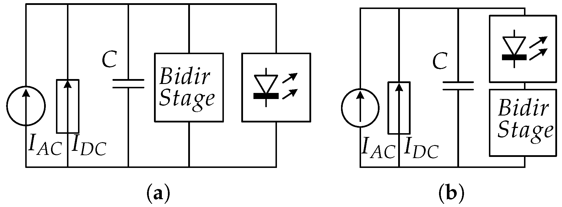
To process the A C power at the D C link, two possibilities can be used, based on the connection of the stage and the LED lamp. Figure 1 depicts both cases, and as it can be seen, the equivalent circuit of the input PFC stage is modeled by a D C current source, I D C , in parallel with an A C current source, I A C , charging the D C link capacitor, C.
Figure 1a shows the parallel configuration that uses an additional capacitor as main storage device [13,32]. This work uses the series configuration proposed in [33] and depicted in Figure 1b. From this diagram, it can be understood that the voltage ratings in this stage are smaller than the D C link ratings, allowing for the use of low voltage components. Also, the proposed converter must allow single polarity current flow, but it must enable voltage blocking capability with both positive and negative polarities. Although it is out of the scope of this work, it must be commented that the series scheme has inherent P W M dimming capability, just by turning on and off the series stage. In terms of efficiency, the switches are rated for relatively low voltage values, which implies smaller parasitic elements in general terms, which provide expected benefits in switching and conduction losses. However, as it will be seen throughout the work, the most important concern is related to the losses at the storage inductor. This work presents a new design methodology for the control scheme of the bidirectional stage, targeting the optimization of this inductor. Thus, the full system efficiency is increased when compared to the previous design proposed in [33].

3. Proposed Topology

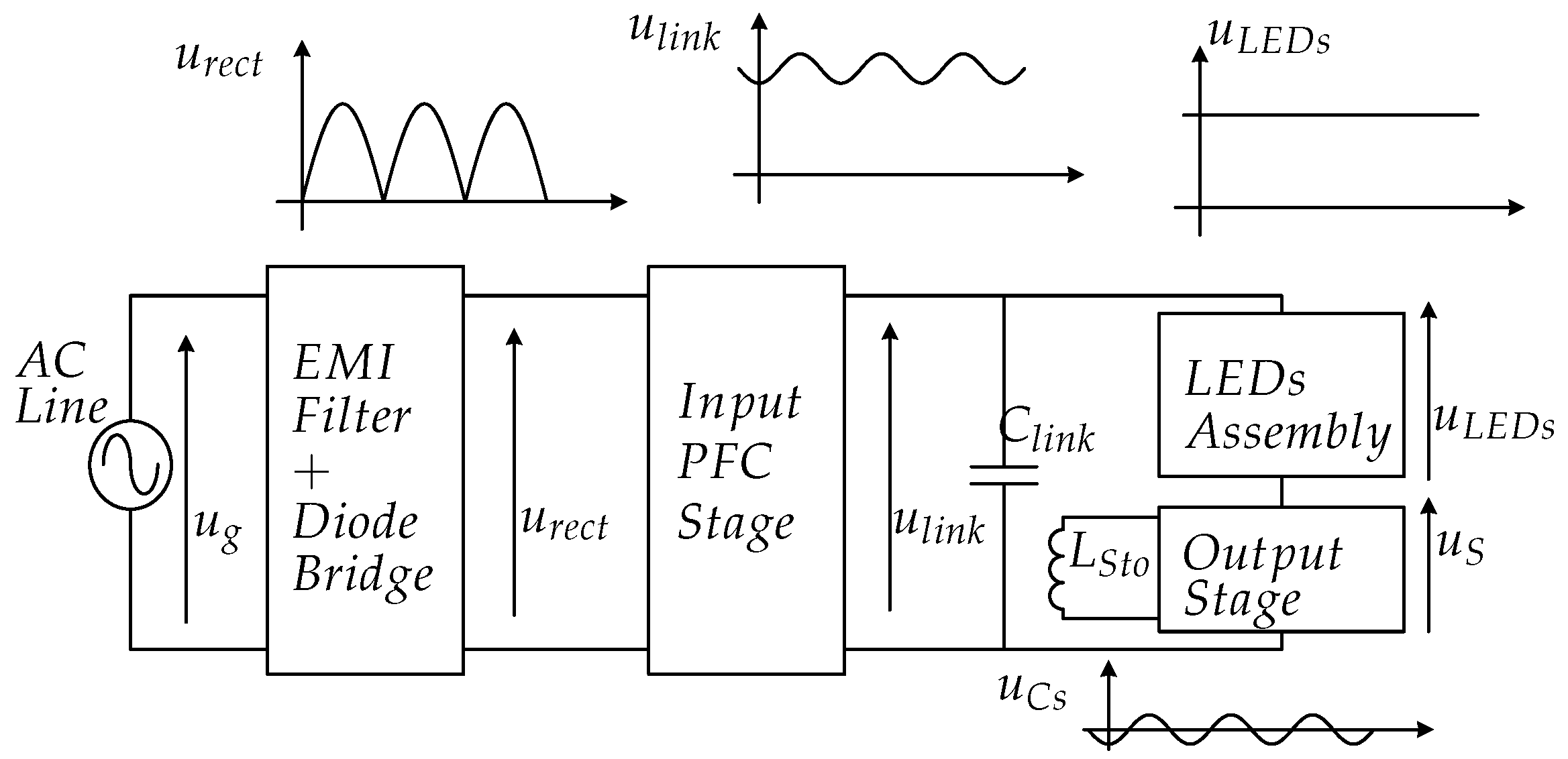
Figure 2 shows the block diagram of the full off-line High Frequency ( H F ) LED driver with the followed approach. After being rectified and filtered, the input voltage enters the input P F C stage, which processes the energy towards the D C link capacitor, C l i n k . However, the selection and proper design of this input stage is out of the scope of this work. The input of the second stage, u C s , is connected in series with the LEDs assembly. As a small capacitance value is selected for the capacitor C l i n k , in order to avoid electrolytic technologies, a significant A C L F ripple appears at the D C link voltage, u l i n k . Figure 2 also depicts the simplified waveforms in the expected operation of the system (pure D C voltage at u L E D s , and pure A C voltage at u C s as well).
Figure 3a details the topology of the system. A grid-side PFC stage is implemented by means of a Discontinuous Conduction Mode ( D C M ) buck-boost converter, in order to provide unity power factor with constant duty ratio. This input stage supplies power from the grid towards the D C link. Connected to this DC link, the proposed bidirectional series circuit can be seen. This stage is a current-fed bidirectional buck converter, formed by switches Q A and Q B , capacitor C S and the storage inductor, L S t o . The input of this stage is considered to be the LEDs current, i L E D s , with the output variable being the current through the inductor L S t o , i S t o . Q A and Q B have been represented as bipolar transistors for simplicity, as they must be able to block reverse voltages. In the final prototype, they will be implemented by means of MOSFET transistors with a series blocking diode. Figure 3b depicts again the main L F voltage waveforms at the driver, sharing the time axis.

4. HF Analysis of the Proposed Topology

The H F and L F analysis of the basic topology for this application has already been presented in [33]. The most important conclusions to this analysis are reviewed in this work. The H F analysis employs a fixed frequency control, denoting the switching period as T. The common H F analysis in power electronics is based on considering that the system operates in steady state. Therefore, the significant waveforms of the most relevant devices can be calculated for one switching period, keeping in mind that for any magnitude considered to be a function of time, x ( t ) , the following equation is fulfilled:
x ( t ) = x ( t + T )
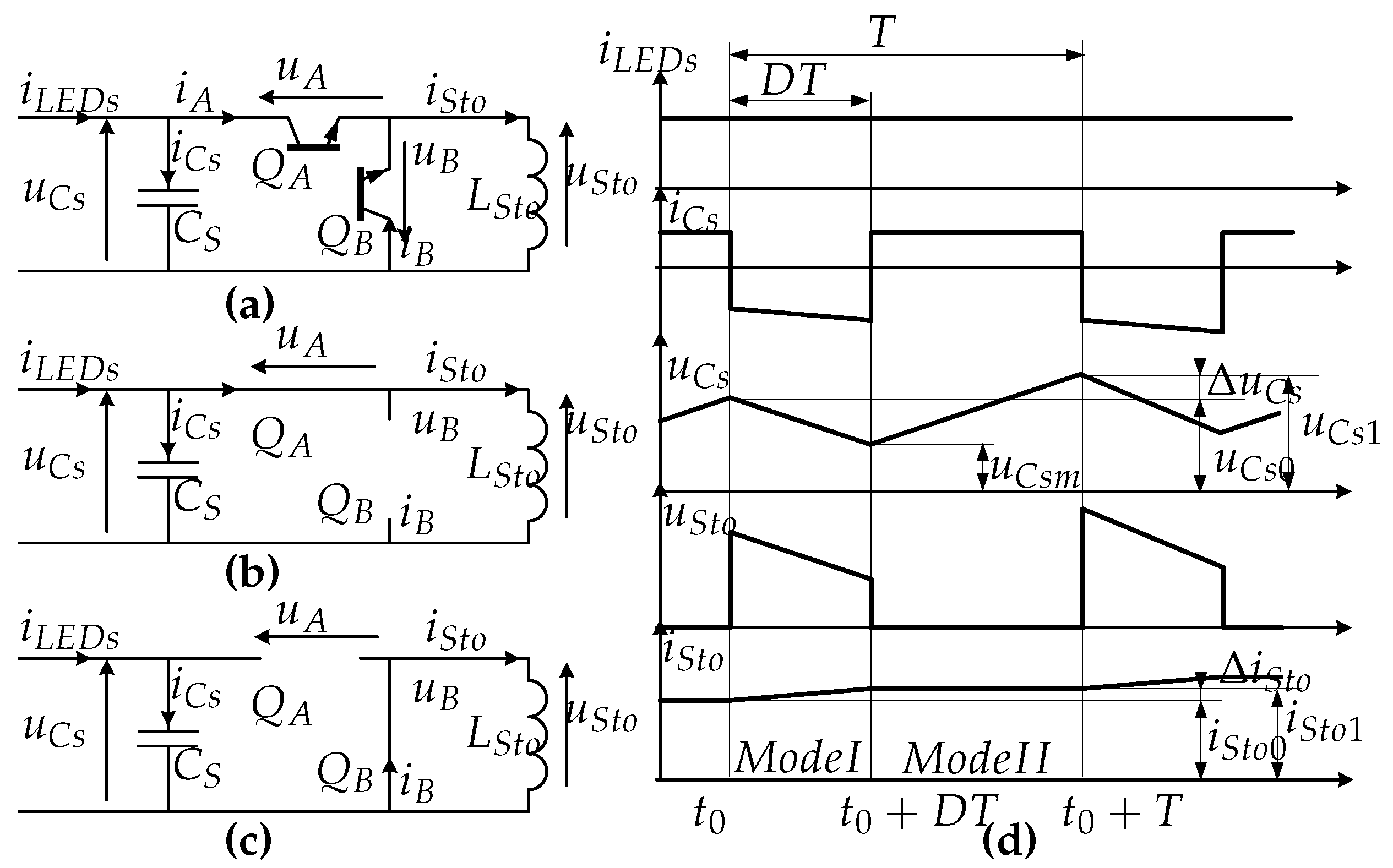
This is achieved through a power balance, as the circuit input power in one period equals the power delivered to the output stage. It must be taken into account that there is not an output load in the proposed stage able to dissipate active power. This implies that the input power in one switching period will not be dissipated. In turn, the energy will be stored within the storage inductor, L S t o , by changing the electric parameters at this device. Therefore, the analysis cannot be based on considering steady state in a switching period, and (1) is not fulfilled anymore. Instead, this analysis must be focused on finding the variations of the capacitor voltage, u C s ( t ) , and the storage inductor current, i S t o ( t ) , in a switching period, while the LEDs current remains constant. Figure 4a shows the voltage and current references considered during the analysis. Only complementary operation of switches Q A and Q B is considered. The duty ratio, D, is defined for switch Q A . Given that the current through the storage inductor will flow either through Q A or Q B , thus:
i A ( t ) | T < i S t o ( t ) | T
where i A ( t ) is the forward current through Q A (see Figure 4a, and the expression x ( t ) | T denotes the average value of a generic magnitude x ( t ) in a switching period, T. Furthermore, (2) ultimately states that the current flowing through the storage inductor will always be greater than the LEDs current. The H F analysis considers two switching modes in a switching period. While Q A is turned on and Q B is turned off, i.e., 0 < t < D · T , the system operates in Mode I. On the other hand, for the complementary state of the switches, i.e., D · T < t < T , the converter operates in Mode II. The full analysis of these modes is given in [33], and only the main statements are summarized here. At instant t 0 , the values of the storage inductor current and the input capacitor are, respectively:
i S t o ( t 0 ) = i S t o 0
u C s ( t 0 ) = u C s 0
After a switching period T, the waveforms are expressed by:
i S t o ( t 0 + T ) = i S t o 0 + Δ i S t o
u C s ( t 0 + T ) = u C s 0 + Δ u C s
After some calculations [33], the final expressions for these parameters can be expressed as:
u C s ( t 0 + T ) = u C s 0 + i L E D s C S · ( 1 D ) · T
Δ u C s = i L E D s C S · T i S t o 0 C S · D T Δ i S t o 2 · C S · D T
Δ i S t o = u C s 0 L S t o · D T + 1 2 u C s L S t o · D T
Finally, from (8) and (9):
Δ u S = i L E D s i S t o · D u C s 0 2 L S t o C S + D 2 T 2 4 L S t o · T
Δ i S t o = u C s 0 · D L S t o 1 D 2 T 2 4 L 2 C S + D 2 T 2 4 L S t o + D T i L E D s i S t o 0 · D 2 L S t o C S + D 2 T 2 4 L S t o T
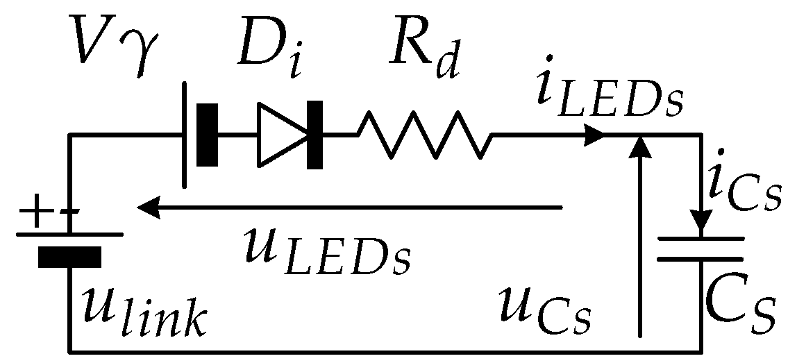
The expression of the H F current ripple through the LEDs can be calculated considering Mode II. In this interval, the capacitor current, i C s , equals the current through the LEDs. Considering that the D C link behaves as a voltage source at H F , then the resulting circuit for this subinterval can be seen in Figure 5, in which the LEDs assembly is modeled by a series connection of an ideal diode D i , a dynamic resistor R d , and a threshold voltage V γ . Therefore the A C ripple of the current through the LEDs can be calculated considering an exponential discharge through the dynamic resistance of the LEDs, R d :
Δ i L E D s = Δ u C s R d

5. Dynamic Analysis of the Proposed Topology

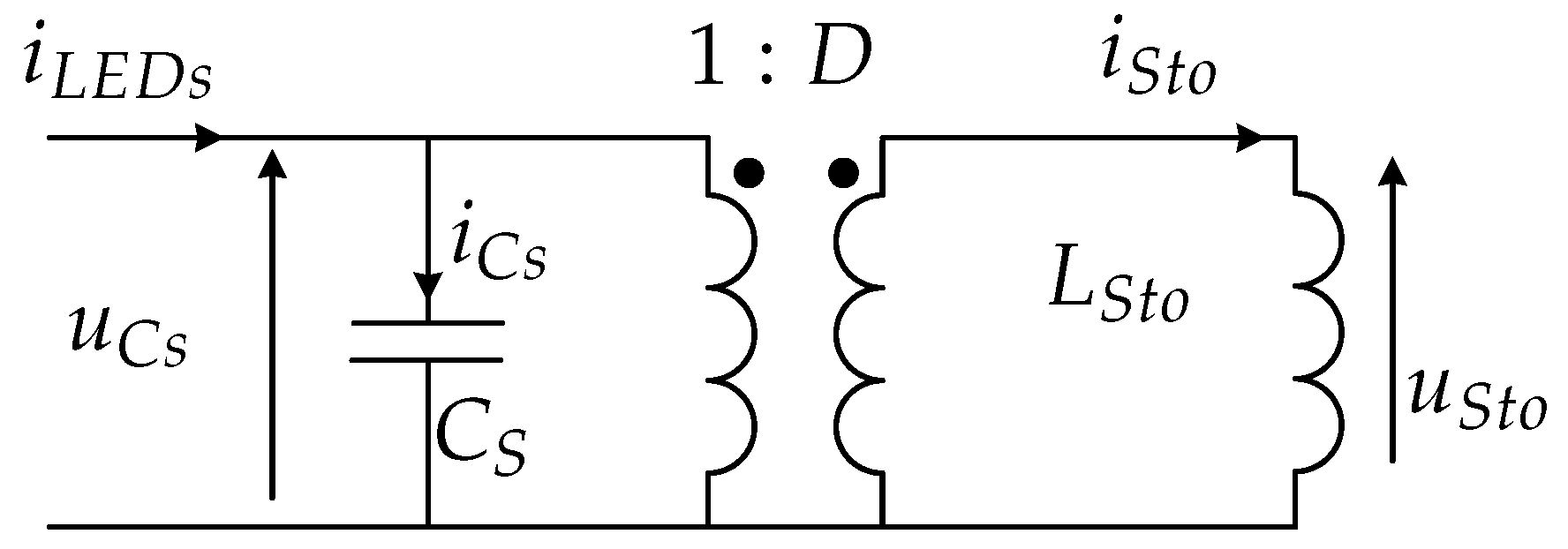
The study of the L F average model of the main circuit magnitudes enables the dynamic analysis of the system, which in turn is required for designing the control system. Considering (10), (11), and the waveforms in Figure 4d, the following expressions are found for the capacitor and the inductor waveforms, respectively:
C S · d u C s ( t ) d t | L F = i L E D s ( t ) i S t o ( t ) · D
L S t o · d i S t o ( t ) d t | L F = D · u C s ( t )
These equations yield the L F equivalent circuit in Figure 6, for the second stage of the LED driver. The ideal transformer takes into account the effect of the switching of Q A and Q B with a duty ratio D for Q A .

6. Design Example for a 40 W LEDs Assembly

With the previous analysis, a design example is proposed for a XLamp® XR-E LED (part XREWHT-L1-0000-00D01) from Cree®, in a series connection assembly of 36 devices, accounting for a nominal power of 40 W. the design parameters of the input PFC stage can be seen in Table 1. The input values for the design are shown in Table 2. In order to design the power stage, both values of L S t o and C S must be calculated. A target value for the LEDs current ripple will be 10%, considering this parameter is equally split into a 5% at H F and a 5% at L F .
The value of the H F voltage ripple at capacitor C S is given by the capacitor charge when Q A is turned off:
Δ v C h a r g e = 1 C S · ( 1 D ) · i L E D s · T
Therefore, the H F current ripple through the LEDs will be:
Δ i L E D s = Δ v C h a r g e R d
The worst case will be when D 0 . Therefore, from (15), (16) and Table 2, for a 5% H F ripple in the output current, the H F current ripple through the LEDs will be:
C S i L E D s · T R d · Δ i L E D s = 5.6 μ F
The value of the storage inductor, L S t o , can be calculated considering the performance of the system. The first approach, taken into account in [33], is to supply the system in open loop, with a constant duty ratio, in this case D = 0.1 , and check the evolution of the waveforms. Upon these conditions, the inductor is chosen as follows. From Figure 6, for a constant duty ratio, and after referring the inductance value to the primary side of the equivalent transformer, the expression for the current through the LEDs becomes:
i ^ L E D s = u ^ L E D s · 1 + s 2 · C S · L S t o D 2 s · L S t o D 2
This yields an expression of L S t o given by:
L S t o = Δ u C s · D 2 2 · π · f R I P P L E ( Δ i L E D s + Δ u C s · 2 · p i · f R I P P L E · C S )
Therefore, the value of L S t o depends on the selected fixed duty ratio, D. The design solution must be optimized in terms of size (core volume of the inductor) and efficiency (losses in the switches and in the inductor). A series of preliminary data has been calculated for four different duty ratio parameters. These figures are represented in Table 3:
From Table 3, it can be seen how the larger the duty ratio, the larger the inductance, allowing for larger core sizes. However, this would imply smaller currents through the inductor, which in turn implies smaller losses. On the other hand, smaller duty ratios cause higher effects of non-linear aspects (switching times, etc.) and parasitic elements. In order to take a final decision, an optimal design of the inductor has been carried out for each of these duty ratio values. This design provides the sizes of the cores, the A C and D C losses in the inductors, the number of turns, air gap, etc. For simplicity, the core geometry has been restricted to the commercial E T D shape; however, the full series of size has been considered (from E T D 29 to E T D 59 ). These results are presented in Table 4, Table 5, Table 6 and Table 7, for E T D cores, of 3 F 3 magnetic material. The proximity effect has been included within the losses while the skin effect skin-depth which limits the diameter in case it is too large.
As an initial guess, a 10% duty ratio has been selected as the minimum value allowing proper operation of the converter. Assuming the total losses in the inductor of around 10% of the output power levels, then from (19) and Table 3:
L S t o = 3 mH
D = 0.1
I L S t o = 3.5 A
For this inductance choice, Table 5 shows the different coil designs that minimize losses for each ETD size considered. Aiming to balance the size and the losses, the ETD44 size has been selected, and it is represented in bold characters.

7. Validation of the Open Loop Approach

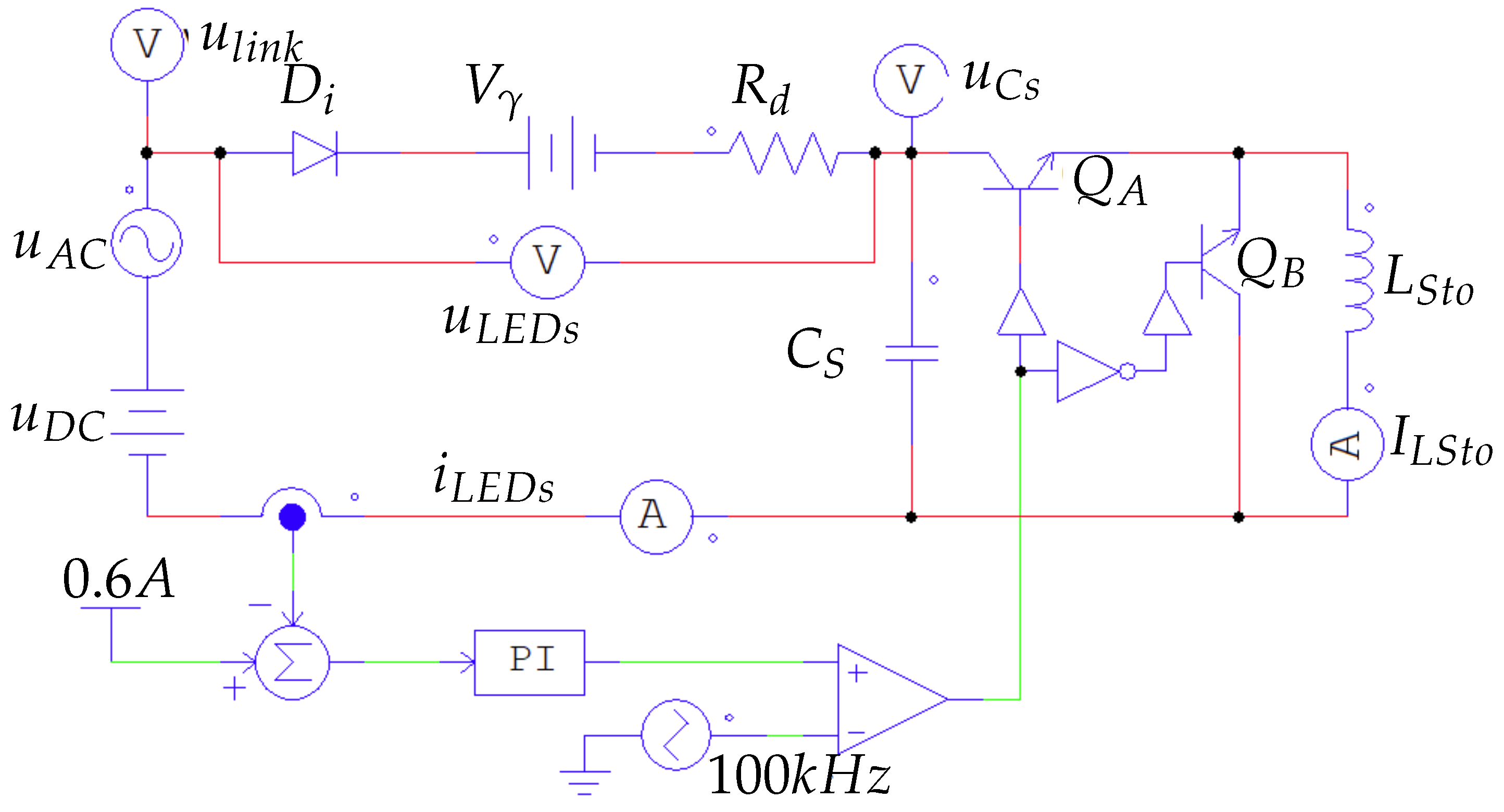
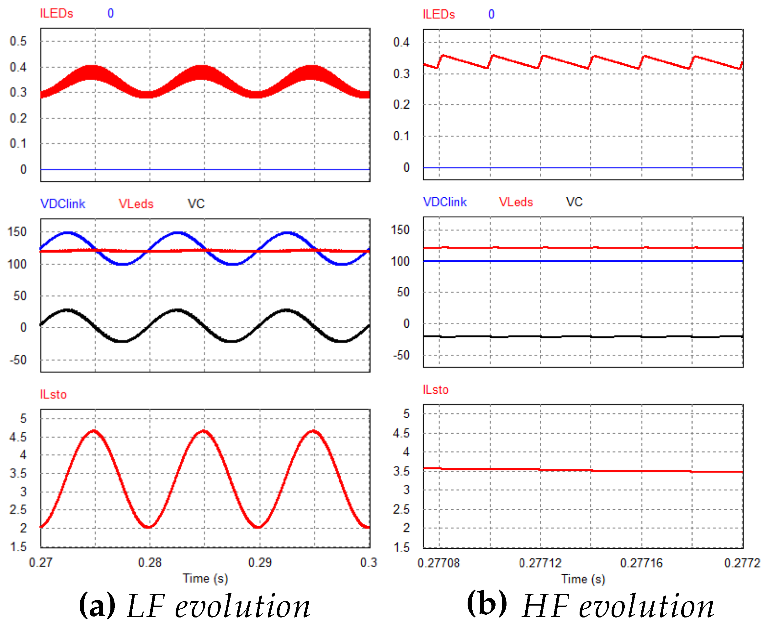
To validate this approach, a simulation has been carried out with the system parameters stated above. The simulation simplified schematics file for P S I M can be seen in Figure 7. However, the simulation results shown in Figure 8 take also into account the parasitic components of the elements in Figure 7.
In Figure 8a, the L F evolutions of D C link voltage, the capacitor C S voltage, and the LEDs voltage are shown. As it can be seen, all the A C voltage of the D C link is held by C S , and thus the LEDs voltage is a D C voltage. The resulting LEDs current can also be seen, still presenting a 100 Hz ripple, although for requirement applications it could be considered acceptable, as some directives allow relatively high HF harmonics levels [34]. Figure 8b shows the H F switching system waveforms at 50 kHz, again at full power level. Even though the design provides good results in terms of ripple cancellation and efficiency, the overall size ( E T D 44 for a 40 W converter) results too high, implying an unfeasible solution. In order to achieve a smaller core size, an analysis of the closed-loop control of the system will be carried out, and, as it will be demonstrated, results in a smaller inductor value for the same L F current ripple cancellation levels.

8. Closed-Loop Control of the Proposed Topology

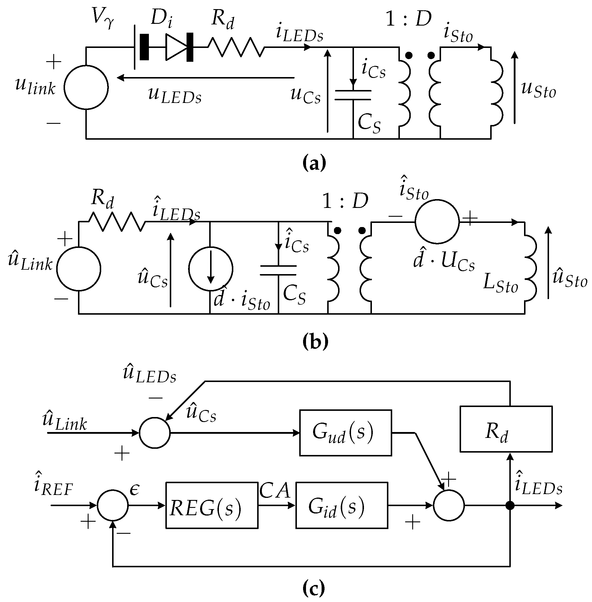
Figure 9a depicts the equivalent L F model of the second stage including the LEDs assembly. The u l i n k voltage source models the output voltage behavior of the input P F C stage, including both the D C and the L F A C ripple voltage components at the D C link capacitor. As in the previous discussion, the equivalent circuit that models the LEDs assembly is formed by an ideal diode, D i , in series with a D C source, V γ , and a resistor, R d . V γ and R d account for the total threshold voltage and the total dynamic resistor of the LEDs setup, respectively. After following a small-signal analysis approach (linearize and perturb) [33], the final small-signal A C model of the circuit is shown in Figure 9b. After some calculations, the transfer functions of the system are finally given by:
G i d ( s ) = i ^ L E D s ( s ) d ^ ( s ) = U C s D · R d · s · I S t o · L S t o U C s · D + 1 s 2 · L S t o · C S D 2 + s · L S t o D 2 · R d + 1
G i u ( s ) = i ^ L E D s ( s ) u C s ^ ( s ) = 1 R d · s 2 · L S t o · C S D 2 + 1 s 2 · L S t o · C S D 2 + s · L S t o D 2 · R d + 1
where G i d is the transfer function representing the duty ratio, d ^ , to the LEDs current, i ^ L E D s , and G i u is the transfer function representing the voltage across the capacitor, u ^ S , also to i ^ L E D s . Capital letters represent steady-state parameters, while lower case letters with the symbol ^ represent small-signal variables.
Figure 9c shows the system block diagram that depicts the current control scheme implemented in the LEDs driver. The current error, ϵ , is the input of the regulator block, R E G ( s ) . The output of this block is the control action, C A , that corresponds to the duty ratio of switch Q A . From (23), it can be seen that the open loop transfer function is a second order system. A PI controller, with a bandwidth of 1 kHz and a phase margin of 45° has been tuned using S I S O T o o l of M A T L A B , resulting in the following parameters:
R E G ( s ) = K p · 1 + 1 s · T I = 8.1 · 10 12 · 1 + 1 s · 2.9 · 10 5
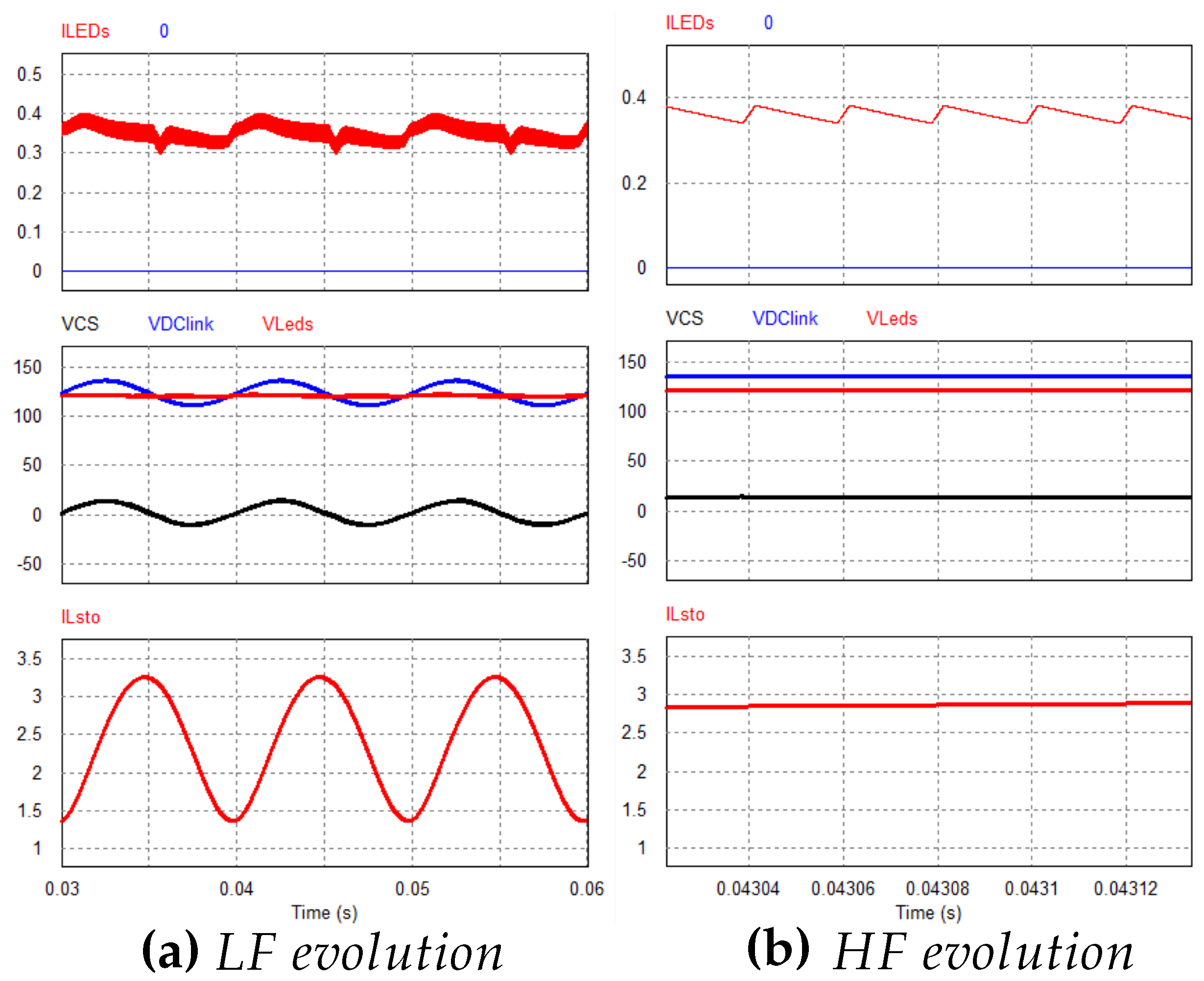
Figure 10 depicts some simulation waveforms of the closed-loop system with such a controller. As it can be seen, the L F ripple results in a much smaller value than the obtained in open loop. Nevertheless, given that the perturbation represented by the D C link voltage ripple, u ^ l i n k , is continuously changing at twice the grid reference, a complete error cancellation is not possible with a PI regulator. In fact, this error, G L F C R ( s ) , can be calculated as:
G L F C R ( s ) = i ^ L E D s ( s ) u ^ L i n k ( s ) | i ^ L E D s = G i u ( s ) 1 + R E G ( s ) · G i d ( s ) + R d · G i u ( s )
The value of this error is a function of the storage inductor, L S t o , and of the parameters of the regulator. This opens an interesting option, which is to optimize the design (including the inductance value and the regulator parameters) for a given target parameter. In this case, the target will be to decrease the inductance value, keeping constant the control parameters (bandwidth and phase margin), and ensuring that the L F ripple is equal or smaller than in the open loop case. Table 8 shows a set of designs for different inductor values, along with the resulting control parameters that ensure relatively similar dynamic performance.
To make a decision, the design solution must be optimized in terms of size (core volume of the inductor), efficiency (losses in the switches and in the inductor) and implementation (allowing enough control margins in the control action variable). For very small L S t o values, the control action gets too high, and the control loop is unable to operate properly in the carried-out simulations. On the other hand, very high values of L S t o yield large size cores, which result in non-practical design values. Thus, the optimal solution has been chosen as L S t o = 300 µH (highlighted in bold characters in Table 8). For this new value of the inductor, a new design is given in Table 9. Again, and in order to balance the size and the losses in the core, the ETD34 size has now been selected, and it is represented in bold characters in Table 9.
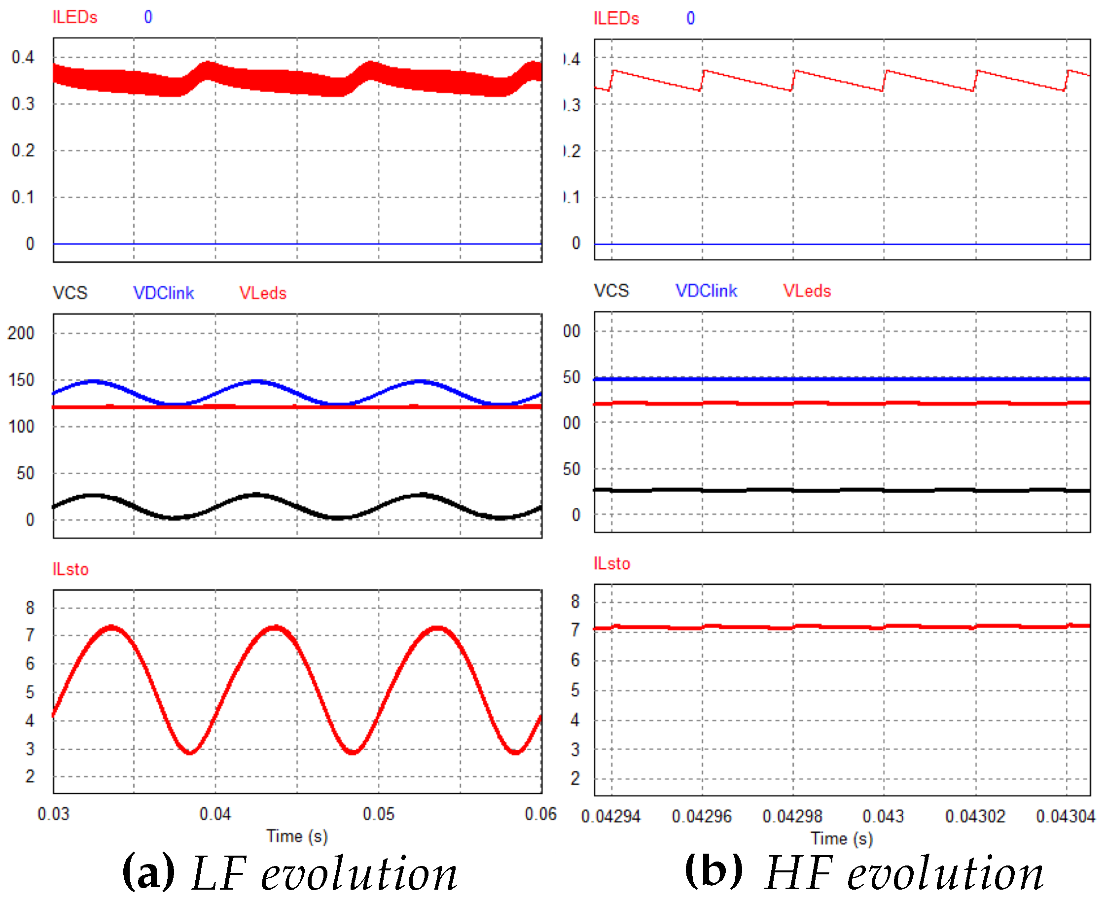
Comparing Table 5 and Table 9, a theoretical 2 W power losses decrease in the total inductor losses can be achieved, accounting for around a 5% efficiency gain. This is obtained even moving to an E T D 34 core size, significantly smaller than the first guess, and much more adequate for a 40 W design. The system has been again simulated for the PI controller selected from Table 8. Figure 11 shows the simulated behavior of the system. As it can be seen, the resulting LEDs current ripple has also a smaller value, therefore the design has been optimized in terms of inductor size. However, as the real inductor is much smaller, the inductor average current and LF current ripple is larger. As the system needs to avoid the current to evolve to negative values (as switches Q A and Q B cannot withstand negative currents), the capacitor C S voltage presents a D C offset. This ensures low ripple in the LEDs current, but unfortunately provides a decrease in the system efficiency. These losses are represented, for the inductor values considered, in the last row of Table 8.
Therefore, with the new inductor, there is an increase of 4.3 W in the system power losses due the capacitance offset required for proper operation of the output stage. However, from Table 5 and Table 9, a saving of 2.1 W is obtained in the inductor L S t o (as its inductance decreases by a factor of ten). Therefore, considering the power balance, the global loss increase is around 2.2 W for this solution, but significantly decreasing the size of the inductor (from E T D 44 to E T D 34 ). Depending on the particular application considered, a trade-off must be carried out, in order to select the optimal size of the inductor.

9. Experimental Results of the Closed-Loop Operation

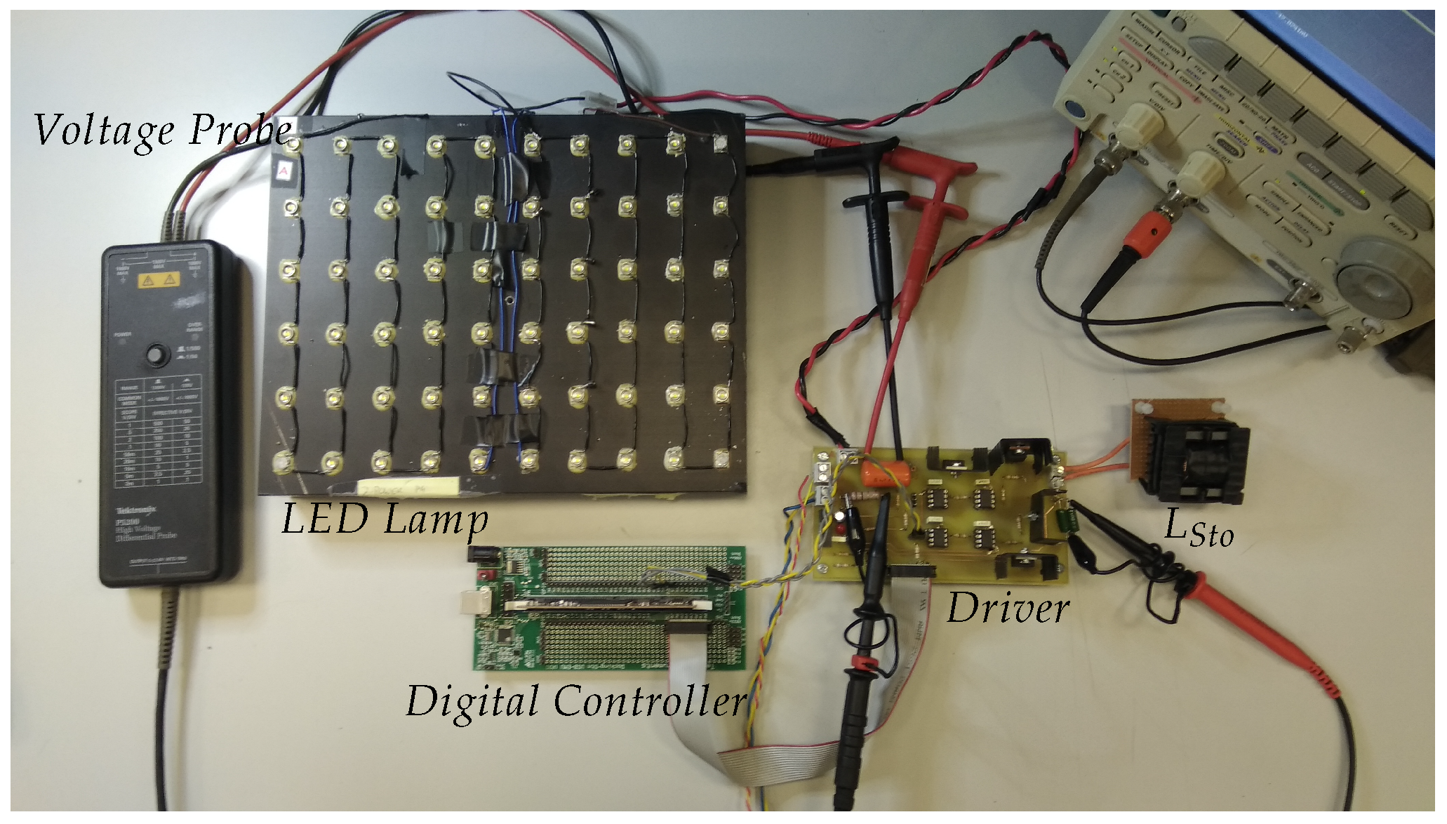
To validate the design, a prototype of the proposed second stage has been built and tested. This prototype is shown in Figure 12, along with the LED Lamp and the digital controller.
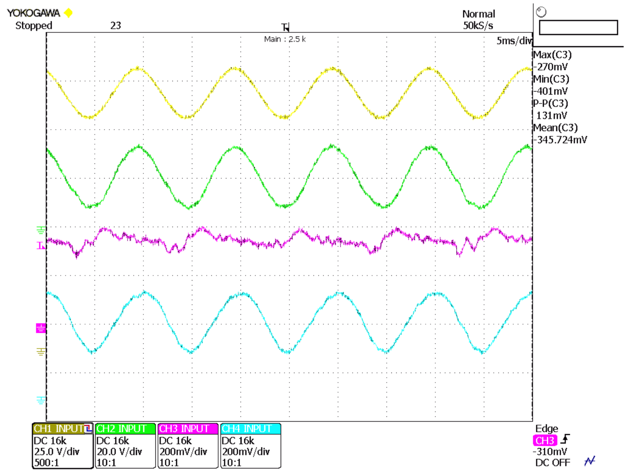
The built LED driver is intended for a lamp with the specifications given in Section 6 and Table 2. The system is operating with the optimal inductor from Table 9 (i.e., E T D 34 , L = 300 µH), for a steady-state operation at a nominal current of 350 mA. The P I controller of the current loop has the parameters defined in Table 8 for this inductance value. The input of the setup is a programmable D C voltage source H P 6812 A , in order to control the average and ripple values of the D C link voltage. The switches have been implemented connecting in series a B Y W 29200 G diode from O n S e m i and an I R F 640 from I R . Figure 13 shows the steady-state operation of the system. As it can be seen, the steady-state operation is similar to the one depicted in the simulations at Figure 11.
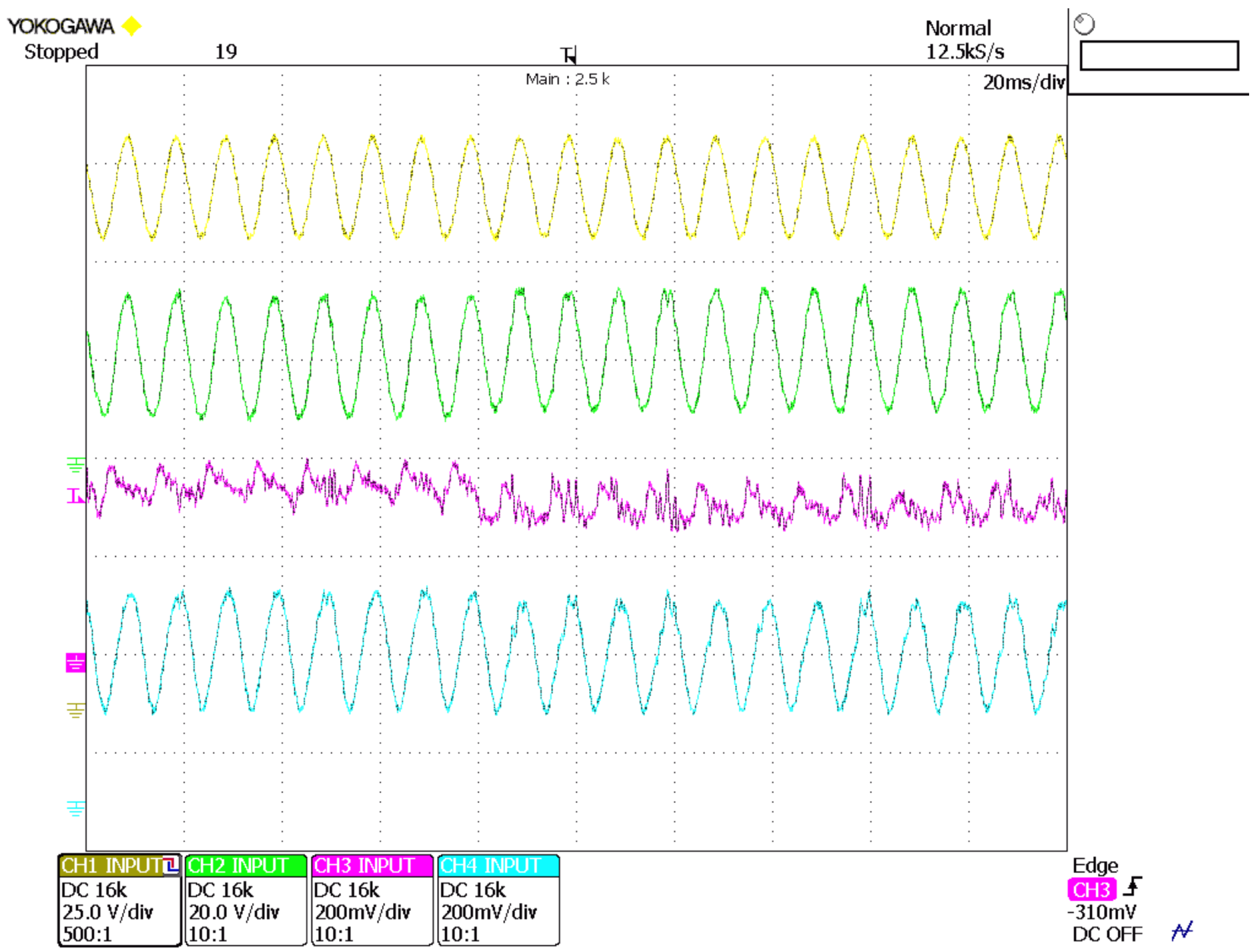
The final power losses at the output stage are 6.4 W, allowing for a final efficiency of this secondary stage of 87%. It can be noted how in this particular design, the primary goal is the size reduction of the converter; higher efficiencies can be achieved at the cost of increasing the core size. Figure 14 finally shows the dynamic performance of the controller, upon a current step from 350 mA to 300 mA. As it can be seen, the system reaches the new steady state in less than half a line frequency cycle.

10. Conclusions and Future Developments

The LED driver topology proposed in [33] for the output stage of an electronic driver for power LEDs has been deeply analyzed, and a new design methodology for optimizing the converter size has been proposed. This methodology has been validated both by simulations and experimentally. The advantages of this improved methodology are mainly two: first, the optimization of the inductor design which implies that the resulting inductor value can be built in an E T D 34 core, and secondly, the dynamics of the controller are improved allowing for comparably faster performance which implies that the proposed series scheme is suitable for L F P W M dimming control.
The main drawbacks of the proposed driver are the number of components (two extra switches, which in addition must be driven with isolated drivers, as well as the reactive elements C S and L S t o ), plus the mandatory current control loop (including sensor, microcontroller, etc.). Comparing the closed-loop control schemes, in standard LED drivers, the D C link voltage control is mandatory, while the LED current control can be achieved without a dedicated closed loop (for instance, in open loop by means of a peak current control through the LEDs); however, with the proposed series output stage, the LED current control is also necessary to attain proper operation of the stage. Future developments of the work include the design of a full off-line driver, also considering the input P F C stage in the control system, as well as the experimental validation of the system operating under P W M dimming scheme. Also, alternative control methods such as peak current control or resonant current control can be explored.
Author Contributions

Conceptualization, J.G. and M.A.D.C.; Supervision, J.G. and M.A.D.C.; Validation, J.G., S.S., P.Q., J.C., R.G., M.A.D.C. and D.C.; Writing—original draft, J.G.; Writing—review & editing, S.S., P.Q., J.C., R.G., M.A.D.C. and D.C.

Funding

This work has been partially supported by the Innovation Development and Research Office (MEC), Spanish Government, under Research Grants ENE2013-44245-R, Project “Microholo” and ENE2016-77919, Project “Conciliator”, and by the European Union through ERFD Structural Funds (FEDER); This work has been partially supported by the Government of the Principality of Asturias, Grant No. FC-GRUPIN-IDI/2018/000241, and under “Severo Ochoa” program of predoctoral grants for training in research and university teaching, grant number BP16-133; This work has been partially supported by INCT-GD, CNPq proc 465640/2014-1, CAPES proc 23038.000776/2017-54, and FAPERGS proc 17/2551-0000517-1.

Conflicts of Interest

The authors declare no conflict of interest. The founding sponsors had no role in the design of the study; in the collection, analyses, or interpretation of data; in the writing of the manuscript, or in the decision to publish the results.

Abbreviations

The following abbreviations are used in this manuscript:
MDPIMultidisciplinary Digital Publishing Institute
DOAJDirectory of open access journals
TLAThree letter acronym
LDlinear dichroism

References

  1. Shur, M.S.; Zukauskas, R. Solid-State Lighting: Toward Superior Illumination. Proc. IEEE 2005, 93, 1691–1703. [Google Scholar] [CrossRef]
  2. Weir, B. Driving the 21st century’s lights. IEEE Spectr. 2012, 49, 42–47. [Google Scholar] [CrossRef]
  3. Chen, W.; Li, S.N.; Hui, S.Y.R. A comparative study on the circuit topologies for offline passive light-emitting diode (LED) drivers with long lifetime amp; high efficiency. In Proceedings of the 2010 IEEE Energy Conversion Congress and Exposition, Atlanta, GA, USA, 12–16 September 2010. [Google Scholar] [CrossRef]
  4. Soh, M.Y.; Teo, T.H.; Selvaraj, S.L.; Peng, L.; Disney, D.; Yeo, K.S. Heterogeneous Integration of GaN and BCD Technologies. Energies 2019, 8, 351. [Google Scholar] [CrossRef]
  5. Alonso, J.M.; Perdigão, M.S.; Dalla Costa, M.A.; Martínez, G.; Osorio, R. Analysis and Experiments on a Single-Inductor Half-Bridge LED Driver With Magnetic Control. IEEE Trans. Power Electron. 2017, 32, 9179–9190. [Google Scholar] [CrossRef]
  6. Almeida, P.S.; Camponogara, D.; Dalla Costa, M.; Braga, H.; Alonso, J.M. Matching LED and Driver Life Spans: A Review of Different Techniques. IEEE Ind. Electron. Mag. 2015, 9, 36–47. [Google Scholar] [CrossRef]
  7. Narendran, N.; Gu, Y. Life of LED-based white light sources. J. Disp. Technol. 2005, 1, 167–171. [Google Scholar] [CrossRef]
  8. Stevens, J.L.; Shaffer, J.S.; Vandenham, J.T. The service life of large aluminum electrolytic capacitors: Effects of construction and application. IEEE Trans. Ind. Appl. 2002, 38, 1441–1446. [Google Scholar] [CrossRef]
  9. Arias, M.; Lamar, D.G.; Sebastian, J.; Balocco, D.; Diallo, A.A. High-Efficiency LED Driver Without Electrolytic Capacitor for Street Lighting. IEEE Trans. Ind. Appl. 2013, 49, 127–137. [Google Scholar] [CrossRef]
  10. Nassary, M.; Orabi, M.; Arias, M.; Ahmed, E.M.; Hasaneen, E.S. Analysis and Control of Electrolytic Capacitor-Less LED Driver Based on Harmonic Injection Technique. Energies 2018, 11, 3030. [Google Scholar] [CrossRef]
  11. Gu, L.; Ruan, X.; Xu, M.; Yao, K. Means of Eliminating Electrolytic Capacitor in AC/DC Power Supplies for LED Lightings. IEEE Trans. Power Electron. 2009, 24, 1399–1408. [Google Scholar] [CrossRef]
  12. Ma, H.; Lai, J.; Feng, Q.; Yu, W.; Zheng, C.; Zhao, Z. A Novel Valley-Fill SEPIC-Derived Power Supply Without Electrolytic Capacitor for LED Lighting Application. IEEE Trans. Power Electron. 2012, 27, 3057–3071. [Google Scholar] [CrossRef]
  13. Qiu, Y.; Wang, L.; Wang, H.; Liu, Y.; Sen, C.P. Bipolar Ripple Cancellation Method to Achieve Single-Stage Electrolytic-Capacitor-Less High-Power LED Driver. IEEE J. Emerg. Sel. Top. Power Electron. 2015, 3, 698–713. [Google Scholar] [CrossRef]
  14. Cosetin, M.R.; Bitencourt, E.A.; Bolzan, T.E.; da Silva, M.F.; Alonso, J.M.; do Prado, R.N. Comparison of integrated SEPIC-Buck and SEPIC-Ćuk converters as off-line dimmable LED drivers with reduced storage capacitor. In Proceedings of the 2014 16th European Conference on Power Electronics and Applications, Lappeenranta, Finland, 26–28 August 2014; pp. 1–10. [Google Scholar] [CrossRef]
  15. Pereira, G.G.; Dalla Costa, M.A.; Alonso, J.M.; De Melo, M.F.; Barriquello, C.H. LED Driver Based on Input Current Shaper Without Electrolytic Capacitor. IEEE Trans. Ind. Electron. 2017, 64, 4520–4529. [Google Scholar] [CrossRef]
  16. Gacio, D.; Alonso, J.M.; Garcia, J.; Campa, L.; Crespo, M.J.; Rico-Secades, M. PWM Series Dimming for Slow-Dynamics HPF LED Drivers: The High-Frequency Approach. IEEE Trans. Ind. Electron. 2012, 59, 1717–1727. [Google Scholar] [CrossRef]
  17. Dyble, M.; Narendran, N.; Bierman, A.; Klein, T. Impact of dimming white LEDs: Chromaticity shifts due to different dimming methods. In Proceedings of the Fifth International Conference on Solid State Lighting, San Diego, CA, USA, 31 July–4 August 2005. [Google Scholar] [CrossRef]
  18. White, B.; Wang, H.; Liu, Y.; Liu, X. An Average Current Modulation Method for Single-Stage LED Drivers with High Power Factor and Zero Low-Frequency Current Ripple. IEEE J. Emerg. Sel. Top. Power Electron. 2015, 3, 714–731. [Google Scholar] [CrossRef]
  19. Poorali, B.; Adib, E.; Farzanehfard, H. A Single-Stage Single-Switch Soft-Switching Power-Factor-Correction LED Driver. IEEE Trans. Power Electron. 2017, 32, 7932–7940. [Google Scholar] [CrossRef]
  20. Cheng, C.; Yen, C. A single-stage driver for high power LEDs. In Proceedings of the 2011 6th IEEE Conference on Industrial Electronics and Applications, Beijing, China, 21–23 June 2011; pp. 2666–2671. [Google Scholar] [CrossRef]
  21. Bęczkowski, S.; Munk-Nielsen, S. Two phase interleaved buck converter for driving high power LEDs. In Proceedings of the 2011 14th European Conference on Power Electronics and Applications, Birmingham, UK, 30 August–1 Semtember 2011; pp. 1–6. [Google Scholar]
  22. Gobbato, C.; Kohler, S.V.; de Souza, I.H.; Denardin, G.W.; Lopes, d.P.J. Integrated Topology of DC–DC Converter for LED Street Lighting System Based on Modular Drivers. IEEE Trans. Ind. Appl. 2018, 54, 3881–3889. [Google Scholar] [CrossRef]
  23. Arias, M.; Castro, I.; Lamar, D.G.; Vázquez, A.; Sebastián, J. Optimized Design of a High Input-Voltage-Ripple-Rejection Converter for LED Lighting. IEEE Trans. Power Electron. 2018, 33, 5192–5205. [Google Scholar] [CrossRef]
  24. Cardesin, J.; Ribas, J.; Garcia-Garcia, J.; Rico-Secades, M.; Javier Calleja, A.; Lopez Corominas, E.; Dalla Costa, M.A. LED Permanent Emergency Lighting System Based on a Single Magnetic Component. IEEE Trans. Power Electron. 2009, 24, 1409–1416. [Google Scholar] [CrossRef]
  25. Alonso, J.M.; Gacio, D.; Garcia, J.; Rico-Secades, M.; Dalla Costa, M.A. Analysis and design of the integrated double buck-boost converter operating in full DCM for LED lighting applications. In Proceedings of the IECON 2011—37th Annual Conference of the IEEE Industrial Electronics Society, Melbourne, Australia, 7–10 November 2011; pp. 2889–2894. [Google Scholar] [CrossRef]
  26. Garcia, J.; Calleja, A.J.; Corominas, E.L.; Gacio, D.; Campa, L.; Díaz, R.E. Integrated Off-Line Ballast for High Brightness LEDs with Dimming Capability. Circuits Syst. 2011, 2, 338–351. [Google Scholar] [CrossRef] [Green Version]
  27. Camponogara, D.; Vargas, D.R.; Dalla Costa, M.A.; Alonso, J.M.; Garcia, J.; Marchesan, T. Capacitance Reduction With An Optimized Converter Connection Applied to LED Drivers. IEEE Trans. Ind. Electron. 2015, 62, 184–192. [Google Scholar] [CrossRef]
  28. Ribas, J.; Quintana-Barcia, P.J.; Cardesin, J.; Calleja, A.J.; Corominas, E.L. LED Series Current Regulator Based on a Modified Class-E Resonant Inverter. IEEE Trans. Ind. Electron. 2018, 65, 9488–9497. [Google Scholar] [CrossRef]
  29. Garcia, O.; Cobos, J.A.; Alou, P.; Prieto, R.; Uceda, J.; Ollero, S. A new family of single stage AC/DC power factor correction converters with fast output voltage regulation. In Proceedings of the 28th Annual IEEE Power Electronics Specialists Conference, Formerly Power Conditioning Specialists Conference 1970-71, Power Processing and Electronic Specialists Conference 1972, Saint Louis, MO, USA, 27–27 June 1997; pp. 536–542. [Google Scholar] [CrossRef]
  30. Wang, S.; Ruan, X.; Yao, K.; Tan, S.; Yang, Y.; Ye, Z. A Flicker-Free Electrolytic Capacitor-Less AC–DC LED Driver. IEEE Trans. Power Electron. 2012, 27, 4540–4548. [Google Scholar] [CrossRef]
  31. Tse, C.K.; Chow, M.H.L.; Cheung, M.K.H. A family of PFC voltage regulator configurations with reduced redundant power processing. IEEE Trans. Power Electron. 2001, 16, 794–802. [Google Scholar] [CrossRef] [Green Version]
  32. Hu, Q.; Zane, R. Minimizing Required Energy Storage in Off-Line LED Drivers Based on Series-Input Converter Modules. IEEE Trans. Power Electron. 2011, 26, 2887–2895. [Google Scholar] [CrossRef]
  33. Garcia, J.; Camponogara, D.; Dalla-Costa, M.; Gacio, D.; Alonso, J.M.; Campos, A. LED driver with bidirectional series converter for low frequency ripple cancelation. In Proceedings of the IECON 2012—38th Annual Conference on IEEE Industrial Electronics Society, Montreal, QC, Canada, 25–28 October 2012; pp. 4563–4568. [Google Scholar] [CrossRef]
  34. IEEE Standards Association. IEEE Recommended Practices for Modulating Current in High-Brightness LEDs for Mitigating Health Risks to Viewers. IEEE Std 1789–2015 2015, 1–80. [Google Scholar] [CrossRef]
Figure 1. Connection options for bidirectional converter. (a) Parallel connection. (b) Series connection.
Electronics 08 00664 g001
Figure 2. Proposed scheme. The second stage processes the small amount of A C power, thus keeping high efficiency and small LEDs current ripple.
Electronics 08 00664 g002
Figure 3. Proposed Circuit, with the input P F C stage and the output buck stage delivering energy back to the D C link.
Electronics 08 00664 g003
Figure 4. Switching modes of the proposed second stage. (a) Voltage and current references of the circuit. (b) Mode I, Q A switched on, Q B switched off. (c) Mode II, Q A switched off, Q B switched on. (d) Main theoretical waveforms of the output stage.
Electronics 08 00664 g004
Figure 5. Subcircuit for H F LED ripple calculation, in Mode II. ( Q A switched off, Q B switched on).
Electronics 08 00664 g005
Figure 6. L F equivalent circuit of the proposed second stage converter.
Electronics 08 00664 g006
Figure 7. P S I M schematics diagram of the proposed topology.
Electronics 08 00664 g007
Figure 8. Simulation results for full power operation in open loop ( L = 3 mH).
Electronics 08 00664 g008
Figure 9. L F equivalent circuit of proposed topology.
Electronics 08 00664 g009
Figure 10. Simulation results for full power operation in closed loop ( L = 3 mH).
Electronics 08 00664 g010
Figure 11. Simulation results for full power operation in closed loop ( L = 300 µH).
Electronics 08 00664 g011
Figure 12. Experimental setup of the built prototype.
Electronics 08 00664 g012
Figure 13. Experimental results of the closed-loop system (5 ms/div). CH1 (yellow): u l i n k (25 V/div). CH2 (green): u C s , (20 V/div). CH3 (magenta): I L E D s (200 mA/div). CH4 (blue): I L s t o (200 mA/div).
Electronics 08 00664 g013
Figure 14. Experimental results of the closed-loop system (20 ms/div). CH1 (yellow): V D C l i n k (25 V/div). CH2 (green): V C s , (20 V/div). CH3 (magenta): I L E D s (200 mA/div). CH4 (blue): I L s t o (200 mA/div).
Electronics 08 00664 g014
Table 1. Input PFC Stage Parameters.
ParameterSymbolValue
Input Grid Voltage u g 110 V R M S 60 Hz
Input PFC Buck-Boost Inductor L P F C 90 µH
Switching Frequency f P F C 50 kHz
Nominal Duty Ratio D P F C 32%
D C Link Capacitor C l i n k 100 µF
Table 2. Initial Design Parameters.
ParameterSymbolValue
LEDs nominal current i L E D s 0.35 A
LEDs voltage (series assembly of LEDs) v L E D s 121 V
LEDs dynamic resistance (series assembly of LEDs) R d 27 Ω
Switching PeriodT20 µs
Maximum D C bus peak-to-peak voltage ripple Δ u p e a k 25 V
D C link ripple frequency f R I P P L E 100 Hz
Table 3. Preliminary Data for Different Duty Ratio Values.
ParameterSymbolValue
Duty ratio (steady state)D0.20.10.050.025
Storage inductor L S t o 12 mH3.0 mH760 µH190 µH
Nominal current (storage inductor) I L S t o 1.75 A3.5 A7.0 A14 A
H F ripple current (storage inductor) Δ I L S t o 5 mA10 mA20 mA30 mA
Table 4. Main Inductor Design Outputs for D = 0.2 ( L S t o = 12 mH).
Core SizeETD29ETD34ETD39ETD44ETD49ETD54ETD59
Wires Diam (wires × mm)1 × 0.31 × 0.41 × 0.52 × 0.53 × 0.54 × 0.56 × 0.55
N of Turns900700540380310240180
B M A X (T)0.320.320.320.320.320.320.32
Copper Losses (W)27147.73.32.11.10.61
Core Losses (mW)0.660.941.42.43.34.56.8
Total L S t o Losses (W)27147.73.32.11.10.62
Table 5. Main Inductor Design Outputs for D = 0.1 ( L S t o = 3 mH).
Core SizeETD29ETD34ETD39ETD44ETD49ETD54ETD59
Wires Diam (wires × mm)1 × 0.451 × 0.552 × 0.553 × 0.554 × 0.557 × 0.5512 × 0.55
N of Turns45035027520016012090
B M A X (T)0.320.320.320.320.320.320.32
Copper Losses (W)24157.35.12.31.20.58
Core Losses (mW)0.660.941.42.13.04.56.8
Total L S t o Losses (W)24157.35.12.31.20.59
Table 6. Main Inductor Design Outputs for D = 0.05 ( L S t o = 760 µH).
Core SizeETD29ETD34ETD39ETD44ETD49ETD54ETD59
Wires Diam (wires × mm)2 × 0.42 × 0.553 × 0.555 × 0.558 × 0.5513 × 0.5524 × 0.55
N of Turns230180140100826247
B M A X (T)0.320.320.320.320.320.320.32
Copper Losses (W)28168.34.02.41.20.61
Core Losses (mW)0.650.901.42.22.94.36.3
Total L S t o Losses (W)28168.34.02.41.20.62
Table 7. Main Inductor Design Outputs for D = 0.025 ( L S t o = 190 µH).
Core SizeETD29ETD34ETD39ETD44ETD49ETD54ETD59
Wires Diam (wires × mm)3 × 0.54 × 0.556 × 0.5511 × 0.5517 × 0.5524 × 0.5544 × 0.55
N of Turns115887050413124
B M A X (T)0.320.320.320.320.320.320.32
Copper Losses (W)28158.43.92.11.30.63
Core Losses (mW)0.640.961.42.22.94.35.9
Total L S t o Losses (W)28158.43.92.11.30.64
Table 8. Control Parameters Design for Closed-Loop Operation with Different Inductor Values.
Inductance (µH)30903009003000
K p 0.0040.1040.0790.0570.081
T i 2.5 × 10−66.5 × 10−63.7 × 10−62.5 × 10−62.9 × 10⁻⁶
|GLFCR (@100 kHz)|(dB)−50−50−54−60−78
V D C offset (V)23148.33.5
η M A X (%)86%90%95%98.5%
Losses (W)7.04.32.61.0
Table 9. Main Inductor Design Outputs for ( L S t o = 300 µH).
Core SizeETD29ETD34ETD39ETD44ETD49ETD54ETD59
Wires Diam (wires × mm)3 × 0.54 × 0.556 × 0.558 × 0.5510 × 0.5513 × 0.5524 × 0.55
N of Turns90705439322419
B M A X (T)0.320.320.320.320.320.320.32
Copper Losses (W)6.93.11.61.00.940.880.79
Core Losses (mW)0.650.941.42.22.94.55.8
Total L S t o Losses (W)6.93.11.61.00.940.880.80