Review of the Recent Progress on GaN-Based Vertical Power Schottky Barrier Diodes (SBDs)

 ,
,  , ,
, ,
Abstract
1. Introduction
2. Device Characteristics of Vertical GaN SBDs
2.1. Forward Conduction Characteristics
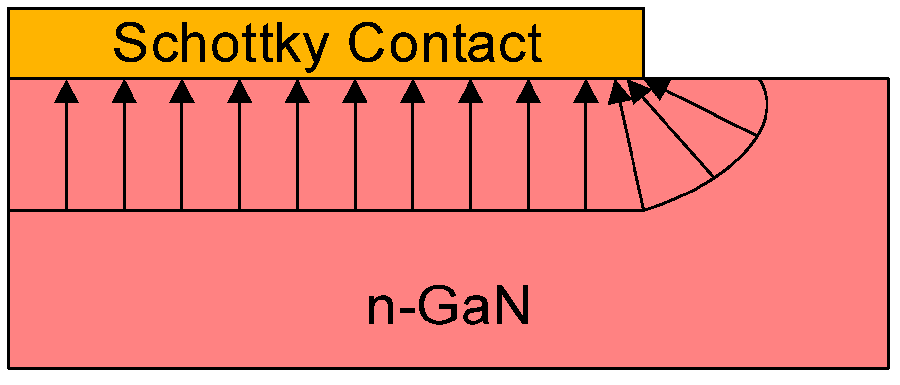
2.2. Reverse Breakdown Characteristics
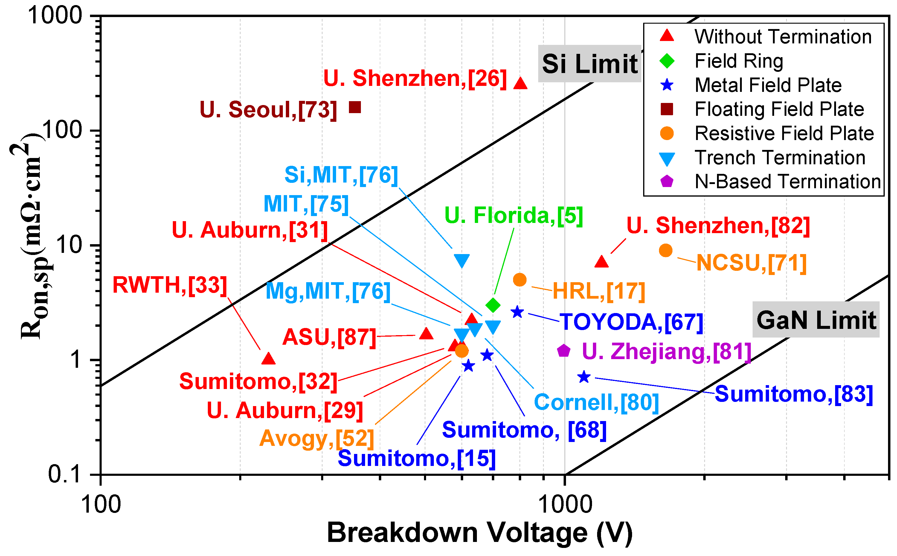
3. Edge Termination Techniques
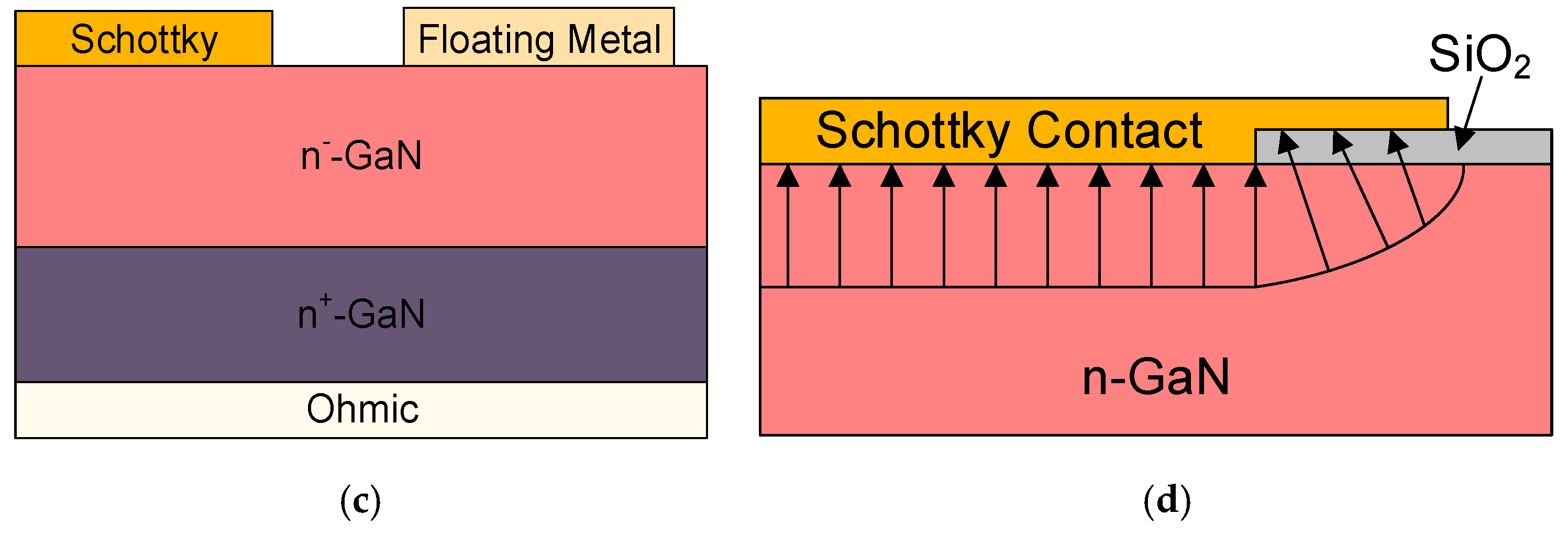
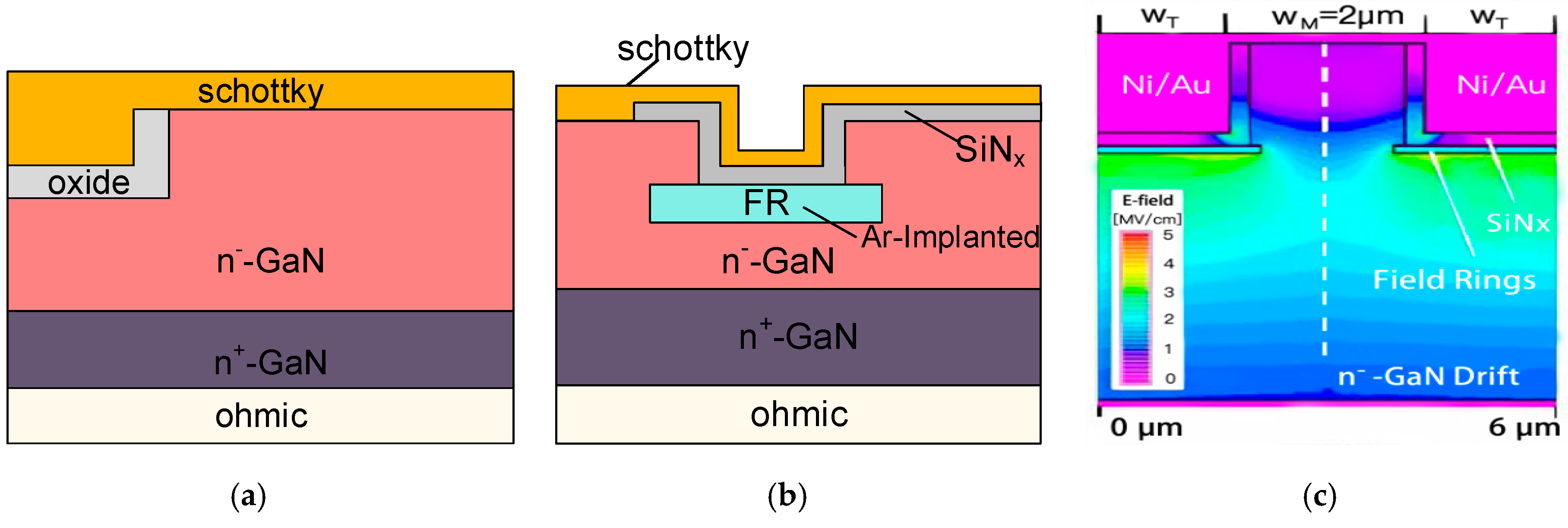
3.1. Field Rings
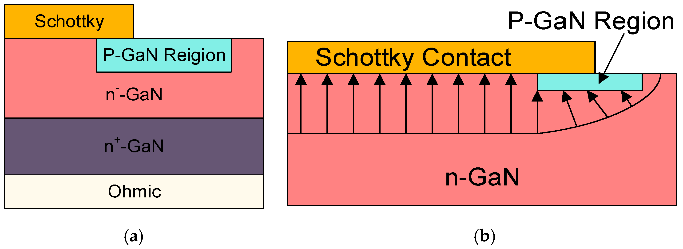
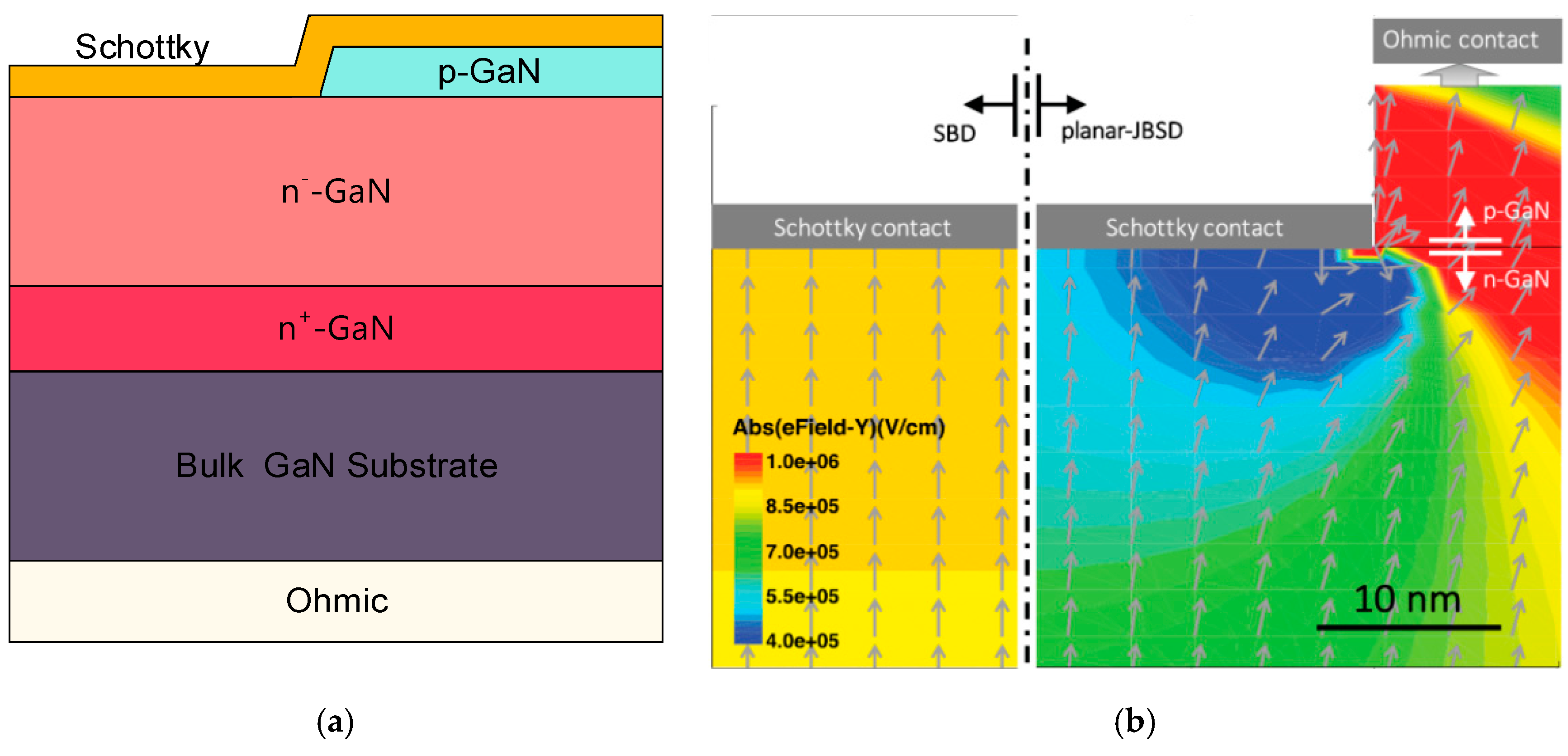
3.2. Junction Termination Extension (JTE)
3.3. Field Plates
3.4. Trench Termiantion
3.5. Reduced Surface Field (RESURF)
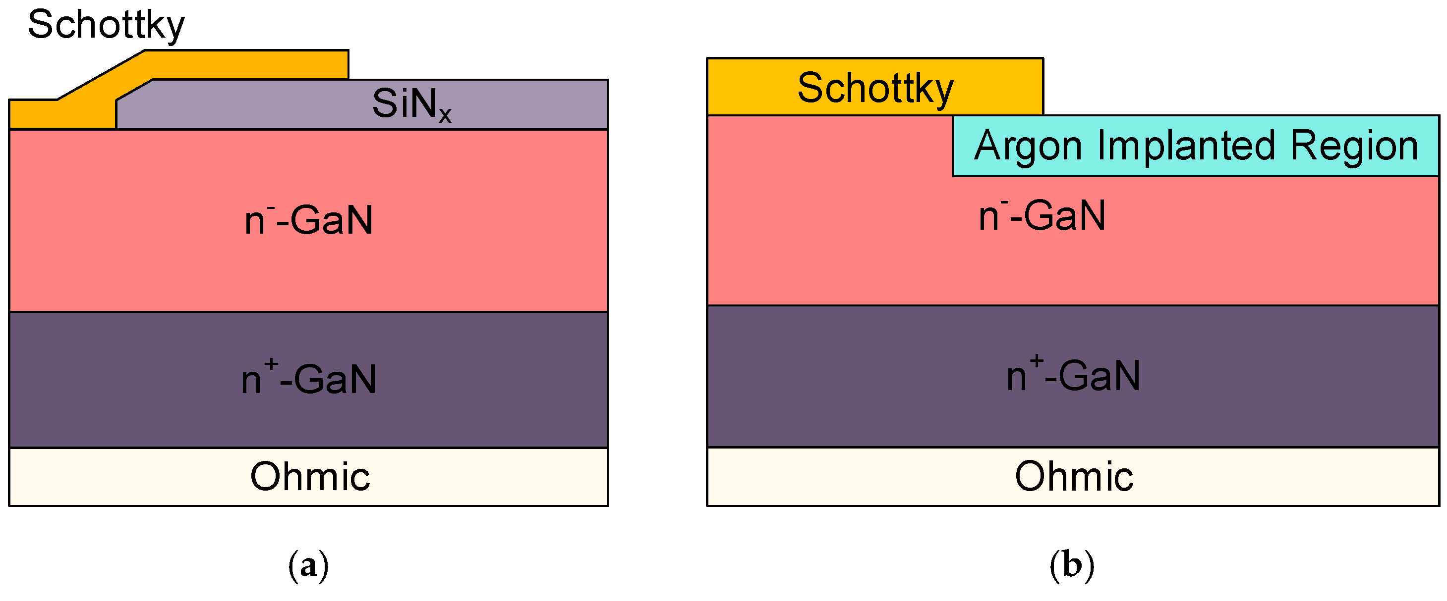
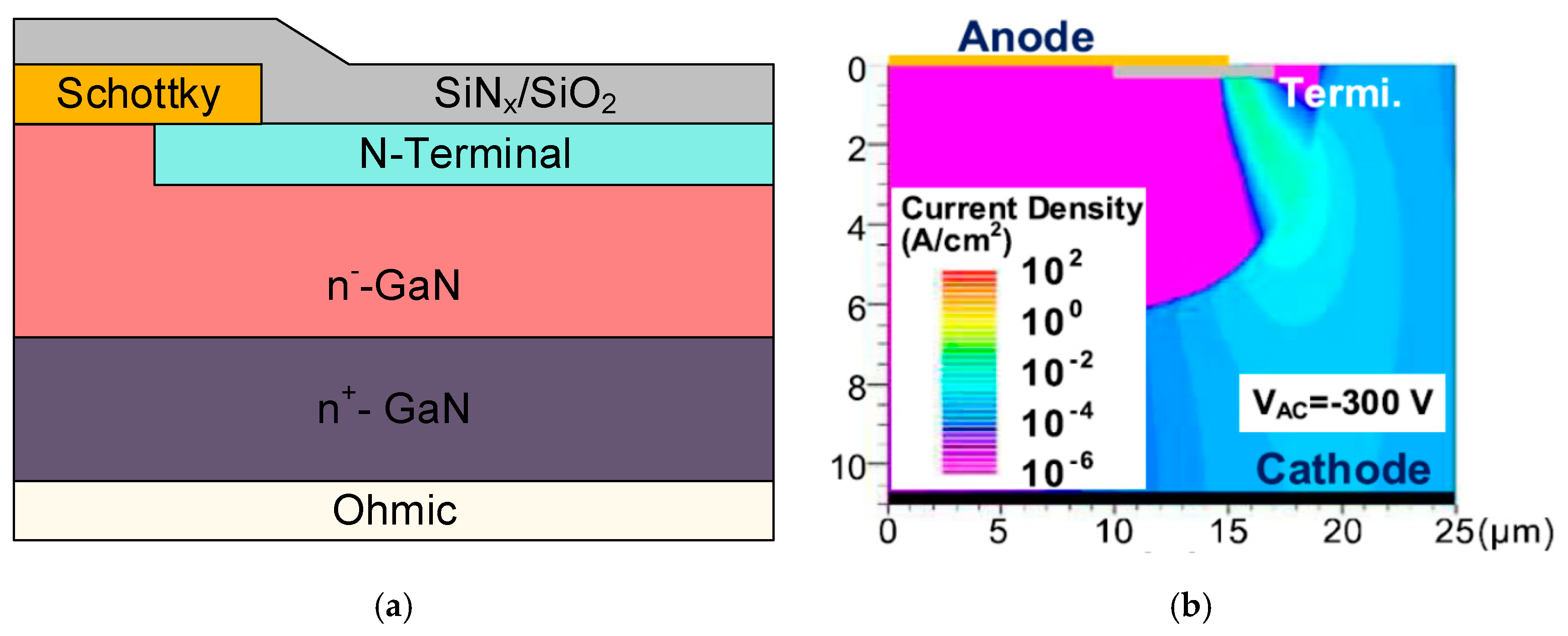
3.6. N-Based Termination
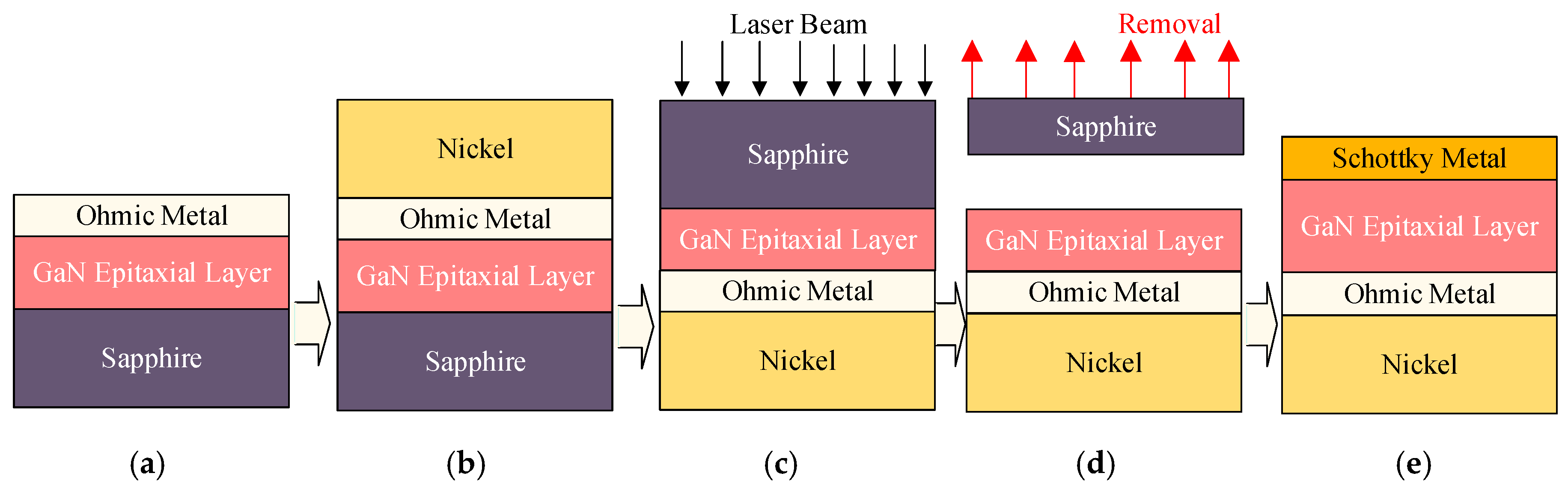
4. Fabrication Steps of Vertical GaN SBDs
5. Conclusions
Author Contributions
Funding
Acknowledgments
Conflicts of Interest
References
- Flack, T.J.; Pushpakaran, B.N.; Bayne, S.B. GaN technology for power electronic applications: A review. J. Electron. Mater. 2016, 45, 2673–2682. [Google Scholar]
- Zhang, Q.G.; Roosmalen, A. More than Moore, 1st ed.; Springer: Berlin/Heidelberg, Germany, 2009; pp. 85–107. [Google Scholar]
- Dang, G.T.; Zhang, A.P.; Mshewa, M.M.; Ren, F.; Chyi, J.I.; Lee, C.M.; Chuo, C.C.; Chi, G.C.; Han, J.; Chu, S.N.G.; et al. High breakdown voltage Au/Pt/GaN Schottky diodes. J. Vac. Sci. Technol. A Vac. Surf. Films 2000, 18, 1135–1138. [Google Scholar] [CrossRef]
- Kang, X.; Wang, X.; Huang, S.; Zhang, J.; Liu, X. Recess-free AlGaN/GaN lateral Schottky barrier controlled Schottky rectifier with low turn-on voltage and high reverse blocking. In Proceedings of the 2018 IEEE 30th International Symposium on Power Semiconductor Devices and ICs (ISPSD), Chicago, IL, USA, 13–17 May 2018. [Google Scholar]
- Zhang, A.P.; JJohnson, W.; Luo, B.; Ren, F.; Pearton, S.J.; Park, S.S.; Park, Y.J.; Chyi, J.I. Vertical and lateral GaN rectifiers on free-standing GaN substrates. Appl. Phys. Lett. 2001, 79, 1555–1557. [Google Scholar] [CrossRef]
- Yang, S.; Han, S.; Li, R.; Sheng, K. 1 kV/1.3 mΩ·cm2 vertical GaN-on-GaN Schottky barrier diodes with high switching performance. In Proceedings of the 2018 IEEE 30th International Symposium on Power Semiconductor Devices and ICs (ISPSD), Chicago, IL, USA, 13–17 May 2018. [Google Scholar]
- Bandić, Z.Z.; Bridger, P.M.; Piquette, E.C.; Mcgill, T.C.; Vaudo, R.P.; Phanse, V.M.; Redwing, J.M. High voltage (450 V) GaN Schottky rectifiers. Appl. Phys. Lett. 1999, 74, 1266–1268. [Google Scholar] [CrossRef]
- Saremi, M. Modeling and Simulation of the Programmable Metallization cells (PMCs) and Diamond-Based Power Devices. Ph.D. Thesis, Arizona State University, Tempe, AZ, USA, 2017. [Google Scholar]
- Jamali Mahabadi, S.E.; Moghadam, H.A. Comprehensive study of a 4H–SiC MES–MOSFET. Phys. E Low-Dimens. Syst. Nanostruct. 2015, 74, 25–29. [Google Scholar] [CrossRef]
- Moghadam, H.A.; Dimitrijev, S.; Han, J.; Haasmann, D.; Aminbeidokhti, A. Transient-Current Method for Measurement of Active Near-Interface Oxide Traps in 4H-SiC MOS Capacitors and MOSFETs. IEEE Trans. Electron Devices 2015, 62, 2670–2674. [Google Scholar] [CrossRef]
- Saremi, M.; Hathwar, R.; Dutta, M.; Koeck, F.A.M.; Nemanich, R.J.; Chowdhury, S.; Goodnick, S.M. Analysis of the reverse I-V characteristics of diamond-based PIN diodes. Appl. Phys. Lett. 2017, 111, 043507. [Google Scholar] [CrossRef]
- Holmes, J.; Dutta, M.; Koeck, F.A.; Benipal, M.; Brown, J.; Fox, B.; Hathwar, R.; Johnson, H.; Malakoutian, M.; Saremi, M.; et al. A 4.5 μm PIN diamond diode for detecting slow neutrons. In Nuclear Instruments and Methods in Physics Research Section A: Accelerators, Spectrometers; Detectors and Associated Equipment; Elsevier: Amsterdam, The Netherlands, 2018; Volume 903, pp. 297–301. [Google Scholar]
- Chante, J.P.; Locatelli, M.L.; Planson, D.; Ottaviani, L.; Morvan, E.; Isoird, K.; Nallet, F. Silicon carbide power devices. In 1998 International Semiconductor Conference; World Scientific Publishing Company: Singapore, 1998. [Google Scholar]
- Baliga, B.J. Gallium nitride devices for power electronic applications. Semicond. Sci. Technol. 2013, 28, 074011. [Google Scholar] [CrossRef]
- Ueno, M.; Yoshimoto, S.; Ishihara, K.; Okada, M.; Sumiyoshi, K.; Hirano, H.; Mitsuhashi, F.; Yoshizumi, Y.; Ishizuka, T.; Kiyama, M.; et al. Fast recovery performance of vertical GaN Schottky barrier diodes on low-dislocation-density GaN substrates. In Proceedings of the 2014 IEEE 26th International Symposium on Power Semiconductor Devices & IC’s (ISPSD), Waikoloa, HI, USA, 15–19 June 2014. [Google Scholar]
- Tanaka, T.; Kaneda, N.; Mishima, T.; Kihara, Y.; Aoki, T.; Shiojima, K. Roles of lightly doped carbon in the drift layers of vertical n-GaN Schottky diode structures on freestanding GaN substrates. Jpn. J. Appl. Phys. 2015, 54, 041002. [Google Scholar] [CrossRef]
- Cao, Y.; Chu, R.; Li, R.; Chen, M.; Chang, R.; Hughes, B. High-voltage vertical GaN Schottky diode enabled by low-carbon metal-organic chemical vapor deposition growth. Appl. Phys. Lett. 2016, 108, 062103. [Google Scholar] [CrossRef]
- Ren, B.; Liao, M.; Sumiya, M.; Wang, L.; Koide, Y.; Sang, L. Nearly ideal vertical GaN Schottky barrier diodes with ultralow turn-on voltage and on-resistance. Appl. Phys. Express 2017, 10, 051001. [Google Scholar] [CrossRef]
- Cao, Y.; Chu, R.; Li, R.; Chen, M.; Williams, A.J. Improved performance in vertical GaN Schottky diode assisted by AlGaN tunneling barrier. Appl. Phys. Lett. 2016, 108, 112101. [Google Scholar] [CrossRef]
- Hu, J.; Zhang, Y.; Sun, M.; Piedra, D.; Chowdhury, N.; Palacios, T. Materials and processing issues in vertical GaN power electronics. Mater. Sci. Semicond. Process. 2018, 78, 75–84. [Google Scholar] [CrossRef]
- Chen, J.; Brewer, W.D. Ohmic Contacts on p-GaN. Adv. Electron. Mater. 2015, 1, 1500113. [Google Scholar] [CrossRef]
- Sundaramoorthy, V.; Nistor, I. Design of quasi-vertical GaN high power Schottky diodes based on field plate termination. In CAS 2010 Proceedings (International Semiconductor Conference); IEEE: Piscataway, NJ, USA, 2010. [Google Scholar]
- Sumiyoshi, K.; Okada, M.; Ueno, M.; Kiyama, M.; Nakamura, T. Low on-resistance high breakdown voltage GaN diodes on low dislocation density GaN substrates. SEI Tech. Rev. 2013, 77, 113. [Google Scholar]
- Motoki, K. Development of gallium nitride substrates. SEI Tech. Rev. 2010, 70, 28–35. [Google Scholar]
- Sang, L.; Ren, B.; Sumiya, M.; Liao, M.; Koide, Y.; Tanaka, A.; Cho, Y.; Harada, Y.; Nabatame, T.; Sekiguchi, T.; et al. Initial leakage current paths in the vertical-type GaN-on-GaN Schottky barrier diodes. Appl. Phys. Lett. 2017, 111, 122102. [Google Scholar] [CrossRef]
- Gu, H.; Hu, C.; Wang, J.; Lu, Y.; Ao, J.-P.; Tian, F.; Zhang, Y.; Wang, M.; Liu, X.; Xu, K.; et al. Vertical GaN Schottky barrier diodes on Ge-doped free-standing GaN substrates. J. Alloy. Compd. 2019, 780, 476–481. [Google Scholar] [CrossRef]
- Kizilyalli, I.C.; Bui-Quang, P.; Disney, D.; Bhatia, H.; Aktas, O. Reliability studies of vertical GaN devices based on bulk GaN substrates. Microelectron. Reliab. 2015, 55, 1654–1661. [Google Scholar] [CrossRef]
- Cao, X.A.; Lu, H.; Leboeuf, S.F.; Cowen, C.; Arthur, S.D.; Wang, W. Growth and characterization of GaN PiN rectifiers on free-standing GaN. Appl. Phys. Lett. 2005, 87, 053503. [Google Scholar] [CrossRef]
- Wang, Y.; Alur, S.; Sharma, Y.; Tong, F.; Thapa, R.; Gartland, P.; Issacs-Smith, T.; Ahyi, C.; Williams, J.; Park, M.; et al. Ultra-low leakage and high breakdown Schottky diodes fabricated on free-standing GaN substrate. Semicond. Sci. Technol. 2010, 26, 022002. [Google Scholar] [CrossRef]
- Baliga, B.J. Fundamentals of Power Semiconductor Devices; Springer: Berlin/Heidelberg, Germany, 2010. [Google Scholar]
- Zhou, Y.; Wang, D.; Ahyi, C.; Tin, C.-C.; Williams, J.; Park, M.; Williams, N.M.; Hanser, A. High breakdown voltage Schottky rectifier fabricated on bulk n-GaN substrate. Solid-State Electron. 2006, 50, 1744–1747. [Google Scholar] [CrossRef]
- Hashimoto, S.; Yoshizumi, Y.; Tanabe, T.; Kiyama, M. High-purity GaN epitaxial layers for power devices on low-dislocation-density GaN substrates. J. Cryst. Growth 2007, 298, 871–874. [Google Scholar] [CrossRef]
- Witte, W.; Fahle, D.; Koch, H.; Heuken, M.; Kalisch, H.; Vescan, A. Electrical properties of quasi-vertical Schottky diodes. Semicond. Sci. Technol. 2012, 27, 085015. [Google Scholar] [CrossRef]
- Johnson, J.W.; Laroch, J.R.; Ren, F.; Gila, B.P.; Overberg, M.E.; Abernathy, C.R.; Chyi, J.I.; Chuo, C.C.; Nee, T.E.; Lee, C.M.; et al. Schottky rectifiers fabricated on free-standing GaN substrates. Solid-State Electron. 2001, 45, 405–410. [Google Scholar] [CrossRef]
- Zhang, K.; Mase, S.; Nakamura, K.; Hamada, T.; Egawa, T. Demonstration of fully vertical GaN-on-Si Schottky diode. Electron. Lett. 2017, 53, 1610–1611. [Google Scholar] [CrossRef]
- Sabui, G.; Zubialevich, V.Z.; White, M.; Pampili, P.; Parbrook, P.J.; Mclaren, M.; Arredondo-Arechavala, M.; Shen, Z.J. GaN Nanowire Schottky Barrier Diodes. IEEE Trans. Electron Devices 2017, 64, 2283–2290. [Google Scholar] [CrossRef]
- Zhang, Y.; Sun, M.; Piedra, D.; Azize, M.; Zhang, X.; Fujishima, T.; Palacios, T. GaN-on-Si vertical Schottky and p-n diodes. IEEE Electron Device Lett. 2014, 35, 618–620. [Google Scholar]
- Liu, C.; Khadar, R.A.; Matioli, E. Vertical GaN-on-Si MOSFETs with monolithically integrated freewheeling Schottky Barrier Diodes. IEEE Electron Device Lett. 2018, 39, 1034–1037. [Google Scholar] [CrossRef]
- Zhang, Y.; Dadgar, A.; Palacios, T. Gallium nitride vertical power devices on foreign substrates: A review and outlook. J. Phys. D Appl. Phys. 2018, 51, 273001. [Google Scholar] [CrossRef]
- Pengelly, R.S.; Wood, S.M.; Milligan, J.W.; Sheppard, S.T.; Pribble, W.L. A review of GaN on SiC high electron-mobility power transistors and MMICs. IEEE Trans. Microw. Theory Tech. 2012, 60, 1764–1783. [Google Scholar] [CrossRef]
- Ma, J.; Zanuz, D.C.; Matioli, E. Field plate design for low leakage current in lateral GaN power Schottky diodes: Role of the pinch-off voltage. IEEE Electron Device Lett. 2017, 38, 1298–1301. [Google Scholar] [CrossRef]
- Baliga, B.J. Power semiconductor device figure of merit for high-frequency applications. IEEE Electron Device Lett. 1989, 10, 455–457. [Google Scholar] [CrossRef]
- Yu, H.; Duan, T. Gallium Nitride Power Devices, 1st ed.; Springer: Berlin/Heidelberg, Germany, 2017; pp. 193–239. [Google Scholar]
- Crowell, C.R.; Sze, S.M. Current transport in metal-semiconductor barriers. Solid-State Electron. 1966, 9, 1035–1048. [Google Scholar] [CrossRef]
- Khemka, V.; Patel, R.; Chow, T.P.; Gutmann, R.J. Design considerations and experimental analysis for silicon carbide power rectifiers. Solid-State Electron. 1999, 43, 1945–1962. [Google Scholar] [CrossRef]
- Baliga, J. Modern Power Devices; John Wiley and Sons Inc.: New York, NY, USA, 1987. [Google Scholar]
- Chow, T.P.; Ramungul, N.; Fedison, J.; Tang, Y. SiC Power Bipolar Transistors and Thyristors, in Silicon Carbide: Recent Major Advances; Choyke, W.J., Matsunami, H., Pensl, G., Eds.; Springer: Berlin/Heidelberg, Germany, 2004; pp. 737–767. [Google Scholar]
- Tsao, J.Y.; Chowdhury, S.; Hollis, M.A.; Jena, D.; Johnson, N.M.; Jones, K.A.; Kaplar, R.J.; Rajan, S.; van de Walle, C.G.; Bellotti, E.; et al. Ultrawide-bandgap semiconductors: Research opportunities and challenges. Adv. Electron. Mater. 2018, 4, 1600501. [Google Scholar] [CrossRef]
- Hasegawa, H.; Oyama, S. Mechanism of anomalous current transport in n-type GaN Schottky contacts. J. Vac. Sci. Technol. B: Microelectron. Nanometer Struct. Process. Meas. Phenom. 2002, 20, 1647–1655. [Google Scholar] [CrossRef]
- Miller, E.J.; Yu, E.T.; Waltereit, P.; Speck, J.S. Analysis of reverse-bias leakage current mechanisms in GaN grown by molecular-beam epitaxy. Appl. Phys. Lett. 2004, 84, 535–537. [Google Scholar] [CrossRef]
- Zhang, H.; Miller, E.J.; Yu, E.T. Analysis of leakage current mechanisms in Schottky contacts to GaN and Al0.25Ga0.75N∕GaN grown by molecular-beam epitaxy. J. Appl. Phys. 2006, 99, 023703. [Google Scholar] [CrossRef]
- Disney, D.; Nie, H.; Edwards, A.; Bour, D.; Shah, H.; Kizilyalli, I.C. Vertical power diodes in bulk GaN. In Proceedings of the 2013 25th International Symposium on Power Semiconductor Devices & IC’s (ISPSD), Kanazawa, Japan, 26–30 May 2013. [Google Scholar]
- Johnson, J.W.; Zhang, A.P.; Wen-Ben, L.; Fan, R.; Pearton, S.J.; Park, S.S.; Park, Y.J.; Jenn-Inn, C. Breakdown voltage and reverse recovery characteristics of free-standing GaN Schottky rectifiers. IEEE Trans. Electron Devices 2002, 49, 32–36. [Google Scholar] [CrossRef]
- Ip, K.; Baik, K.H.; Luo, B.; Ren, F.; Pearton, S.J.; Park, S.S.; Park, Y.J.; Zhang, A.P. High current bulk GaN Schottky rectifiers. Solid-State Electron. 2002, 46, 2169–2172. [Google Scholar] [CrossRef]
- Laroche, J.R.; Ren, F.; Baik, K.W.; Pearton, S.J.; Shelton, B.S.; Peres, B. Design of edge termination for GaN power Schottky diodes. J. Electron. Mater. 2005, 34, 370–374. [Google Scholar] [CrossRef]
- Qi, C.; Wang, Q.; Wang, L.; Liu, Z.; Yi, X.; Li, J.; Wang, J. A novel surface treatment for the sliver ohmic contacts to P-GaN. In Proceedings of the 2016 13th China International Forum on Solid State Lighting (SSLChina), Beijing, China, 15–17 November 2016. [Google Scholar]
- Oh, M.; Kim, H. Highly Reflective Nonalloyed Ni/Ag/Pt Contact to Mg–Si Codoped p-GaN for Enhanced Efficiency of Light-Emitting Diodes. J. Nanosci. Nanotechnol. 2015, 15, 7531–7536. [Google Scholar] [CrossRef]
- Wenzel, R.; Fischer, G.G.; Schmid-Fetzer, R. Ohmic contacts on p-GaN (Part II): Impact of semiconductor fabrication and surface treatment. Mater. Sci. Semicond. Process. 2001, 4, 367–371. [Google Scholar] [CrossRef]
- Feigelson, B.N.; Anderson, T.J.; Abraham, M.; Freitas, J.A.; Hite, J.K.; Eddy, C.R.; Kub, F.J. Multicycle rapid thermal annealing technique and its application for the electrical activation of Mg implanted in GaN. J. Cryst. Growth 2012, 350, 21–26. [Google Scholar] [CrossRef]
- Greenlee, J.D.; Anderson, T.J.; Feigelson, B.N.; Wheeler, V.D.; Hobart, K.D.; Kub, F.J. Comparison of AlN encapsulants for bulk GaN Multicycle rapid thermal annealing. ECS J. Solid State Sci. Technol. 2015, 4, 403–407. [Google Scholar] [CrossRef]
- Koehler, A.D.; Anderson, T.J.; Tadjer, M.J.; Nath, A.; Feigelson, B.N.; Shahin, D.I.; Hobart, K.D.; Kub, F.J. Vertical GaN junction barrier Schottky diodes. ECS J. Solid State Sci. Technol. 2016, 6, 10–12. [Google Scholar] [CrossRef]
- Anderson, T.J.; Feigelson, B.N.; Kub, F.J.; Tadjer, M.J.; Hobart, K.D.; Mastro, M.A.; Hite, J.K.; Eddy, C.R., Jr. Activation of Mg implanted in GaN by multicycle rapid thermal annealing. Electron. Lett. 2014, 50, 197–198. [Google Scholar] [CrossRef]
- Greenlee, J.D.; Feigelson, B.N.; Anderson, T.J.; Hite, J.K.; Hobart, K.D.; Kub, F.J. Symmetric multicycle rapid thermal annealing: Enhanced activation of implanted dopants in GaN. ECS J. Solid State Sci. Technol. 2015, 4, 382–386. [Google Scholar] [CrossRef]
- Temple, V.A.K. Junction termination extension (JTE), A new technique for increasing avalanche breakdown voltage and controlling surface electric fields in P-N junctions. In Proceedings of the 1977 International Electron Devices Meeting, Washington, DC, USA, 5–7 December 1977. [Google Scholar]
- Anderson, T.J.; Greenlee, J.D.; Feigelson, B.N.; Hite, J.K.; Kub, F.J.; Hobart, K.D. Improved vertical GaN Schottky diodes with ion implanted junction termination extension. ECS J. Solid State Sci. Technol. 2016, 5, 176–178. [Google Scholar] [CrossRef]
- Baliga, B.J. Advanced Power Rectifier Concepts; Springer: Berlin/Heidelberg, Germany, 2009. [Google Scholar]
- Tanaka, N.; Hasegawa, K.; Yasunishi, K.; Murakami, N.; Oka, T. 50 A vertical GaN Schottky barrier diode on a free-standing GaN substrate with blocking voltage of 790 V. Appl. Phys. Express 2015, 8, 071001. [Google Scholar] [CrossRef]
- Horii, T.; Miyazaki, T.; Saito, Y.; Hashimoto, S.; Tanabe, T.; Kiyama, M. High-breakdown-voltage GaN vertical Schottky barrier diodes with field plate structure. Mater. Sci. Forum 2009, 15, 963–966. [Google Scholar] [CrossRef]
- Zhang, Y.; Sun, M.; Wong, H.; Lin, Y.; Srivastava, P.; Hatem, C.; Azize, M.; Piedra, D.; Yu, L.; Sumitomo, T.; et al. Origin and control of off-state leakage current in GaN-on-Si vertical diodes. IEEE Trans. Electron. Devices 2015, 62, 2155–2161. [Google Scholar] [CrossRef]
- Ozbek, A.M.; Baliga, B.J. Finite-Zone Argon implant edge termination for high-voltage GaN Schottky rectifiers. IEEE Electron Device Lett. 2011, 32, 1361–1363. [Google Scholar] [CrossRef]
- Ozbek, A.M.; Baliga, B.J. Planar nearly ideal edge-termination technique for GaN devices. IEEE Electron Device Lett. 2011, 32, 300–302. [Google Scholar] [CrossRef]
- Grove, A.S.; Leistiko, O.; Hooper, W.W. Effect of surface fields on the breakdown voltage of planar silicon p-n junctions. IEEE Trans. Electron Devices 1967, 14, 157–162. [Google Scholar] [CrossRef]
- Seung-Chul, L.; Jin-Cherl, H.; Soo-Seong, K.; Min-Woo, H.; Kwang-Seok, S.; Yearn-Ik, C.; Min-Koo, H. A new vertical GaN Schottky barrier diode with floating metal ring for high breakdown voltage. In Proceedings of the 2004 Proceedings of the 16th International Symposium on Power Semiconductor Devices and ICs, Kitakyushu, Japan, 24–27 May 2004. [Google Scholar]
- Bhatnagar, M.; Nakanishi, H.; Bothra, S.; Mclarty, P.K.; Baliga, B.J. Edge terminations for SiC high voltage Schottky rectifiers. In Proceedings of the 5th International Symposium on Power Semiconductor Devices and ICs, Monterey, CA, USA, 18–20 May 1993. [Google Scholar]
- Zhang, Y.; Sun, M.; Liu, Z.; Piedra, D.; Pan, M.; Gao, X.; Lin, Y.; Zubair, A.; Yu, L.; Palacios, T.; et al. Novel GaN trench MIS barrier Schottky rectifiers with implanted field rings. In Proceedings of the 2016 IEEE International Electron Devices Meeting (IEDM), San Francisco, CA, USA, 3–7 December 2016. [Google Scholar]
- Zhang, Y.; Liu, Z.; Tadjer, M.J.; Sun, M.; Piedra, D.; Hatem, C.; Anderson, T.J.; Luna, L.E.; Nath, A.; Palacios, T.; et al. Vertical GaN junction barrier Schottky rectifiers by selective ion implantation. IEEE Electron Device Lett. 2017, 38, 1097–1100. [Google Scholar] [CrossRef]
- Qiao, M.; Hu, X.; Wen, H.; Wang, M.; Luo, B.; Luo, X.; Wang, Z.; Zhang, B.; Li, Z. A novel substrate-assisted RESURF technology for small curvature radius junction. In Proceedings of the 2011 IEEE 23rd International Symposium on Power Semiconductor Devices and ICs, San Diego, CA, USA, 23–26 May 2011. [Google Scholar]
- Ludikhuize, A.W. A review of RESURF technology. In Proceedings of the 12th International Symposium on Power Semiconductor Devices and ICs, Toulouse, France, 22–25 May 2000. [Google Scholar]
- Qiao, M.; Wang, Y.; Zhou, X.; Jin, F.; Wang, H.; Wang, Z.; Li, Z.; Zhang, B. Analytical modeling for a novel triple RESURF LDMOS with N-Top layer. IEEE Trans. Electron Devices 2015, 62, 2933–2939. [Google Scholar] [CrossRef]
- Li, W.; Nomoto, K.; Pilla, M.; Pan, M.; Gao, X.; Jena, D.; Xing, H.G. Design and realization of GaN trench junction-barrier-Schottky-diodes. IEEE Trans. Electron Devices 2017, 64, 1635–1641. [Google Scholar] [CrossRef]
- Han, S.; Yang, S.; Sheng, K. High-voltage and high-Ion/Ioff vertical GaN-on-GaN Schottky barrier diode with nitridation-based termination. IEEE Electron Device Lett. 2018, 39, 572–575. [Google Scholar] [CrossRef]
- Liu, X.; Liu, Q.; Li, C.; Wang, J.; Yu, W.; Xu, K.; Ao, J.-P. 1.2 kV GaN Schottky barrier diodes on free-standing GaN wafer using a CMOS-compatible contact material. Jpn. J. Appl. Phys. 2017, 56, 026501. [Google Scholar] [CrossRef]
- Saitoh, Y.; Sumiyoshi, K.; Okada, M.; Horii, T.; Miyazaki, T.; Shiomi, H.; Ueno, M.; Katayama, K.; Kiyama, M.; Nakamura, T.; et al. Extremely low on-resistance and high breakdown voltage observed in vertical GaN Schottky barrier diodes with high-mobility drift layers on low-dislocation-density gan substrates. Appl. Phys. Express 2010, 3, 081001. [Google Scholar] [CrossRef]
- Shui-Jinn, W.; Shu-Cheng, C.; Uang, K.; Bor-Wen, L. Vertical-structured Ni/n-GaN schottky diode with electroplating nickel substrate. In Proceedings of the 63rd Device Research Conference Digest, Santa Barbara, CA, USA, 20–22 June 2005. [Google Scholar]
- Mastro, M.; Kryliouk, O.; Reed, M.; Anderson, T.; Davydov, A.; Shapiro, A. Thermal stability of MOCVD and HVPE GaN layers in H2, HCl, NH3 and N2. Phys. Status Solidi A 2001, 188, 467–471. [Google Scholar] [CrossRef]
- Zhu, T.G.; Lambert, D.J.H.; Shelton, B.S.; Wong, M.M.; Chowdhury, U.; Dupuis, R.D. High-voltage mesa-structure GaN Schottky rectifiers processed by dry and wet etching. Appl. Phys. Lett. 2000, 77, 2918–2920. [Google Scholar] [CrossRef]
- Fu, H.; Huang, X.; Chen, H.; Lu, Z.; Baranowski, I.; Zhao, Y. Ultra-low turn-on voltage and on-resistance vertical GaN-on-GaN Schottky power diodes with high mobility double drift layers. Appl. Phys. Lett. 2017, 111, 152102. [Google Scholar] [CrossRef]
- Zhang, A.P.; Dang, G.; Ren, F.; Han, J.; Cho, H.; Pearton, S.J.; Chyi, J.I.; Nee, T.E.; Lee, C.M.; Chu, S.N.G.; et al. Forward turn-on and reverse blocking characteristics of GaN Schottky and p-i-n rectifiers. Solid-State Electron. 2000, 44, 1157–1161. [Google Scholar] [CrossRef]


| Materials | Eg (eV) | ε | μn (cm2/V·s) | Ec (MV/cm) | Vsat (107cm/s) | Total Dislocation (cm2) | Thermal Conductivity (W/m·K) |
|---|---|---|---|---|---|---|---|
| Si | 1.12 | 11.8 | 1350 | 0.3 | 1 | - | 145 |
| GaAs | 1.42 | 13.1 | 8500 | 0.4 | 2 | - | 50 |
| 4H-SiC | 3.26 | 10 | 720 | 2.0 | 2 | >102 | 370 |
| GaN | 3.44 | 9 | 1250 | 3.3 | 2.5 | >105 | 253 |
| Diamond | 5.5 | 5.7 | 2000 | 13.0 | 1.5 | >104 | 2290 |
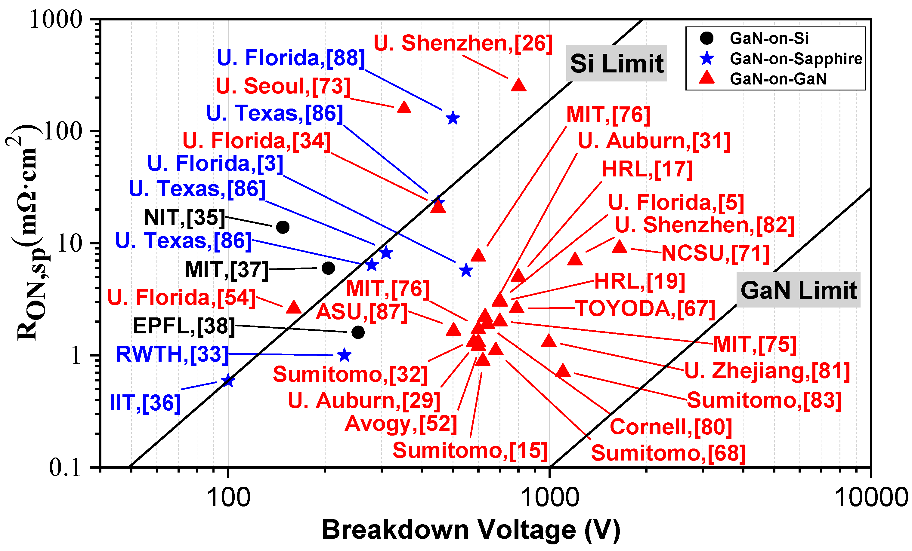
| Year | Substrate | BV (V) | RON,sp (mΩ·cm2) | VON (V) | Schottky Metal | Ohmic Metal | Manufacturer | Ref. |
|---|---|---|---|---|---|---|---|---|
| 1999 | Sapphire | 450 | NA | 4.2 | Au | Ti/Al/Ni/Au | CIT | [7] |
| 2000 | Sapphire | 550 | 5.7 | 3.5 | NA | Pt/Au | U. Florida | [3] |
| 2000 | Sapphire | 450 | 23 | N.A | Pt/Au | Ti/Al/Pt/Au | U. Texas | [86] |
| 2000 | Sapphire | 310 | 8.2 | N.A | Pt/Au | Ti/Al/Pt/Au | U. Texas | [86] |
| 2000 | Sapphire | 280 | 6.4 | N.A | Pt/Au | Ti/Al/Pt/Au | U. Texas | [86] |
| 2000 | Sapphire | 500 | 130 | 3.5 | Ni/Pt/Au | Ti/Al/Pt/Au | U. Florida | [88] |
| 2001 | GaN | 450 | 20.5 | 3 | Pt/Au | Ti/Al | U. Florida | [34] |
| 2001 | GaN | 700 | 3.01 | 1.8 | Pt/Ti/Au | Ti/Al/Pt/Au | U. Florida | [5] |
| 2002 | GaN | 160 | 2.6 | 1.8 | Pt/Ti/Au | Ti/Al/Pt/Au | U. Florida | [54] |
| 2002 | GaN | 160 | 3 | 1.8 | Pt/Ti/Au | Ti/Al/Pt/Au | U. Florida | [53] |
| 2004 | GaN | 353 | 160 | NA | Pd/Mo/Ti/Au | Ti/Al/Ni/Au | Seoul | [73] |
| 2006 | GaN | 630 | 2.2 | 1.2 | Pt | Ti/Al | U. Auburn | [31] |
| 2007 | GaN | 580 | 1.3 | 1.35 | Au | Ti/Al/Ti/Au | Sumitomo | [32] |
| 2009 | GaN | 680 | 1.1 | 1.2 | Au | Ti/Al/Ti/Au | Sumitomo | [68] |
| 2010 | GaN | 1100 | 0.71 | 1 | Ni/Au | Ti/Al/Ti/Au | Sumitomo | [83] |
| 2010 | GaN | 600 | 1.3 | 0.95 | Pt | Ti/Al/Ni/Au | U. Auburn | [29] |
| 2011 | GaN | 1650 | 9 | 0.5 | Pt | Ti/Al/Ni/Au | NCSU | [71] |
| 2011 | Sapphire | 1700 | NA | NA | Ni | NA | NCSU | [70] |
| 2012 | Sapphire | 230 | 1 | NA | Ni/Au | Ti/Al/Ni/Au | RWTH | [33] |
| 2013 | GaN | 600 | 1.2 | 0.9 | Pd | Al | Avogy | [52] |
| 2014 | Si | 205 | 6 | 0.5 | Ni/Au | Ti/Al | MIT | [37] |
| 2014 | GaN | 620 | 0.89 | 1.46 | Ni/Au | NA | Sumitomo | [15] |
| 2015 | GaN | 790 | 2.25~2.61 | 0.5 | Ni | Ti/Al | TOYODA | [67] |
| 2016 | GaN | 300 | NA | NA | Ni/Au | Ti/Al/Ni/Au | Naval | [65] |
| 2016 | GaN | 800 | 4.94 | 0.77 | Ni/Au | Ti/Au | HRL | [17] |
| 2016 | GaN | 700 | 3.06 | 0.67 | Ni/Au | Ti/Au | HRL | [19] |
| 2016 | GaN | 700 | 2 | 0.8 | Ni/Au/Ni | Ti/Al | MIT | [75] |
| 2017 | GaN | NA | 0.72 | 0.73 | Ni/Au | Ti/Al/Au | MANA | [18] |
| 2017 | GaN | 610 | NA | 0.5 | Pd/Au | Ti/Al/Ni/Au | Naval | [61] |
| 2017 | GaN | 503 | 1.65 | 0.59 | Pt/Au | Tt/Al/Ti/Au | ASU | [87] |
| 2017 | GaN | 1200 | 7 | 0.69 | TiN | Ti/Al | U. Shenzhen | [82] |
| 2017 | GaN | 600 | 1.7 | 3.5 | Ni/Au | Ti/Al | MIT | [76] |
| 2017 | GaN | 600 | 7.6 | 0.7 | Ni/Au | Ti/Al | MIT | [76] |
| 2017 | Sapphire | 100 | 0.59 | 0.75 | Ni/Ti/Pt/Au | NA | IIT | [36] |
| 2017 | Si | 148 | 13.9 | 0.69 | Ni/Au | AuSb/Au | NIT | [35] |
| 2017 | GaN | 640 | 1.9 | 1 | Pd | Ti/Au | Cornell | [80] |
| 2018 | GaN | 995 | 1.3 | 1.7 | Pt/Au | Ti/Al/Au | U. Zhejiang | [81] |
| 2018 | Si | 254 | 1.6 | 0.76 | Ni/Au | NA | EPFL | [38] |
| 2019 | GaN | 802 | 250 | 0.74 | Ni/Au | Ti/Al/Ni/Au | U. Shenzhen | [26] |
© 2019 by the authors. Licensee MDPI, Basel, Switzerland. This article is an open access article distributed under the terms and conditions of the Creative Commons Attribution (CC BY) license (http://creativecommons.org/licenses/by/4.0/).
Share and Cite
Sun, Y.; Kang, X.; Zheng, Y.; Lu, J.; Tian, X.; Wei, K.; Wu, H.; Wang, W.; Liu, X.; Zhang, G. Review of the Recent Progress on GaN-Based Vertical Power Schottky Barrier Diodes (SBDs). Electronics 2019, 8, 575. https://doi.org/10.3390/electronics8050575
Sun Y, Kang X, Zheng Y, Lu J, Tian X, Wei K, Wu H, Wang W, Liu X, Zhang G. Review of the Recent Progress on GaN-Based Vertical Power Schottky Barrier Diodes (SBDs). Electronics. 2019; 8(5):575. https://doi.org/10.3390/electronics8050575
Chicago/Turabian StyleSun, Yue, Xuanwu Kang, Yingkui Zheng, Jiang Lu, Xiaoli Tian, Ke Wei, Hao Wu, Wenbo Wang, Xinyu Liu, and Guoqi Zhang. 2019. "Review of the Recent Progress on GaN-Based Vertical Power Schottky Barrier Diodes (SBDs)" Electronics 8, no. 5: 575. https://doi.org/10.3390/electronics8050575
APA StyleSun, Y., Kang, X., Zheng, Y., Lu, J., Tian, X., Wei, K., Wu, H., Wang, W., Liu, X., & Zhang, G. (2019). Review of the Recent Progress on GaN-Based Vertical Power Schottky Barrier Diodes (SBDs). Electronics, 8(5), 575. https://doi.org/10.3390/electronics8050575